Optical waveguides with a propagation loss of around 0.5 dB/cm are written inside photosensitive Foturan glass by internal modification of refractive index using ...
3D integration of microfluidics and microoptics inside photosensitive glass by femtosecond laser direct writing for photonic biosensing Koji Sugioka, Zhongke Wang, Katsumi Midorikawa RIKEN – The Institute of Physical and Chemical Research, Wako, Saitama 351-0198, Japan ABSTRACT Optical waveguides with a propagation loss of around 0.5 dB/cm are written inside photosensitive Foturan glass by internal modification of refractive index using femtosecond (fs) laser. Integration of the optical wafveguides with a micromirror enables us to bend the guided laser beam at an angle of 90° with a bending loss of less than 0.3 dB. In the meanwhile, a plano-convex microlens is completely embedded inside the Foturan glass chip via formation of a threedimensional (3D) hollow microstructure using fs laser direct writing followed by heat treatment and successive wet etching. This technique can also be used to fabricate microfluidic devices and therefore realizes 3D integration of microoptical and microfluidic components by one continuous procedure. Subsequently, microoptical waveguides are further integrated into the single glass chip. Demonstration of optical measurements using the integrated microchip reveals that photonic biosensing can be performed with an efficiency increased by a factor of 8 for fluorescence detection and by a factor of 3 for absorption detection. Keywords: femtosecond laser direct writing, biophotonic microchip, optical waveguide, microlens, microfluidics, 3D integration
1. INTRODUCTION In the “lab-on-a-chip” or micro-total analysis system (µ-TAS) devices, a light beam is often required to illuminate a liquid sample in a microfluidic chamber to accomplish photonic biosensing, such as photoabsorption or fluorescence detection.1 Optical waveguides are a highly efficient way to guide the light, and can be connected to an optical spectrometer or photodetector to collect the light transmitted by or emitted from the liquid sample. Therefore, some groups are attempting to integrate the optical waveguides with microfluidic components in a single chip.2 Further integration of microoptical components such as a microlens is expected to enhance the efficiencies of inducing and/or collecting signals in optical analysis. For this purpose, micromirrors were fabricated inside Foturan glass.3 Furthermore, the fabrication of cylindrical and hemispherical microlenses made of Foturan glass by femtosecond (fs) laser processing has been reported.4 In these cases, however, the microlenses were gouged out from the bulk. In this study, we demonstrate the waveguide writing inside photosensitive Foturan glass by internal modification of refractive index using fs laser. We also fabricate a plano-convex microlens that is completely buried inside bulk Foturan glass by the fs laser direct wring followed by thermal treatment and successive chemical wet etching. Then, we attempt to three-dimensionally (3D) integrate the microlens with the optical waveguide and a microfluidic chamber in a single glass chip. Finally, the analyses of fluorescence and absorption from liquid samples are demonstrated by using the 3D integrated microchip.
2. EXPERIMENTAL Experiments were carried out by a commercial fs laser workstation.5 The laser wavelength, pulse width and repetition rate were 775 nm, 150 fs and 1 kHz, respectively. The focusing system was a 20 x microscope objective with a numerical aperture (N.A.) of 0.46. The substrate used in this study for 3D microstructuring is photosensitive glass that is commercially available under the trade name of Foturan from Schott Glass Corporation6. Samples under fabrication were translated by a PC controlled xyz stage for 3D microstructuring. For fabrication of the 3D hollow microstructures such as micromirrors, microlenses and microfluidic components, the typical irradiation condition of fs laser was a fluence of 78 mJ/cm2 and a scanning speed of 510 mm/s. After the fs laser exposure step, the sample was subjected to a programmed annealing, and then soaked in a 10% HF solution with an ultrasonic bath at variable period of etching time, depending on the size of the hollow structures. The laser-exposed regions can be preferentially etched away with a contrast ratio of ca. Photon Processing in Microelectronics and Photonics VII, edited by Andrew S. Holmes, Michel Meunier, Craig B. Arnold, Hiroyuki Niino, David B. Geohegan, Frank Träger, Jan J. Dubowski, Proc. of SPIE Vol. 6879, 68790M, (2008) · 0277-786X/08/$18 · doi: 10.1117/12.762531 Proc. of SPIE Vol. 6879 68790M-1 2008 SPIE Digital Library -- Subscriber Archive Copy
����� �"��� "%$ ���! �
���
� �% �#� )��� ��� (��� �� � �% �#� )��� �� ��(��� �� �� � �% �#� )��� �� �(��� �� ��
��
�� Laser: 1.0 µJ
�
Fig. 1. Near field pattern of He-Ne laser beam guided by the 10mm long optical waveguide written by the fs laser direct writing. Pulse energy and scanning speed were 0.5 µJ and 200 µm/s, respectively.
50 in etching selectivity. Lastly we baked the photosensitive glass sample again to smooth the etched surfaces. The details of procedures and mechanism of selective etching of photosensitive glass are described elsewhere.5, 7, 8 In the meanwhile, for the optical waveguide writing, the tightly focused fs laser beam was scanned inside the samples by moving the samples perpendicularly to the laser beam axis using a PC-controlled xyz stage without the annealing and the successive wet etching.9 The typical writing condition is 0.5 µJ/pulse of laser power and 200 µm/s of scanning speed.
����� �"��� "%$ ���! �
���
��
�
��
��
��
� �%��!�$��"��'�&��%������ �#� )��� � �(��� �� �� �% �#� )��� � ���(��� ��� � � �% �#� )��� ���� (��� ����
��
�� Laser: 2.0 µJ
�
��
�
��
��
��
��!�$��"��'�&��%������ Fig. 2. Optical loss in dependence on the length for waveguides written at different laser energy and scanning speed. Linear fit equations give propagation loss in dB/cm (slope) and coupling loss in dB (y-intercept), same thereafter.
3. OPTICAL WAVEGUIDE WRITING The optical waveguide can be embedded inside the photosensitive glass by fs laser direct writing without post annealing and successive wet etching due to refractive index increase of the laser exposed regions. However, the written waveguides showed a strongly elliptical cross section extending 20-80 µm along the z direction, that is, laser beam propagation direction and only 4-7 µm in the y direction. In order to improve the cross sectional shape, the slit method is very simple and convenient but powerful.10 When a slit of 0.2 mm width was inserted above the objective lens, the elliptical cross sectional shape was significantly improved to an almost circular shape. Different ellipticities can be achieved by adjusting the width of the slit used. Figure 1 shows an example of near field pattern of He-Ne laser beam guided by the written optical waveguide, showing a single-mode pattern. The propagation loss at 632.8 nm was evaluated by fabricating three waveguides of different lengths under the same condition in coupons separated from an identical substrate. Due care was taken to assure that identical coupling conditions are achieved for all three waveguides. The several measurements were taken for each waveguide and the average was adopted. The throughout data for optical loss as a function of waveguide length is shown in Fig. 2. Equations with linear fitting parameters are inserted for different laser writing parameters. The slope of the linear fit represents the propagation loss in dB/cm and the y-intercept gives the coupling loss from both facets of each waveguide. It is clear that the coupling loss is induced by either the unmatched size or the misalignment between the waveguide and the focused He–Ne laser beam. However, the values obtained under the different conditions shown here are quite similar and range of 1.5 to 1.6 dB. The propagation loss is around 0.5 dB/cm for all samples under the conditions investigated.
Proc. of SPIE Vol. 6879 68790M-2
ide (I, II) I, Pin
����� �"��� "$#�� �!�
Micromirror made of embedded hollow plate
��� Pout
� (��� � � �'��� ��� �
�� Mirror
Pin
�
��
�
��
��
�
��
��!�#��"��&�%��$���������
Fig. 3. The schematic illustration of the fabricated structures used to characterize the bending loss of waveguide.
Fig. 4. Optical loss of the waveguides integrated to mirrors, written with 1.0 µJ in pulse energy at scan speed of 200 µm/s.
4. INTEGRATION OF OPTICAL WAVEGUIDE WITH MICROMIRROR From the point of practical view, a light beam guided by the waveguide is often needed to be bent when used to integrate into optical microcomponents and microfluidics. For bending the beam, the curved waveguide is commonly fabricated. In this case the bending loss is an important issue that we cannot be disregard. To minimize the bending loss, the curvature of the curved waveguide should be larger than multiple millimeters, i.e., 5–6 mm, but this causes undesirable increase of device size. In the meanwhile, integration of two straight waveguides with a mirror would significantly shrink the device size.11 We can fabricate a micromirror made of a hollow plate inside Foturan glass by fs laser direct writing followed by thermal treatment and successive wet etching3 and thereby can integrate the waveguides to the micromirror. Figure 3 shows the schematic illustration of the fabricated structures. We fabricated three different structures in which one waveguide (waveguide I) of a constant length is connected to the micromirror of a hollow structure with an angle of 45° and further connected to another waveguide (waveguide II) of different lengths at an angle of 90°. Figure 4 shows the total optical loss for the integrated waveguide with different lengths. The propagation loss is evaluated to be 0.48 dB/cm, which almost corresponds to that of straight waveguides, as shown in Fig. 2. The y-intercept gives the loss including the coupling loss and bending loss at the mirror. Assuming the coupling loss to be the same as that of a single straight fiber (approx. 1.5 dB), one can estimate the bending loss to be less than 0.3 dB. The bending loss may be composed of the reflection loss at the mirror and the coupling loss to the second waveguide. Two parallel mirrors integrated with three waveguides were also fabricated to form a hook-shaped structure. The evaluated bending loss increased slightly in this case because of the increase in the number of bending points.
5. FABRICATION OF EMBEDDED MICROLENS Microlens fabrication was carried out by the technique fabricating the hollow microstructure inside the Foturan glass.12 The fabricated hollow structures always have openings at either the top or bottom or both in a Foturan glass chip, and one of the internal sidewalls of the hollow structure has a spherical shape, i.e., a plano-concave hollow structure, as shown in Fig. 5. The curvature of the spherical shape exactly corresponds to the designed optical microlens curvature; accordingly, this curved surface could work as a plano-convex lens, thus, a microoptical lens could be fabricated inside a glass chip. We first edited the laser writing programs for microlens fabrication. We calculated the required numbers of laser scanning lines in accordance with the given microlens curvature radius R. Then laser scanning was performed line by line at a pitch of 5 µm in a plane at a scanning speed of 2 mm/s and pulse energy of 2.1 µJ. After completing the scan of one plane, the laser beam was shifted layer by layer along the z-direction shown in Fig. 5 with a step of 10 µm from the
Proc. of SPIE Vol. 6879 68790M-3
Hollow Structure
Z
Plano -convex microlens
Plano-concave hollow Plano-convex microlens
y X Glass chip
Schematic illustration of microlens
Top view of microlens inside a glass chip
2Ojtm b) Magnification
100 p.m
Surface morphology
Fig. 5. Schematic illustration and optical microscope images of microlens buried in glass.
Fig. 6. CCD camera images of He-Ne laser beam transmitted by the glass microchip: a) without microlens; b) with microlens.
bottom to the top. After fs laser direct writing to form a 3D latent image of the microlens inside the glass, the thermal treatment, wet chemical etching and additional thermal treatment were employed. Finally, a plano-concave hollow structure is formed in the glass. Thus, the microlens was fabricated inside the glass. Figure 5 also presents the optical microscope images of the plano-convex microlens fabricated inside a glass chip with a thickness of 2 mm, whose curvature radius R and focal length are 0.75 mm (designed value) and 1.5 mm (calculated from the formula: 1/f = (n-1)·(1/R), n = 1.5 (refractive index of Foturan glass)) , respectively. It shows that one of the sidewalls of the buried hollow structure has a spherical shape with a smooth surface, although a small bump can be seen on the lens surface. The average roughness of the etched and then post-annealed surface was evaluated to be 0.8 nm in the area of 20 � 20 µm2 that is good enough for optical applications.3 In order to examine the focusing performance of the microlens, we simply irradiated a He-Ne laser such that it passed through the microlens inside the glass, and the focused laser beam was projected onto a CCD camera using a 20� objective lens with a numerical aperture (N.A.) of 0.35. When a He-Ne laser beam passed through the microlens inside the glass, clearly, the light beam was focused to a tiny spot by the plano-convex microlens, as exhibited in Fig. 6. The focal spot size was measured to be approximately 30 µm in diameter for an incident He-Ne laser beam of �1.5 ~ 1.8 mm. Furthermore, we roughly estimated the focal length experimentally by optical microscope observation, i.e., when a He-Ne beam was passing through the glass chip, simply, a image of the complete chip with a focused beam spot was taken using optical microscopy. The measured focal length was around 1.7 mm, which is slightly longer than the designed value of 1.5 mm. Reflection at an air-glass interface should be responsible for the longer length, i.e., the laser beam is reflected by the flat internal wall of the hollow structure after the lens. Somewhat imperfect fabrication precision could be another reason. However, the focusing results still indicate that the smooth spherical surface of the buried hollow structure is sufficient for optical application. The experimental value of the focal spot size is much larger than the theoretical value of 0.91 µm if calculated using the formula: �0 = 1.27 (�f/D)M2, here, f means the focal length (1.7 mm) of the microlens, � and D represent the wavelength (632.8 nm) and beam diameter (1.5 mm) of the He-Ne laser, respectively. M2 corresponds to
Proc. of SPIE Vol. 6879 68790M-4
Hollow structure I
Plano -convex microlens II Microfluidic chamber Waveguide
Plano -convex microlens I Pump laser, Nd:YAG 532 nm, 15 Hz
�����������������������
Fluorescence detector
Hollow structure II
�����������������������
Absorption detector
����
With microlens
��� ��� ���� ���� � ���� ��
��
���
���
��
��
��
��
���
Without microlens ��������������
���� ���� ��� �
��
��
���
���
��
��
��
��
���
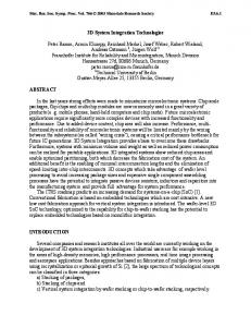
�������������� Fig. 7. Schematic configuration of 3D integration of a microoptical plano-convex lens with a microchamber and an optical waveguide in a single glass chip for photonic biosensing.
Fig. 8. Emission spectra from the laser dye Rh6G pumped by 2� of Nd:YAG laser (32 mW). Images were obtained using the microchip (top) with and (bottom) without microlens.
the quality of Gaussian beam and the ideal value of 1 was used. The microlens surface deformation due to heat treatment and the imperfect surface in a large area could be the main reason behind the degraded focusing. Additionally, spherical aberration by the lens itself and also the air-glass interface at the internal flat wall of hollow structure must contribute to this degradation. Furthermore, since M2 of the He-Ne laser is usually much larger than 2, such an intrinsic quality of the He-Ne laser beam is another possible contribution. Nonetheless, this focal spot size is much smaller than or comparable to the size of typical microcomponents, therefore, the fabricated microlenses can be integrated with other microoptical elements and microfluidics for biophotonic device applications.
6. FABARICATION OF INTEGRATED MICROCHIP Applying the same technique, a microfluidic chamber buried inside the glass can be fabricated so as to be integrated with the microlens in a single glass chip. For the integration of the microlens and the microchamber, the latent image of the microlens was written first. Then, near the microlens, the latent image of the microchamber was written in the same glass chip by continuous fs laser direct writing. After the thermal treatment, wet etching and additional thermal treatment of the laser-exposed sample, the integration of two microcomponents was achieved in a single glass chip by one continuous procedure that has the great advantage of the elimination of the cumbersome alignment process of each component. Since the original property of Foturan glass was not markedly changed after the multi-thermal treatment, we can successively write optical waveguides inside the glass by fs laser-induced refractive index change after the integration of microlens and microchamber. Neither heat treatment nor wet etching was applied to the glass sample after waveguide writing. Figure 7 shows the schematic illustration of the 3D integrated microchip for optical detection, in which one waveguide of 6 mm length is connected to a microchamber of 1.0 �1.0 � 1.0 mm3 volume, and two microlenses of 0.75 mm curvature radius are arranged at the left for fluorescence measurement and opposite sides from the optical waveguide across the microchamber for absorption measurement at a distance of 200 µm. In order to demonstrate the 3D integrated microdevice, before filling any liquid sample into the microfluidic chamber, a 20� objective lens was placed behind the end of the glass chip and used to project the output of the guided laser beam onto a CCD camera in order to precisely couple the laser beam into the waveguide. The detailed setup and procedure for coupling a laser beam can be found elsewhere.9 For fluorescence analysis of a liquid, the microfluidic chamber was filled with laser dye Rh6G of 0.02 mol/L dissolved in ethanol. A pump laser beam of the 2� of Nd:YAG laser with a pulse duration of 5 ns and a repetition rate of 15 Hz was guided by the optical waveguide and introduced into the microfluidic chamber. The emission spectra from the laser dye were collected in the detector through the plano-convex microlens I. The head of spectrometer USB2000, Ocean Optics, was placed at the end of glass chip, i.e., behind the microlens I, to detect the fluorescence. We
Proc. of SPIE Vol. 6879 68790M-5
0
06%
—20 —
o fl- -.
-- ___
,,LTJ—J-. 005%
-20 -
—40 — —60
—80 —
-100 —
0
JTfl
o iIt -20 -
-. /
0.4%
-20 —40
Ill
—60 —80
With lens — Without lens
-100 120
200 300 400 500 600 700 800 900 1000
200 300 400 500 600 700 800 900 1000
Wavelength, nm
Wavelength, nm
Fig. 9. Optical absorption spectra of black ink at different concentration diluted with water in the microchamber of the microchip integrated with (black line) and without a microlens (gray line). The absorption spectra were obtained by subtracting the reference that corresponds to the transmission spectrum without the black ink from the measured transmission spectra.
measured the emission spectra from the laser dye in the microfluidic chamber at different pump energies. A typical emission spectrum with a central wavelength of 566 nm (the peak at 532 nm is from the pump laser), corresponding to the maximum emission of the dye, was obtained, as shown in Fig. 8. For comparison, the emission measurement was also performed for a microfluidic chamber integrated only with a waveguide but without a microlens. Clearly, the enhanced emission intensity was achieved when the microoptical plano-convex lens was integrated to collect the fluorescence. Enhancement of light intensity by a factor of 8 was realized, as seen in Fig. 8. Furthermore, the optical absorption analysis of a liquid sample through the plano-convex microlens II was demonstrated using a black ink at different concentration from 0.05 to 1.0 % diluted in water filled in the microfluidic chamber. The absorption spectra clearly showed a strong dependence on the concentration of black ink when a white lamp light (MHF-D100LR, MORITEX corporation) was guided into the microfluidic chamber by the optical waveguide. Figure 9 shows absorption spectra by the black ink of different concentrations in the microfluidic chamber integrated with (black line) and without a microlens (gray line). Naturally, higher concentration leads to the higher absorbance. The sensitivity was enhanced by a factor of 3 for the microchip integrated with the microlens at the concentration of 0.4-0.6%. These results indicate that the biophotonic microchip fabricated by 3D integration of a microlens and a waveguide with microfluidics in a single glass chip is highly efficient for optical analysis such as fluorescence and absorption measurement.
7. CONCLUSIONS Optical waveguides with a propagation loss of around 0.5 dB/cm were written inside Foturan glass by internal modification of refractive index by the fs laser direct writing. The integration of waveguides with a micromirror was realized and bending of the laser beam at an angle of 90° in a small chip with the bending loss of less than 0.3 dB was achieved. Furthermore, a plano-convex microlens embedded inside the bulk glass has been successfully fabricated by forming a 3D hollow microstructure by 3D fs laser direct writing followed by thermal treatment and successive wet chemical etching. Finally, the three-dimensional integration of a microlens and an optical waveguide with microfluidics in a single glass chip has been achieved. The emission spectra collected with the microlens were successfully measured with an efficiency higher by a factor of 8 than that of without the microlens by irradiating 2� of the Nd:YAG laser
Proc. of SPIE Vol. 6879 68790M-6
through the optical waveguide to the laser dye Rh6G filling the microfluidic chamber. This integrated microchip can also perform absorption measurement with higher sensitivity by a factor of 3. We conclude that such an easy 3D integration technique is of great use for the fabrication of µ-TAS devices, and the manufactured microchips are expected to be highly effective for the on-site analysis of liquid samples for photonic biosensing.
REFERENCES 1
P. S. Dittrich, K. Tachikawa, and A. Manz, Anal. Chem. 78, 3887 (2006). A. A. Said, M. Dugan, P. Bado, Y. Bellouard, A. Scott, and J. R. Mabesa, Jr., Proc. SPIE 5339, 194 (2004). 3 Y. Cheng, K. Sugioka, K. Midorikawa, M. Masuda, K. Toyoda, M. Kawachi, and K. Shihoyama, Opt. Lett. 28, 1144 (2003). 4 Y. Cheng, H. Tsai, K. Sugioka, and K. Midorikawa, Appl. Phys. A 85, 11 (2006). 5 K. Sugioka, Y. Cheng, and K. Midorikawa, Appl. Phys. A 81, 1 (2005). 6 See http://www.mikroglas.com/foturane.htm 7 M. Masuda, K. Sugioka, Y. Cheng, N. Aoki, M. Kawachi, K. Shihoyama, K. Toyoda, H. Helvajian, K. Midorikawa, Appl. Phys. A76, 857 (2003). 8 T. Hongo, K. Sugioka, H. Niino, Y. Cheng, M. Masuda, I. Miyamoto, H. Takai, and K. Midorikawa, J. Appl. Phys. 97, 063517 1 (2005). 9 Z. Wang, K. Sugioka, Y. Hanada, and K. Midorikawa, Appl. Phys. A88, 699 (2007). 10 Y. Cheng, K. Sugioka, K. Midorikawa, M. Masuda, K. Toyoda, M. Kawachi, K. Shihoyama, Opt. Lett. 28, 55 (2003). 11 L. Li, G. Nordin, J. English, J. Jiang, Opt. Exp., 11, 282 (2003) 12 Z. Wang, K. Sugioka, Y. Hanada, and K. Midorikawa, Appl. Phys. A89, 951 (2007). 2
Proc. of SPIE Vol. 6879 68790M-7