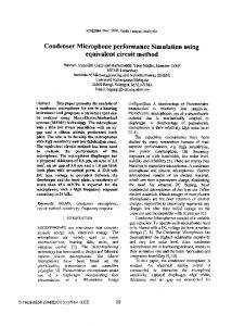
using the Partial Element Equivalent Circuit (PEEC) method which ... Modified Nodal Analysis (MNA) method [5]. For- ... proximation used for the circuit elements.
Application of the Partial (PEEC) method to realistic Albert
Elemerit Equivalent Circuit printed circuit board problem Andreas
E. Ruehli
IBM Research Division Yorktown Heights, NY 10598
Abstract
In this paper we give an example of the analysis of a printed circuit board problem which is quite complicated. The board is populated with three wires where two of them extend outside of the board to represent off board coupling. This problem is solved using the Partial Element Equivalent Circuit (PEEC) method which is a circuit based mixed potential integral equation (MPIE) solution technique. This technique is capable of solving heterogeneous circuits and fields problems in both the time and the frequency domains. We show that the time domain can be used to isolate some of the sources of radiation. Also, the example problem shows surprising results with respect to the coupling of signals on the printed circuit board.
1
Introduction
In this application paper we describe a printed circuit board problem which is solved using the Partial Element Equivalent circuit (PEEC) method. This method is a full wave technique for the solution of heterogeneous, mixed circuit and fields problems. To illustrate the uniqueness of our solution method we have chosen to solve the problem in the time domain. Our solver code is an experimental program and so far data entry is non-trivial for large problems. This is one of the reasons why we are ignoring the dielectric layer on the printed circuit board even though the technique can handle dielectrics as is shown in Section 2. Here, we want to explore the capabilities of the approach for a complex structure and to show some of its advantages in comparison with the other approaches demonstrated in this session. Our non-commercial full wave time domain solver is an experimental program which is based on* the (PEEC) technique e.g. [I, 21. The fact that this ap0-7S0~-501~-~/~S/$10.00 0 199X IEEE
C. Cangellaris
University of Illinois Urbana, IL 61821
preach is quite flexible is illustrated by the different problems which have been solved using PEEC e.g. [3]. The fundamental idea of the PEEC method is to convert the MPIE into the circuit domain so that a mixed EM-circuit problem can be handled exclusively in the circuit domain. Our implementation has been extended to include delays for both the time and the frequency domain. This is quite different from the original quasi-static PEEC models which are extensively used today to analyze packages. For the quasi static case, we could use conventional circuit solvers like ASTAP [4]. The b asic formulation of the circuit equations in most modern circuit solvers is the Modified Nodal Analysis (MNA) method [5]. Fortunately, the same basic formulation technique can be used for the new code. Another challenge for using delays in the time domain is the stability issue. Unfortunately, the stability in the time domain can introduce considerable difficulties especially for problems with fast transient input waveforms. This is why the method had been applied mostly to problem where Gaussian input waveforms could be utilized e.g. [6]. W e used some of the stabilization techniques given in [7] to obtain stable time solutions. This approach has enhanced the stability of the solution in the time domain. Another issue is the time integration of the resultant delay differential equations. Continuous progress has been made in this area [S].
182
Here, we apply the technique to the very interesting challenge problem which has been devised for this session. It is an extension of an earlier model which was designed to estimate the impact of off board traces. The circuit board problem which is solved in this paper is 25 cm x 25 cm as is shown in Figs. 1 and 2. More details of the geometry will be given in Section 3. Note the interesting fact that both off board traces involve directional coupling. However, the trace which
Figure 2: Side view of printed
lr Figure 1: Top view of printed
circuit
problem
/lo
4 0
circuit
problem
fans out to the top involves forward coupling to the active trace while the lower trace to the left has backward coupling to the active trace. This is one of the reasons why the results are quite different. In Section 2, we give some insight into the PEEC Figure 3: Center part of board model. Then, we consider the coupling for partial inductances in the time domain and some of the apcharges for the dielectrics with E, > 1 separately from proximation used for the circuit elements. In Section the displacement currents due to the free charges. We 3, more details are given about the specific problem start from the sum of all the sources of electric field to be solved. Finally, in Section 4 very interesting reat any point in space sults obtained from the transient analysis for several J(i;, t) + &qF, t) points in the problem. &(e,t) = --y& + W(FJ) . (2.1)
0 3
where ,!?cis a potential applied electric field, J is the current density in the conductors, ii and 4, are vector and scalar potentials, respectively. As indicated above, the dielectric areas are taken into account as a In this section we briefly describe the key aspects of current rather than a capacitance through the scalar the PEEC time domain solution technique used. potential. This is accomplished by adding and subtracting ~0% in the Maxwell equation for a, or 2.1 Mixed Potential Integral Equation
2
Partial element equivalent cuit time domain solution
cir-
We give an abbreviated derivation of the PEEC model which includes finite size dielectric regions besides the conductors or wires [9]. The starting point is the PEEC model for conducting objects and some of the work on dielectrics for the MOM. We specifically concentrate on approximations of the currents, charges and potentials (voltages) which are appropriate for an equivalent circuit representation. The key idea is to treat the displacement current due to the bound 153
Here, the current in Eq. 2.2 is written as a total current
where &(~,t) is the conductor current and the remainder of the equations is the equivalent polarization current due the the dielectrics.
The vector potential A is for a single conductor at the field point e given by A(?, t) = j.i s,, G(?, n)@/, where the retardation
td)dv/
Voltage [V] I
1-I.O:VI .. ....... . . .. T2.0:V I
-
(24
time is given by
td = t _ I 7 - 3 I C -1.00
which simply is the free space travel time between the points f and PI. It is noted that in the formulation derived here, both the retardation and the Green’s functions are free space quantities where
2.2 Finally, using the above we can formulate the mixed potential integral equation for the electric field at a point 7 which is to be located either inside a conductor or inside a dielectric region. Starting from Eq. 2.1 with the externally applied electric field set to zero, and substituting for A and 9 from Eq. 2.4 and Eq. 2.7 respectively
,LL G(f, 7,) “‘;; s VI
+
EO(G
-
l>p s
+7E. s v, G(c,
VI
tr)q(r/,
Coupling
Lp,p
d2E(F/,
at load point
2
and time
doniain
solution
1
= l-Idv,dvp. 47r a,ap ssvp vp R
.
(2.9)
Using this definition, and approximating the’exponential term by using the center to center distance for R, the partial inductance coupling can be rewritten as
t(j)
at2
td)dvl = 0.
-I- Ins1
IO.00
The coupled circuit elements, which correspond to the inductive and capacitive coupling, play a key role in the PEEC model. Here, we only look at the inductive coupled elements for brevity. Partial inductances are involved in Eq. 2.8 for both the magnetic coupling as well as the field interaction at the dielectric layer. After discretization of Eq. 2.8, the second term can be recast in the form of partial inductances
td)d~,
G(F, 3)
5.00
leads to Kirchoff’s current law which is inherent in the modified nodal analysis (NMA) circuit equation formulation utilized. More details are found in the references.
The scalar potential is similarly
+
_ ___..
Figure 4: Voltages
P-6)
Y(F, t) u
- ..-. -1 0.00
(2.8)
Note that Eq. 2.3 is used for the total current in both the conductors and the dielectrics. In the PEEC formulation this equation is converted into an equivalent circuit, where both currents J and charge q or the corresponding potentials * are the unknowns. The two unknowns, j and q, are each expanded into a series of pulse basis functions which are also used for as the testing functions. The application of the orthogonal testing functions leads to the PEEC circuit in terms of partial inductances L,, coefficients of potential P, resistors R and delays d where the delay is due to the distances between the Lp’s and the potential coefficients P. Also, the continuity equation V . I+ jwq = 0 must be satisfied which
jwLp&,
+ jwLp,plpe-3PR@
(2.10)
Where the partial self inductance of the cell cy is represented by the first term and were the second term represents the inductive coupling to cell ty from a current in cell ,B. The delay between cells cy and /3 are given by the phase term e -joRap where again Rap is the center to center distance between cells a and p. In the time domain we have a corresponding delay equation (2.11) -baa&(t) + -b&(t - 7-1
184
where T is the physical delay. The Laplace transform can b6 used to show the correspondence between the two cases.
Amplitude
Voltage [V] x 1Om3 ~00~00 i ..,..-- -.-----------r-------
3 1e-01 3
400.00
^
300.00
.-
200.00
-
/\ i 1. I i \ L,., \ ,/
.__= i T,.*:V, . ....... . .. -- T2.O:V I .-
1 e-02 3 1e-03 3 le-04
---- --..---..1e+02
-.- ..___-__ 3
Figure 5: Spectra
:j’.,\., -: le+O3
----l--m
at load point
F [MHz]
3
2
--L---
-_I
0.00 5.00 10.00 Figure 6: Voltages at upper wire
T [nsl
It is evident that in the frequency domain the cou- is driven by a voltage source. A more detailed view pling term in Eq. 2.10 will enter into the circuit ma- of the center part is shown in Fig. 3. The active wire trix with the appropriate exponential. This is quite in in the middle has a source at Point 1 with 10 Ohms contrast to the case for the time domain. There, the in series and with rise and fall times of 0.3 ns. The MNA equations can be written which is an extension on-switching ramp starts at 0 ns with an amplitude of the usual form to the delayed case, or of 1 V. The off switching ramp starts a 3.85 ns and the total input duration is 10 ns. Hence, the input is (2.12) zero from 4.15 ns to 10 ns. Terminations are placed at c G; y(t - 7;) + c Ci jl(t - 7;) = h(t). i=o i=o the other three nodes shown in Fig. 3. Importantly, where 70 = 0. Equation 2.12 is solved using a small we chose two different ways to terminate the wire at time step h which is smaller than most of the delays point 2 to illustrate two cases. For case 1 we leave +ri. This changes the usually dense circuit matrix to the Point 2 open while for case 2 we terminated the sparse, while most of the coupling terms will be evalu- wire with 50 Ohms in parallel with 1 pF. Both ends ated as entries into the right hand side. This changes of the other two wires, Points 3 and 4, are terminated the run time for the time domain code to hopefully with 50 Ohms. To model the structure, we chose a cell size of 1.25 less than O(n2) leading to a significant improvements cm which corresponds to 20 cells/X at 1.2 GHz. Howin run time. ever, near the wires, the width cell size was reduced by another factor 10 to take care of the local current 3 Outline of printed circuit prob- distribution in the board groundplane. The width of the geometrical details like the cut in the board etc. lem are adjusted to fit within the basic 1.25 cm cell size. The problem consists of three wire or traces on a printed circuit board which is 25 cm long and 25 cm Results of computer experiwide as is shown in Figs 1 and 2. The wires are 0.2 4 mm wide with 0.2 mm spacing and all the copper ments layers are 0.02 mm thick with the resistivity of 1.74 10e8 Ohm m. The two outside wires extend over the In the MNA based PEEC formulation we can investiedge by 15 cm each where the upwards pointing wire gate voltages and currents anywhere in the electronic is 15 cm long while the downward pointing wire is 80 circuits. Currents and potentials are also automaticm long. The left trace and the center trace overlap cally computed for the geometry parts. Voltages in for only 5 cm while the right trace is parallel to the the geometrical part are simply potential differences, center trace for 12 cm. The problem is designed to where ,J = 91 - $2. Further, we also can output all represent a board with connecting wires. Both wires the currents through the cells into which the conducwhich extend outside of the board are passive in that tors are subdivided. Hence, all results are obtained they do not have active sources while the center trace with a single run. However, since we are showing re-
Amp1 i tude 2 r- ------. -I---__ -le-01 i................ 5
2 le-02 5
2 le-03 5
--
--._. _.- ._.__.-- i-.‘~T,.O:“* -1, $~:‘~~~~
._
1
:-
...(
.-
Tl.O:VI ... . T2.0:Vl
,.
._.
i:.. L: :..le+O2
3
Figure 7: Spectra
I..&.--..---‘-3 I#03
at upper
-300.00 -2---.-!--------.-~--.---.--~-. 0.00
3 ._.. T [nsl 5.00 10.00 Figure 8: Voltages for left wire
F [MHz] 3
wire
sults for two different input waveforms we had to do two runs. The total number of unknowns is 5830. The transient analysis step took 31 Minutes for an analysis time of 10 ns and 4 minutes for the calculation of the partial inductances and the coefficients of potential on an IBM RS/GOOOmodel 595 workstation. Here, we analyze a few time signals for the printed circuit board example problem. In fact, several very interesting new results and insights can be gained from the time domain analysis presented here. For all the time and spectrum results, we give a comparison without a load at node 2 (case 1, Truce 1) in contrast to the case with a resistor and capacitance load at node 2 (c&se 8, Truce 2) . The first set of waveforms are evaluated at the end of the driven wire at point 2 in Fig. 3 where the potential load may be connected. The waveforms for cases 1 and 2 are given in Fig. 4. As expected, the loaded waveforms are much smaller than the unloaded case which leads to several reflections due to the low damping in the loop. The corresponding spectra which are given Fig. 5 show the reduction in the spectral amplitude. From this we could expect that most signals are more quiet, with a lower spectrum, for case 2. The next point we investigate is at the upper edge of the board. Specifically, we look at the voltage between the upper wire and ground located at the edge of the card directly below the wire which is due the the coupling from the center wire. We note that the coupled signal in Fig. 6 even changes polarity early on due to the change in the load. As expected, the large change in the coupled waveforms also leads to a large change in the spectrum shown in Fig. 7. Even more interesting results are obtained for the wire which leaves the board at the left hand side. Again, to observe the signal which is feed into the off board wire, we measure the voltage at the board edge. 186
Amplitude
_-
-Tl.O:Vl . I .... .. ... .. T2.0:V 1
le-01 3 le-02 3 1e-03 3 1e-04 3 le+02
3
Figure 9: Spectra
le+03
3
--
T [nsl
at left wire
The behavior of the waveforms in Fig. 8 for the two cases seem to change to a much different frequency content. For this wire, the coupling section is only 5 cm. The open driven line changes from a larger voltage to a larger current due to the termination. As expected the different waveforms have quite a different main frequency and amplitude content which is shown in the spectra Fig. 9. A similar difference in the spectra can be observed in the upper trace. However, the change in the spectra is quite unpredictable since the signal with the loads shows an amplitude increase for some of the higher spectral frequencies. Finally, we want to investigate the impact of the gap in the ground plane. Hence, we inspect the voltage across the gap which forms a slot antenna. Fig. 10 shows what the voltage across the gap right under the left signal wire seems to have a component above 1 GHz. Surprisingly, the quite dissimilar waveforms have about the same frequency content in their spectra Fig. 11 at about 1.2 GHz. An interesting question is if the leads tdradiation from the gap in the ground.
References
Volage [V] x 10e3 30.00
“-7Tl.O:Vl ; $5:‘ii’:“i;i’r”’
’
20.00
-20.00
II
,.
”
[11
.:
_
”
.: 1 I I
-30.00
5.00 o.bo Figure 10: Voltages
10.00 across gap
T [nsl
Amplitude _,TI.O:VI ..................... T2.0:V I
3 I e-03 ,...,.,...”
3 I e-04
W. Pinello, A. C. Cangellaris and A. E. Ruehli. Hybrid electromagnetic modeling of noise interactions in packaged electronics based on the partialIEEE element equivalent circuit formulation. Transactions on Microwave Theory and Techniques, MTT-45(10):1889-1896, October 1997.
PI G.Antonini,
S. Cristina, A. Orlandi. PEEC modeling of hight voltage tower under direct and nearby lightning strike. In Proc. 10th Int. Symp. on High Voltage Eng. ISH, volume 10, Montreal,CA, August 1997.
141W.
T. Weeks, A. J. Jimenez, G. W. Mahoney, D. Mehta, H. Quasemzadeh and T. R. Scott. Algorithms for ASTAP - a network analysis program. IEEE T ransactions on Circuits Theory, CT-20( 11):628-634, November 1973.
3 1 e-05
\ -2
_. _ I e+O2
3
Figure 11: Spectra
5
A. E. Ruehli. Equivalent circuit models for three dimensional mult’lconductor systems. IEEE Transactions on Microwave Theory and Techniques, MTT-22(3):216-221, March 1974.
_._” .-. .--.-.
-;---
F [MHz]
1e+03
accross
gap
PI C. Ho, A.
Ruehli, P. Brennan. The modified nodal appr. to netw. anal. IEEE Transactions on Circuits and Systems, pages 504-509, June 1975.
Conclusions
PI B.P.
Several observations can be made about the new time domain solution results in this paper. Our experimental PEEC based program is very well suited for the solution of time domain problems. First, the time solution has several advantages in that the signals source can be represented by correct time domain waveforms. Hence, the input spectra are correctly represented and the output spectra correspond to the actual situation where the contribution of each source is appropriately weighted. Also, surprising is how the different wire and ground geometries filter the signal spectra. They form rather sophisticated microwave filters. The printed circuit board designer is not aware of the complicated interactions of the board wires. %‘e were able to identify by this analysis where some of the frequencies are generated. This analysis helps toedesign better printed circuit boards which do not exhibit these coupling behaviors. This in turn should lead t.o reduced coupling and EM1 radiation. lS7
Rynne. Comments on a stable procedure in calculating the transient scattering by conducting surfaces of arbitary shape. IEEE Transacti’ons on Antennas and Propagation, APP-41(4):517-520, April 1993.
PI J.Garrett,
A. E. Ruehli, C. Paul. Recent improvement in PEEC modeling accuracy. In Proc. of the IEEE
Int. Symp. on Electromagnetic
ity, Austin,TX,
Compatibil-
August 1997.
PI A.
E. Ruehli, U. Miekkala, A. Bellen, H. Heeb. Stable time domain solutions for EMC problems using PEEC circuit models. In Proc. of the IEEE Int. Symp. on Electromagnetic ity, Chicage,Ill, August 1994.
PI A.
Compatibil-
Circuit models Ruehli and H. Heeb. for three-dimensional geometries including dielectrics. IEEE Transactions on Microwave Theoy and Techniques, 40(‘7):1507-1516, July 1992.