A 32-element 8-bit photonic true-time-delay system ... - IEEE Xplore
Recommend Documents
AbstractâPhotonic crystal slab waveguides (PCSWs), based on the novel ... The PCSWs possess fundamental bandgaps for even. (transverse-electric (TE)-like) ...
Jun 11, 2013 - Later, a high negative dispersion of Ð212 ps/nm/km and âD of $11 ps/nm/km over E Ñ S Ñ C Ñ L Ñ U wavelength bands was obtained with a ...
Photonic Metamaterials: Magnetism at. Optical Frequencies. Stefan Linden, Christian Enkrich, Gunnar Dolling, Matthias W. Klein, Jiangfeng Zhou, Thomas ...
Yao, Frankie Liu1, Dinesh Patil1 , Philip Amberg1, Nathaniel Pinckney1, Po Dong2, Dazeng Feng2, Mehdi. Asghari2, Attila Mekis3, Thierry Pinguet3, Kannan ...
A.M.J. Koonen (1), H.P.A. van den Boom (1), H.-D. Jung (1), H. Yang (1), E. Ortego Martinez (2),. P. Guignard ... and bus or star-bus ones for larger buildings. 1.
frequency signal (RF) and the local oscillator signal (LO) are applied to the first .... where Ein and !c are the amplitude and the angular frequency of the optical ...
Apr 20, 2012 - Abstract: A photonic free-electron laser (pFEL) produces coherent Cerenkov radiation from a set of parallel ... consequently, coherent radiation can build up. The frequency of ... enhance the power available in the THz domain.
James C. Gates, and Peter G. R. Smith ..... Emmerson, C. B. E. Gawith, S. P. Watts, R. B. Williams, P. G. R. Smith, S. G. McMeekin, J. R. Bonar, and R. I. Laming,.
Oct 14, 2011 - The total optical power at the idler wavelength Ñ IdlerЮ oscillates as a ... (e) This idler has power oscillates with RF signal frequency and can ...
Nov 22, 2012 - AbstractâIn the typical Power over Ethernet (PoE) system, the ... gram under Grant 2011C21056, and in part by the Power Electronics Science.
Ji Fang Tao, Hong Cai, Yuan Dong Gu, Jian Wu, and Ai Qun Liu. AbstractâA photonic ... using photonic waveguide-based Michelson interferometer (MI),.
AbstractâThe orientation dependent characteristics of the four-layered hexagonal lattice structure of a photonic crystal fiber (PCF) have been investigated and ...
1Semiconductor Photonics Group, Department of Physics, Trinity College Dublin, ... 3Institute of Physical Chemistry, University of Hamburg, Grindelallee 117, ...
2, MARCH/APRIL 2015. 9000105. Thickness-Dependent ... Republic of China (Taiwan) under Grant NSC-100-2112-M-003-005-MY3. H.-T. Hsu is with the ...
Incorporation of a photonic layer at the metallization levels of a. CMOS circuit. JM. Fedeli a, M.Migettea, L.Di Cioccio a, L.El Melhaoui a, R. Orobtchouk b, ...
Jun 26, 2013 - J. Michel, and L. C. Kimerling, BDemonstration of a tunable ... [14] J. Capmany, D. Pastor, A. Martinez, B. Ortega, and S. Sales, BMicrowave ...
by adjusting the bias of DDMZM to compensate the dispersion induced ... (DC) bias of the modulator, which is different from those approaches that using MZI ...
AbstractâThis paper reports the theoretical and experimental investigations of the strain-induced resonant wavelength shift effect of a modified single-defect ...
May 30, 2013 - parallel (not cascaded) MZI slicers with coupled and modified weight coefficients as compared to ... When this HB-FLM is used as a slicer in an.
Manuscript received June 1, 2014; revised August 15, 2014; accepted August ..... [25] C. M. Nelson, M. Spies, L. S. Abdallah, S. Zollner, Y. Xu, and H. Luo,.
Feb 17, 2011 - Ali Mostafavi, Student Member, IEEE, Dulcy M. Abraham, Daniel ... A. Mostafavi, D. M. Abraham, and J. Sinfield are with the School of Civil.
people find friends whose personality and characteristics have been voted to suit them well by their social network. MatchMaker also encourages more TV ...
When the crosstalk cancellation filters are time in- variant, head rotations cause the perceived position of virtual sound sources to shift towards the loudspeakers' ...
Feb 17, 2011 - Ali Mostafavi, Student Member, IEEE, Dulcy M. Abraham, Daniel DeLaurentis, ... AbstractâThe objective of this paper is to propose an analysis.
A 32-element 8-bit photonic true-time-delay system ... - IEEE Xplore
is the ability to obtain large-element number and high bit accuracy true-time delays (TTDs) in ... excess loss. The recent development of two-dimensional micro-.
IEEE PHOTONICS TECHNOLOGY LETTERS, VOL. 15, NO. 6, JUNE 2003
849
A 32-Element 8-Bit Photonic True-Time-Delay System Based on a 288 288 3-D MEMS Optical Switch Volkan Kaman, Member, IEEE, Xuezhe Zheng, Member, IEEE, Roger J. Helkey, Senior Member, IEEE, Chandrasekhar Pusarla, and John E. Bowers, Fellow, IEEE
Abstract—A large-scale three-dimensional microelectromechanical-system optical switch is used for the first time to realize a true-time-delay (TTD) beamformer for phased-array radar applications, with a capacity of 32 antenna elements and eight bits of delay. The 288 288 optical switch has a median loss of 1.4 dB and all measured 82 944 paths exhibit less than 2.3 dB loss at 1310 nm. The TTD beamformer exhibits a loss variation of 1.5 dB, which is equalized using a mirror-offset technique. Index Terms—Array signal processing, microelectromechanical devices, microelectromechanical system (MEMS), optical fiber delay lines, optical switches, phased-array radar.
I. INTRODUCTION
A
N IMPORTANT element of wide-band phased-array radar is the ability to obtain large-element number and high bit accuracy true-time delays (TTDs) in a low-cost, small, and light volume with minimal signal degradation. Current all-electronic TTD systems based on microwave components suffer from high signal loss and dispersion as well as large size and weight. On the other hand, due to their low loss and low dispersion, optical fibers are ideal photonic delay lines. In the past decade, several photonic TTD beamformers have been demonstrated with some of the more popular techniques being based on tunable lasers with dispersive fiber delay lines [1], [2] or fiber grating prisms [3], [4], integrated optical switches [5]–[7], or a white cell [8]. The performance of optically switched TTD units based on integrated waveguides has traditionally been limited by the high fiber-to-waveguide coupling losses, high polarization-dependent losses (PDLs), and a broad loss variation for different paths. Furthermore, the relatively small switching size (up to 8 8) of waveguide-based switches requires a cascaded-switch TTD system architecture for achieving high bit accuracy per element of delay, which not only augments the optical loss limitations, but also increases the number of switches and overall cost, size, and control of the TTD system. In order to realize a large and compact TTD system with a capacity for 32 antenna elements and eight bits of delay, it is desirable to increase the optical switch size without introducing excess loss. The recent development of two-dimensional microelectromechanical-system (2-D MEMS) switches has resulted Manuscript received January 28, 2003; revised March 7, 2003. This work was supported by The Defense Advanced Research Project Agency SPO Office. The authors are with Calient Networks, Goleta, CA 93117 USA (e-mail: [email protected]). Digital Object Identifier 10.1109/LPT.2003.811348
Fig. 1. Measured loss distribution (including connector losses) of the 288 288 3-D MEMS optical switch. The median loss is 1.4 dB at 1310 nm.
2
in lower optical losses (maximum 3.1 dB) with switch sizes up to 16 16 [9]. However, since the number of switching ele, there is a practical limit ments and electrical drivers scale as in the achievable switch size with 2-D MEMS-based switches. On the other hand, the developments in 3-D MEMS (with a switching elements) have allowed superior scaling of only the demonstration of much larger switches, with recent switch sizes beyond 200 ports [10], [11]. In this letter, we present and demonstrate, for the first time, variable TTD beamforming for wide-band phased-array radar applications using a low-loss 288 288 3-D MEMS based optical switch. II. 3-D MEMS OPTICAL SWITCH CHARACTERISTICS The 288-port optical switch is based on 3-D MEMS technology for large port counts and compact size. The light from an input fiber is collimated and incident on a MEMS mirror which can deflect light onto any of the output MEMS mirrors. The output mirror then aligns the optical beam onto a particular output collimator. For low-loss coupling, the position and angle of the beam must be aligned with the collimator, which re-switching elements for an -port switch. The single quires crystal structure and the flatness of the bulk MEMS allow for excellent mechanical properties and very low optical loss over 288 optical switch has a wide wavelength range. The 288 a median loss of 1.4 dB at 1310 nm and the measured loss is shown in Fig. 1. All 82 944 paths exhibit less than 2.3-dB loss, which also includes connector losses. The switch also has
IEEE PHOTONICS TECHNOLOGY LETTERS, VOL. 15, NO. 6, JUNE 2003
TABLE I THE NUMBER OF SWITCHING ELEMENTS AND OPTICAL LOSSES INCURRED FOR REALIZING A SINGLE-ELEMENT AND 8-BIT RESOLUTION TTD SYSTEM USING VARIOUS SIZE OPTICAL SWITCHES ARRANGED IN THE MINIMUM LOSS CONFIGURATION
TABLE II THE MAXIMUM NUMBER OF INPUT ELEMENTS THAT CAN BE SUPPORTED WITH A SINGLE 288-PORT OPTICAL SWITCH WITH 8-BIT RESOLUTION
2
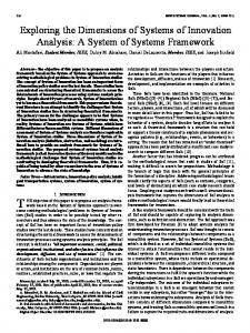
Fig. 2. (a) Single-element 8-bit resolution TTD unit based on 2 2 switches and a binary delay architecture with a typical maximum loss of 12.6 dB. The delays are , 2 , 4 , 8 , 16 , 32 , 64 , and 128 . (b) A 32-element 8-bit resolution TTD unit based on a 288 288 switch and a binary delay architecture with a typical maximum loss of 12.6 dB. The delays are , 2 , 4 , 8 , 16 , 32 , 64 , and 128 . (c) Single-element 8-bit resolution TTD unit based on a 288 288 switch and a linear delay architecture with a typical maximum loss of 2.8 dB. The delays are , 2 , 3 , 4 , . . ., 253 , 254 , and 255 . (d) An eight-element 8-bit resolution TTD unit based on a 288 288 switch and a pseudobinary delay architecture with a typical maximum loss of 5.6 dB. The delays are , 2 , 3 , . . ., 8 , 16 , 24 , . . ., 56 , 64 , and 128 .
2
2
2
a wide transparent optical bandwidth from 1260 to 1625 nm with a loss variation of less than 1 dB. The measured median PDL is 0.07 dB with a maximum of 0.3 dB. Due to the design of the switch, chromatic dispersion ( 0.1 ps/nm) and polarization-mode dispersion ( 10 fs) are negligible and degradation of the radar signal would not be expected for frequencies well beyond 40 GHz. The switch is also capable of handling optical input powers beyond 13 dBm as well as providing stable loss over a wide range of environmental conditions. The excellent optical properties of the 288-port switch ensure minimal signal degradation and a high signal-to-noise ratio. Typical measured mirror switching times are less than 10 ms. III. TTD CONCEPT A TTD system with a capacity for 32 antenna input elements and 8-bit accuracy can be constructed with several different size optical switches. To simplify the comparisons of systems with different switch sizes, we assume a size-independent loss of 1.4 dB, which is reasonably accurate (1 dB for a 2 2 switch [9], 3.1 dB for a 16 16 switch [9], and 1.4 dB for a 288 288 switch). For a single input element and 8-bit resolution system constructed with 2 2 switches, as shown in Fig. 2(a), a binary delay architecture (with delays of , 2 , 4 , 8 , 16 , 32 , 64 , and 128 ) requires a cascade of eight switches with a maximum loss of 12.6 dB. On the other hand, the same bit accuracy and binary delay architecture can be implemented using a single 288 288 switch [Fig. 2(b)]. The minimum delay for the 288-port switch architecture is achieved with the input sending the optical
signal straight to the output with a loss of 1.4 dB. For longer delays, additional passes through the switch are used for each extra bit of delay, which results in increased loss of 1.4 dB per pass (with a 12.6-dB typical loss for the worst case delay). In order to keep the loss the same for all delay values, the MEMS mirrors can be detuned from optimum alignment to increase the loss when using lower loss delay values, which is experimentally demonstrated in the next section. The TTD system based on a 288-port switch is able to support all 32 input elements using a single switch while a total of 288 2 2 switches would be required to realize the same capacity. Additionally, large-scale optical switches also allow for an architecture where the delays are in linear increments rather than binary increments, resulting in reduced losses per input element. As shown in Fig. 2(c), a , 253 , 256 256 switch with linear delays of , 2 , 3 , 254 , and 255 would support a single input element for 8-bit resolution with a maximum loss of 2.8 dB. However, this low loss is achieved at the expense of 32 256-port switches in realizing a 32-element TTD system. It is also possible to trade off the number of large-scale switches and optical loss between the linear and binary delay limits by using a pseudobinary delay architecture. A 16-element switch with 8-bit resolution would require 16 delay lines (with delays of , 2 , 3 , , 8 , 16 , 24 , , 56 , 64 , and 128 ) and a maximum loss of 5.6 dB per element [Fig. 2(d)]. The number of optical switches required in realizing a single-element TTD system based on various switch sizes is summarized in Table I, using a configuration to minimize optical loss for each switch size. Large optical switches can significantly reduce the optical loss, but require a substantial number of delay fibers for minimum loss. A large switch also allows a tradeoff between the loss and complexity to achieve a 32-element 8-bit TTD system, with linear delay for minimum loss, binary delay for minimum number of fiber delays, and a variety of pseudobinary delay sequences between these two limiting cases (Table II).
KAMAN et al.: A 32-ELEMENT 8-BIT PHOTONIC TTD SYSTEM BASED ON A 288
Fig. 3. Measured optical delays on a high-speed oscilloscope. The loss variation is 1.5 dB while the path delay accuracy is within 0.15 ns.
IV. EXPERIMENTAL RESULTS The 288 288 nonblocking 3-D MEMS switch (Fig. 1) was used to demonstrate the concept of a 32-antenna element, 8-bit TTD system, as shown in Fig. 2(a). The 1-ps output of a 20-MHz repetition rate 1550-nm short pulse source was split into 32 individual channels using two 1 : 16 optical splitters. These 32 channels at a peak pulse power of 3 mW were then fed into the input ports of the switch. For this demonstration, five different length optical fibers were connectorized and looped around the switch, with lengths equaling delays of 0.5, 1, 2, 4, and 8 ns. The switch outputs were then captured on a high-speed oscilloscope with respect to an attenuated reference point after a single bit of delay for each input (Fig. 3). The measured median delay error is less than 0.15 ns, which is due to varying internal switch fiber lengths and nonoptimal fiber splicing lengths. We estimate that a median delay error of less than 10 ps is possible. As the optical paths within the switch have a loss distribution as shown in Fig. 1, the optical pulses for each delay line have different optical peak powers varying by 1.5 dB (Fig. 3). Additionally, the optical delay lines were connectorized, which added an extra loss to each path. This loss can be minimized once the delay lines are directly spliced to the internal switch fibers. In any case, the variability of the optical loss per path can be compensated by slightly misaligning the mirrors to introduce some additional loss. Hence, each path can be set to a specific optical loss at the output of the switch without requiring external variable optical attenuators. Fig. 4 shows the experimental results of offsetting the output mirror of a path to achieve different optical output powers. A dynamic range of 20 dB with 0.1-dB accuracy can be achieved with this technique and ensures constant output powers for the 32-element, 8-bit TTD system based on 3-D MEMS switch. V. CONCLUSION A compact and low-loss 288 288 3-D MEMS optical switch with negligible dispersion has been used for the first
288 3-D MEMS
851
Fig. 4. Receiver response to an optical pulse demonstrating optical loss equalization in the optical switch by misaligning MEMS mirrors.
time to generate TTDs for phased-array radar applications. Large-scale optical switches have the advantage of lower loss and high switching density for reducing components and realizing high input element TTD systems with high bit accuracy. Additionally, employing 3-D MEMS for the switching technology allows for optical output equalization by misaligning the mirrors. REFERENCES [1] R. Soref, “Optical dispersion technique for time-delay beam steering,” Appl. Opt., vol. 31, pp. 7395–7397, 1992. [2] M. Y. Frankel and R. D. Esman, “True time-delay fiber-optic control of an ultrawideband array transmitter/receiver with multibeam capability,” IEEE Trans. Microwave Theory Tech., vol. 43, pp. 2387–2394, Sept. 1995. [3] H. Zmuda, R. A. Soref, P. Payson, S. Johns, and E. N. Toughlian, “Photonic beamformer for phased array antennas using a fiber grating prism,” IEEE Photon. Technol. Lett., vol. 9, pp. 241–243, Feb. 1997. [4] J. Yao, J. Yang, and Y. Liu, “Continuous true-time-delay beamforming employing a multiwavelength tunable fiber laser source,” IEEE Photon. Technol. Lett., vol. 14, pp. 687–689, May 2002. [5] W. Ng, D. Yap, A. Narayanan, and A. Watson, “High-precision detectorswitched monolithic GaAs time-delay network for the optical control of phased arrays,” IEEE Photon. Technol. Lett., vol. 6, pp. 231–234, Feb. 1994. [6] E. J. Murphy, T. F. Adda, W. J. Minford, R. W. Irvin, E. I. Ackerman, and S. B. Adams, “Guided-wave optical time delay network,” IEEE Photon. Technol. Lett., vol. 8, pp. 545–547, Apr. 1996. [7] K. Horikawa, I. Ogawa, T. Kitoh, and H. Ogawa, “Silica-based integrated planar lightwave true-time-delay network for microwave antenna applications,” in Tech. Dig. OFC’96, 1996, pp. 100–101. [8] B. L. Anderson and R. Mital, “Polynomial-based optical true-time delay devices with microelectromechanical mirror arrays,” Appl. Opt., vol. 41, pp. 5449–5461, 2002. [9] P. de Dobbelaere, K. Falta, L. Fan, S. Gloeckner, and S. Patra, “Digital MEMS for optical switching,” IEEE Commun. Mag., vol. 40, pp. 88–95, Mar. 2002. [10] R. Helkey, S. Adams, J. Bowers, T. Davis, O. Jerphagnon, V. Kaman, A. Keating, B. Liu, C. Pusarla, D. Xu, S. Yuan, and X. Zheng, “Design of large, MEMS-based photonic switches,” Opt. Photon. News, pp. 43–45, 2002. [11] V. A. Aksyuk, S. Arney, N. R. Basavanhally, D. J. Bishop, C. A. Bolle, C. C. Chang, R. Frahm, A. Gasparyan, J. V. Gates, R. George, C. R. Giles, J. Kim, P. R. Kolodner, T. M. Lee, D. T. Neilson, C. Nijander, C. J. Nuzman, M. Paczkowski, A. R. Papazian, R. Ryf, H. Shea, and M. E. Simon, “238 238 surface micromachined optical crossconnect with 2 dB maximum loss,” in Tech. Dig. OFC 2002, 2002, Postdeadline Paper PD-FB0.