A 60fps 496mW Multi-Object Recognition Processor with Workload-Aware Dynamic Power Management Joo-Young Kim, Seungjin Lee, Jinwook Oh, Minsu Kim, and Hoi-Jun Yoo School of EECS, KAIST, 373-1, Guseong-dong, Yuseong-gu, Daejeon, 305-701, KOREA
[email protected] ABSTRACT An energy efficient object recognition processor is proposed for real-time visual applications. Its energy efficiency is improved by lowering average power consumption while sustaining high frame rate. To this end, the proposed processor features from all levels of chip design. In architecture level, it performs 3-stage task pipelining for high frame rate operation and workload-aware dynamic power management for low power consumption. In block level, energy efficient special purposed engines are employed while software controlled clock gating is exploited for fine-grained clock control. In circuit level, analog-digital mixed design is used to reduce power with the same performance. As a result, the 49mm2 chip in a 0.13μm technology achieves 60fps object recognition for VGA (640x480) input with 496mW power at the supply of 1.2V. It means only 8.2mJ is dissipated per frame, which is 3.2X more energy efficient than the state of the art.
Categories and Subject Descriptors C.1.2 [Multiprocessors]: parallel processors I.4.8 [Scene Analysis]: object recognition
General Terms Algorithms, Design, Management, Performance
Keywords Multimedia processor, energy efficient object workload-aware dynamic power management
recognition,
1. INTRODUCTION Object recognition becomes a key technology for advanced visual applications such as autonomous cruise control, intelligent robot vision, and surveillance system [1-3]. Basically, most conventional object recognition mechanisms are performed by following algorithm sequences [4]. Firstly, various scale spaces for input video stream are generated by a cascade filtering approach and feature points are extracted among them using local maximum search. Then, the extracted feature points are converted to descriptor vectors that describe magnitude and orientation characteristics of them. Lastly, the final decision is made by performing nearest neighbor matching with pre-defined database composed of more than ten thousands of object vectors. Since each stage of object recognition includes Permission to make digital or hard copies of all or part of this work for personal or classroom use is granted without fee provided that copies are not made or distributed for profit or commercial advantage and that copies bear this notice and the full citation on the first page. To copy otherwise, or republish, to post on servers or to redistribute to lists, requires prior specific permission and/or a fee. ISLPED’09, August 19–21, 2009, San Francisco, California, USA. Copyright 2009 ACM 978-1-60558-684-7/09/08...$10.00.
considerable amount of computations, it is hard to achieve real-time operation. However, to apply it to the real-time visual applications aforementioned, a high frame rate operation, for example over 30fps, is demanded. In addition, low power operation is also required for battery limited applications such as mobile robot or handset device. To reduce computational complexity of conventional object recognitions, the processor of [2] introduced visual attention paradigm to object recognition hardware. With cellular neural network based visual attention engine [5], it reduces internal workload of object recognition by filtering meaningless feature points. Although it achieves real-time operation, however, it has not fully considered energy efficiency in terms of hardware utilization and aggressive power management. High cost attention engine is utilized only for short time within a frame and only dynamic power is managed by clock gating. In this work, we propose an energy efficient object recognition processor with following key features from all levels of chip design. First, workload reducing 3-stage multi-object recognition algorithm is proposed and implemented in pipelined manner in the proposed processor to achieve high frame rate operation. Second, dynamic power management with workload-aware task scheduling is performed to reduce not only dynamic power but also static and clock power dissipation. Third, software controlled clock gating is exploited for fine-grained clock control. Last, special purposed engines and analog-digital mixed mode design achieves low energy block implementation. This paper consists of six sections. Section 2 describes the system architecture of the proposed processor for high frame rate object recognition. Section 3 proposes chip power architecture and analyzes its dynamic power management including software controlled clock gating. Section 4 explains low energy building block design. In Section 5, chip implementation results and performance evaluation will be shown. Finally, conclusion is made in Section 6.
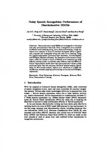
2. SYSTEM ARCHITECTURE FOR HIGH FRAME RATE OPERATION Fig. 1 shows overall algorithm flow of the proposed multi-object recognition. It consists of 3 stages: visual perception, parallel processing, and object decision. The visual perception stage preliminary extracts static features such as intensity, color and orientation, and dynamic feature such as motion vector from the input image to generate saliency map. Then, based on this map, it determines region-of-interests (ROIs) for each object in a unit of 40x40 pixel sized tile, called grid-tile. After that, the parallel processing stage extracts feature points out of the selected ROI gridtiles using parallel and repetitive kernel processing, and generates descriptor vectors. Lastly, the final object decision is made by iterative database matching for descriptor vectors of each object. This grid-based ROI processing, which divides an input image into over a number of small sized grid-tiles and processes the ROIs of objects based on them, enables fine-grained boundary extraction for
SW Algorithm Input Image
dynamic feature
1. Visual Perception
Motion
Grid-based ROI Processing Input image
Seed points
static features
Intensity Color Orientation
Saliency map Object ROI detection
Saliency based ROI detection Region-of-Interests (ROI) Task 20
Visual Image Processing
2. Parallel Processing
38
20
Key-Point Extraction
78/192 grid-tiles
Descriptor Vector Generation
Descriptor Vectors / Obj. Nearest Database Matching
3. Object Decision
Voting Scheme Final Recognition
Cup
Cigar Box
Teddy Bear
(a) Block Diagram
Iterative database matching Recognition Results / Obj.
Fig. 1 3-Stage Multi-Object Recognition Algorithm each object and results in workload reduction of input image. By applying this model to the 164 sample images of multi-object database Berkeley Segmentation Database (BSD300) [6], object ROIs of images are measured to 41% of overall area on average. This means the workloads of the following parallel processing and object decision stage can be also reduced in similar portion by processing only the selected region. As a result, workload reduction in algorithm level greatly improves energy efficiency in recognition processing by eliminating needless processing for uninterested area of the image, originally supposed to be processed. Fig. 2 (a) shows the block diagram of the proposed recognition processor consisting of 21 IP blocks. The neural perception engine (NPE) is responsible for the visual perception stage. It extracts various features from the input image and generates ROIs for each object in a grid-tile unit. 16 SIMD processor units (SPU) are responsible for the parallel processing stage. They have 4 separated power domains and generate descriptor vectors for the selected ROIs. A decision processor (DP) performs the object decision stage with dedicated blocks for vector distance calculation and matching. A SPU task/power manager (STM) is specially devised to distribute ROI grid-tile tasks from the NPE to the 16 SPUs and to manage 4 power domains of the 16 SPUs. 2 memory interfaces are integrated to communicate with 2 external memories. To increase the parallelism and utilization of the proposed hardware, the proposed 3 object recognition stages, the visual attention, parallel processing, and object decision are executed in the pipeline as shown in Fig. 2 (b). Pipelined data are ROI grid-tile tasks and descriptor vectors for between the 1st and 2nd stage and the 2nd and 3rd stage, respectively. For efficient task pipelining, the execution times of 3 stages are controlled to be balanced. The execution time of visual perception is deterministic because it is mainly composed of repeated feature extractions and normalizations. Meanwhile, the execution times of parallel processing and object decision stage are varied according to their workloads, the number of extracted ROI grid-tiles and descriptor vectors, respectively. Therefore, to balance the execution times of 3 stages, the STM controls the execution time of the parallel processing and object decision to the one of visual perception, which is fitted to target pipeline time 16ms. To control
(b) 3-Stage Task Pipelining Fig. 2 System Architecture the execution time of the parallel processing stage, the STM performs workload-aware task scheduling. It determines the number of the operating SPUs according to the amount of measured ROI grid-tiles. Since the number of processing units increases in proportional to the workload, the execution time is kept in constant level. And the execution time is controlled by performing scheduling more aggressively or conservatively. The execution time of object decision stage is controlled by adjusting the size of applied database in vector matching process. Based on the vector matching algorithm of [7], the overall execution time of the object decision stage is estimated with the number of input descriptor vectors and the size of applied database. Using this, the execution time can be controlled by configuring database coverage rate of the DP after measuring the number of descriptor vectors from the parallel processing stage. As a result, the execution time of the 2nd and 3rd stage is balanced to 16ms, even under varying workload conditions, and the overall processor achieves 60 fps frame rate.
3. DYNAMIC POWER MANAGEMENT In this chapter, we will discuss about the dynamic power management schemes applied to the proposed processor. Fig. 3 shows overall power management architecture. First of all,
(a) Parameters
3.1 POWER DOMAIN SEPARATION OVERHEAD Power gating is an efficient and robust way to reduce leakage power in deep sub-micron technology by disconnecting idle blocks from the power supply [8]. To avoid excessive design overheads of on-chip power gating, such as header and footer transistor addition to logic and memory blocks and gate signal generation, off-chip power gating is adopted with a simple backend process using standard library. For off-chip power gating, all we have to do in design time is to separate the power domain of chip into several pieces and generate request signals for power gating to external regulators. Therefore, major overheads of off-chip power gating are summarized as two things: area overhead in on-chip domain and additional regulators in off-chip domain. Fig. 4 (a) shows the additional spaces around the processing core required for power domain separation, which are mainly for power rings. In this figure, the additional length for domain separation is denoted as x where the width and height of the SPU core is defined as a and b, respectively. The x is a summated value that includes all required factors such as power ring space, interval distance, and margin. The number of separated power domains is N, while the number of the clustered SPU cores in same power domain is M. It is assumed that the number of SPU cores in each power domain is even. Therefore, NxM should be equal to the total number of the SPUs, or 16 in this design. It is also assumed that the ratio of the core area is kept even if the M is not the square of integer. With these configurations, the total area of N separated power domains with NxM SPUs is as following.
area overhead ratio (%)
# of additional ext. regulators
Fig. 3 Power Management Architecture regulators for power supply of the processor exist in external and ground rails of off-chip and on-chip are all shared. In the chip, the NPE, DP, and STM are always on domain, while the 16 SPUs are in externally controlled 4 separated power domains. The STM is responsible for managing the 4 power domains of the 16 SPUs according to the workload variations of the NPE. In this power domain architecture, we will discuss following 3 issues for low power consumption of the processor. First, the overhead of power domain separation is analyzed according to the number of power domains. Second, workload-aware scheduling scheme is proposed for efficient power gating and its power reduction effect is evaluated. Third, fine-grained clock gating scheme is explained for further reduction of operating power in activated domains.
(b) Overheads Fig. 4. Power domain separation Total area: ( M ⋅a + 2⋅ x)×( M ⋅b + 2⋅ x)× N The area overhead of domain separation is computed as follows.
Overhead: ( M ⋅a + 2⋅ x)×( M ⋅b + 2⋅ x)× N − M ⋅ N ⋅a⋅b = 2 ⋅ N ⋅( M ⋅( a + b)⋅ x + 2 ⋅ x 2 )
Since the total number of SPU cores is 16, the number of separated power domains N can be configured to 1, 2, 4, 8, and 16, while the number of clustered SPU cores is 16, 8, 4, 2, and 1, respectively. The following equation shows the overhead ratio defined as the ratio of the area overhead and the core area.
Ratio =
x2 2 ⋅ N ⋅( M ⋅ ( a + b ) ⋅ x + 2 ⋅ x 2 ) ( a + b ) ⋅ x = ⋅ N+ ⋅N 2 ⋅ a ⋅b 4 ⋅ a ⋅b N ⋅ M ⋅ a ⋅b
Meanwhile, the number of additional regulators with enable is the same with the number of separated power domains N. External overhead = N (regulator devices) The graph of Fig. 4 (b) shows the internal and external overhead of power domain separation. For this, the values of a, b, and x are defined to 1.0mm, 1.7mm, and 0.04mm, respectively, which are measured from real physical implementation in a 0.13μm process.
3.2 WORKLOAD-AWARE TASK SCHEDULING To perform power gating under the condition that the power domain of the 16 SPUs is separated into N domains, an appropriate scheduling scheme is demanded. To this end, the SPU task/power manager (STM) performs workload-aware task scheduling (WATS) when it distributes ROI grid-tile tasks to the 16 SPUs. Fig. 5 shows the flow chart of the WATS. First, the STM measures the workload of the current frame based on the number of extracted ROI grid-tiles.
Input image
Measure workload
x: # of ROI grid-tiles
How many levels (N) ? Light
x