We have constructed a voltage adder [9] to implement some dendritic computations, and have simulated this circuit using carbon nanotube SPICE models.
A Carbon Nanotube Implementation of Temporal and Spatial Dendritic Computations Alice C. Parker, Jonathan Joshi, Chih-Chieh Hsu and Nav Aman Deep Singh Department of Electrical Engineering University of Southern California Abstract—A neural dendritic computational circuit design is presented here. The circuit models the result of action potentials applied to biological synapses on a portion of a dendritic tree. The resultant excitatory post synaptic potentials (EPSPs) are combined in a dendritic tree that demonstrates linear, superlinear and sublinear summation of both spatially and temporally separated EPSPs. The synapse circuit models include neurotransmitter action, reuptake and membrane potentials. The output of the circuit is a combined Excitatory Post Synaptic Potential (EPSP). The circuit is simulated using carbon nanotube SPICE models. Variations of this design can be implemented to create a variety of dendritic computational subunits.
I. I NTRODUCTION Within the neurons in the cortex, significant dendritic computations occur that affect the probability and frequency of neural firing. Action potentials arriving at the synapses create post-synaptic potentials on the dendritic arbor that combine in complex ways (e.g. [1], [2], [3]). There is growing consensus among neuroscientists that aspects of dendritic behavior contribute significantly to cortical functioning. The biological synapse is complex, with controllable transmitters that can decrease or increase the excitability of the postsynaptic receptors. The activation probability of a given synaptic junction is regulated by the amount and timing of presynaptic and postsynaptic activity. Neurotransmitters must be present in sufficient amounts to develop post-synaptic potentials (PSPs), and the concentration of transmitters released can affect the height and duration of the PSP [4]. A second area of complexity is the ion channel, modeled biomimetically, e.g. by Hasler [5]. Ion channel conductance in turn affects membrane potential. Action potentials impinging on the synaptic cleft could result in temporal summation of the resulting PSPs, increasing the likelihood of the post-synaptic neuron eventually firing. A third area of complexity involves the dendritic computations that occur on the EPSPs [6] [2]. These computations include linear, sublinear and superlinear additions whereas modeling inhibitory inputs is the subject of a future paper. Carbon nanotubes may support the scale and interconnection density of a synthetic cortex. They are extremely small (a few nm. in diameter), current flow is largely ballistic (like the flow of electrons in free space), capacitances are in attofarads, Support for this research has been provided by the Viterbi School of Engineering at the University of Southern California and NSF Grant 0726815
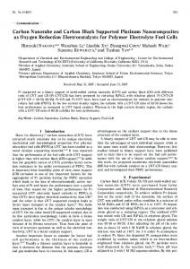
and rise and fall times in picoseconds. Appropriate interfaces can convert to biological signal levels and delays. Channel resistance is primarily due to the quantum resistance at the junction between the nanotubes and metallic connections, creating a challenge for analog circuit design. Carbon nanotubes have been shown to form dendritic structures, which may facilitate their use in synthetic neurons [7]. Finally, nanotubes have been shown to induce minimum immune system reactions in living tissue, making prosthetic devices with carbon nanotubes desirable [8]. We designed and simulated a carbon nanotube transistor circuit model of a neural synapse that captures, in a coarse manner, the actions of neurotransmitters, ion channel mechanisms, and temporal summation of PSPs. We have focused on excitatory PSPs (EPSPs) first, and have chosen economy of size over exact replication of waveforms, to facilitate scaling to cortical-sized biomimetic structures. We have constructed a voltage adder [9] to implement some dendritic computations, and have simulated this circuit using carbon nanotube SPICE models. This adder is tunable to support sublinear to superlinear summations of PSPs. We have constructed a small portion of a dendritic arbor, and shown how action potentials impinging on the presynaptic terminals of the arbor produce output PSPs that are a function of the EPSPs invoked at each synapse of the arbor. II. BACKGROUND Many electronic neurons have biomimetic features (e.g. [10]). The most notable research includes Mead’s artificial retina [11]. This significant work originated with Mahowald and Mead [12], followed by Boahen [13] [14] and more recently Hasler [5]. Hynna and Boahen report on a circuit that generates a calcium spike with attention paid to exact replication of waveforms, and describe incorporation of the calcium spike circuit in an entire neuron circuit [15]. Some mixed-signal electronic models close to biological neurons include Liu and Frenzel’s spike train neuron, with a 10transistor mixed-signal synapse [16], and Pan’s bipolar neuron [17]. An 8-transistor CMOS synapse [18] is close in scale and nature to our synapse, although they plan to use the synapse for summation of inputs from many pre-synaptic sites. Analog synapses have been reported by Pinto et al. [19] and Lee et al. [20] and a phase-lock loop synapse has been reported by Volkovskii [21]. The strength of our model and similar models is the correspondence between individual circuit elements and
specific physiological mechanisms in the biological neuron that allows us to vary synapse behavior easily with control inputs. This, and our choice of carbon nanotube technology, differentiates this work. Elias modeled dendritic computations as early as 1992 [22]. Hasler and Farquhar also model dendritic transmission [5], [10], as do others (e.g. Arthur [23] and Rasche [24]). Existing cable models could be integrated with our computations for a complete dendritic model. Single-walled carbon nanotubes avoid most of the fundamental scaling limitations of silicon, making them suitable for a synthetic cortex [25]. Liu, Han and Zhou have demonstrated directional growth of high-density single-walled carbon nanotubes on a- and r-plane sapphire substrates over large areas [26]. This technique may enable registration-free fabrication of nanotube devices and lead to integrable and scalable nanotube systems, including synthetic cortex circuits. They have developed a novel nanotube-on-insulator (NOI) approach, and a way to transfer these nanotube arrays to flexible substrates. Efforts have been made in recent years on modeling CNFETs [27] [28] and CNT interconnects [29] [30], to evaluate the potential performance at the device level. Most of the reported models to date used a single lumped gate capacitance and ideal ballistic model to evaluate the dynamic performance [31] [32]. To evaluate CNFET circuit performance with improved accuracy, a CNFET device model with a more complete circuit-compatible structure and including the typical device non-idealities was constructed [33]. This recent publication presents a novel circuit-compatible compact SPICE model for short channel length (5nm 100nm), quasi-ballistic single wall carbon nanotube field-effect transistors (CNFETs). III. T HE C ARBON NANOTUBE S YNAPTIC C IRCUIT The carbon nanotube synaptic circuit [34] [35] is shown in Figure 1. Action potentials (see Figure 2) arrive from the presynaptic neuron and terminate in our synaptic circuit. The simple action potential used here is an approximation of a typical biological action potential [36]. An incoming action potential will cause the potential in the synaptic cleft to rise. The PFET limits the peak amplitude of the synaptic cleft potential by turning off before the synaptic cleft potential rises to Vdd. The synaptic cleft potential in the electronic neuron (Figure 1) models the biological release of neurotransmitters stored in the presynaptic neuron into the cleft, where they bind to receptor proteins on the recipient (postsynaptic) neuron, causing the potential across the postsynaptic neural membrane to change. Once the neurotransmitters are released from the presynaptic terminal and bound in the postsynaptic terminal, they will be cleared from the synaptic cleft for reuse by reuptake mechanisms modeled via the pull-down network attached to the synaptic cleft [4].1 The re-uptake control 1 Since the SPICE model used in this study is geared toward short gate length transistors with near-ballistic transport, we use three transistors in series to model the resistance that represents the reuptake delay. The quantum contact resistances of the three transistors are added in series.
Fig. 1.
The Carbon Nanotube Synaptic Circuit
Fig. 2. The Action Potential and PSP at the Dendritic Trunk under Normal Operation
voltage, R allows the efficiency of the reuptake mechanism to be tuned. The action potential is inverted and used to block pull down of the synaptic cleft potential to delay reuptake of the neurotransmitter at the presynaptic neuron while there is a positive action potential. Reuptake can be inhibited or slowed by lowering the reuptake control voltage R. The increase in potential in the synaptic cleft will temporarily turn on the transistor connected to the ion electromotive force control, E Channel, causing the potential at Synaptic Interior to rise. This models the change in biological membrane potential due to the increased conductance of neurotransmitter gated ion channels and the subsequent influx of charge carrying ions (e.g. sodium). A tunable pull-down network 2 controls the cell interior’s return to resting potential (steady state). The synaptic interior potential is transferred through a resistive connection to the dendritic trunk, which carries the postsynaptic potential (PSP) to the neuron cell body. The weight control allows the importance of this synapse to be tuned with learning. The dendrite trunk terminates on the gate of a single test load NFET that is removed when the synapse is connected to other neural components. In the archetypical biological neuron we are modeling, potentials range from around -75mV to +40mV with action potentials peaking around +40mV. Since the carbon nanotube synapse is designed to operate with Vdd around 0.9V and with 0.0V (Ground) as the resting potential, the potentials were scaled accordingly, with 0V circuit potential corresponding to -75mV biological potential and 0.9V circuit potential corre2 Three
transistors in series provides the Rpulldown resistance.
adder_cnt
Vdd
900m AP1, AP2, AP3, and AP4
800m gnd
gnd
gnd
gnd
700m V2
V1
Vout
600m Voltages (lin)
gnd
500m Summation of PSP1, PSP2, PSP3, and PSP4 400m 300m
Vss
200m PSP1, PSP2, PSP3, and PSP4 100m 0
Fig. 3.
0
The Voltage Adder
20p
40p 60p Time (lin) (TIME)
80p
100p
Fig. 5. The Summation of Four EPSPs in the Dendritic Arbor: AP indicates Action Potential
adder_cnt
900m 800m
AP1
AP2
PSP1
PSP2
700m
Fig. 4.
The Dendritic Arbor Portion
Voltages (lin)
600m 500m 400m 300m 200m
sponding to 40mV biological potential. Likewise, the speed of the carbon nanotubes allowed us to scale the delays with about 1 ms in the biological neuron scaling to about 2 ps in the nanotube neuron [36]. IV. T HE VOLTAGE A DDER AND D ENDRITIC A RBOR The adder circuit [9] is shown in Figure 3. A block diagram of the dendritic arbor portion is shown in Figure 4. There are four synapses in the arbor, each on a separate dendritic branch. V. E XPERIMENTS WITH THE D ENDRITIC A RBOR C IRCUIT We performed several experiments with the dendritic arbor circuit. First, we simulated four synapses in the dendritic arbor excited with action potentials arriving at the same time, with linear addition. Then we simulated the addition of two synapses with action potentials arriving at varying times. For the third phase of the simulations, we varied the additions to be sublinear and superlinear. Finally we simulated the dendritic arbor with some PSPs weakened as a result of reduced neurotransmitter concentration (modeled by decreasing the source voltage on the PMOS pull up transistor in the synapse). The postsynaptic potential appearing at the dendritic trunk is shown in Figure 2. This potential is approximately 14% of the action potential and the duration is about 6 times as long as the action potential, similar to EPSPs described in the literature. In the first experiment, we tuned the dendritic PSP adders by adjusting transistor sizes to be linear, and all four synapses
PSP1 + PSP2 linearly
100m 0 0
20p
40p 60p Time (lin) (TIME)
80p
100p
Fig. 6. The Temporal and Spatial Summation of Two EPSPs Excited by Action Potentials Arriving at Different Times
were excited simultaneously, as shown in Figure 5. In the second experiment, we simulated two action potentials (APs) arriving at staggered times so that the two EPSPs peaked at different times, demonstrating temporal and spatial summation. The resultant total EPSP is shown in Figure 6. A third experiment shows the types of PSP computation possible using our circuitry: superlinear, sublinear and linear, shown in Figure 7. The final experiment (Figure 8) illustrates the summation of weak and strong EPSPs. VI. C ONCLUSIONS A typical carbon nanotube synapse has been designed and simulated using SPICE. This synapse has been replicated and used in a portion of a dendritic arbor to illustrate some varieties of dendritic computations that occur. The dendritic computation shown is one of several types of computations that occur. ACKNOWLEDGMENT The authors acknowledge helpful suggestions of Lanre Ayo, Bartlett Mel, Jie Deng, Philip Wong and Norberto Grzywacz.
adder_cnt2
900m AP1 and AP2 800m 700m
Voltages (lin)
600m 500m 400m
PSP1 + PSP2 superlinearly PSP1 + PSP2 linearly
300m
PSP1 + PSP2 sublinearly 200m 100m
PSP1 and PSP2
0 0
Fig. 7.
20p
40p 60p Time (lin) (TIME)
80p
100p
EPSPs Summed Linearly, Sublinearly, and Superlinearly
adder_cnt
900m
AP1 and AP2
800m 700m
Voltages (lin)
600m 500m 400m 300m 200m PSP1 + PSP2 100m
PSP1 (strong)
0
PSP2 (weak)
0
Fig. 8.
20p
40p 60p Time (lin) (TIME)
80p
100p
Summation of Weak and Strong EPSPs
R EFERENCES [1] Mel, B. W., “Synaptic Integration In an Excitable Dendritic Tree”, J. Neurophysiol. 70, pp. 1086-1101, 1993. [2] Polsky, A., Mel, B. W., and Schiller, J., “Computational subunits in thin dendrites of pyramidal cells”.Nature Neuroscience,V. 7, pp. 621627, 2004. [3] Koch, C, and Segev, I., “The Role of Single Neurons in Information Processing”, Nature Neuroscience Supplement, V. 3, Nov., 2000. [4] Shepherd, G. “Introduction to Synaptic Circuits,” in The Synaptic Organization of the Brain, edited by Gordon Shepherd, 5th edition, Oxford University Press, 2004. [5] Hasler, P., Farquhar, E., and Gordon, C., “Building Large Networks of Biological Neurons”, Engr. in Medicine and Biology Conference, 2006. [6] Mel, B., and Schiller, J., “On the Fight Between Excitation and Inhibition: Location is Everything”, Science’s STKE, 2004. [7] Cao, A., et al., “Carbon nanotube dendrites: availability and their growth model”, Materials Research Bulletin, Volume 36, Issues 13-14, 1 November 2001, Pages 2519-2523. [8] Bianco, A., et al., “Biomedical applications of functionalised carbon nanotubes”, Chem. Commun., 2005, pp. 571 - 577. [9] Chaoui, H., “CMOS Analogue Adder”, Electronics Letters, V. 31, No. 3, Feb., 1995, pp. 180-181. [10] Farquhar, E., and Hasler, P., “ Bio-Physically Inspired Silicon Neuron,”IEEE Trans. on Circuits and Systems, Vol. 52, No. 3, March 2005, pp. 477-488. [11] Mead, C, Analog VLSI and Neural Systems, 1989, Addison-Wesley Longman, Boston. [12] Mahowald, M., VLSI analogs of neuronal visual processing: a synthesis
of form and function, Ph.D. dissertation, California Institute of Technology, Pasadena, 1992. [13] Boahen, K., “Neuromorphic microchips,” Scientific American, May, 2005, pp. 56-63. [14] Zaghloul, K.A.; Boahen, K., ”Optic nerve signals in a neuromorphic chip II: testing and results,” Biomedical Engineering, IEEE Transactions on , vol.51, no.4, pp. 667- 675, April 2004. [15] Hynna, K.M.; Boahen, K., ”Neuronal ion-channel dynamics in silicon,” Circuits and Systems, 2006. ISCAS 2006.Proceedings. 2006 IEEE International Symposium on, pp. 21-24 May 2006 [16] Liu, B., and Frenzel, J.F., “A CMOS neuron for VLSI implementation of pulsed neural networks,”Proc. 28th Ann. Conf. Ind. Electron. IECON02, Nov. 5-8, Sevilla, Spain, pp. 3182-3185, 2002. [17] Pan, D. and Wilamowski, B.M., ”A VLSI implementation of mixedsignal mode bipolar neuron circuitry,” IJCNN, vol.2, pp. 971- 976 vol.2, 20-24 July 2003 [18] Shi, R. Z. and Horiuchi, T., “A Summating, Exponentially-Decaying CMOS Synapse for Spiking Neural Systems,” Neural Information Processing Systems Foundation NIPS 2003. [19] Pinto, R. D, et al., ”Synchronous behavior of two coupled electronic neurons,” Phys Rev E., vol. 62, pp. 2644-56, 2000. [20] Lee, Y., Lee, J., Kim, Y., and Ayers, J., “A Low Power CMOS Adaptive Electronic Central Pattern Generator Design,” 48th Midwest Symposium on Circuits and Systems, 7-10 Aug. 2005 page(s): 1350- 1353 Vol. 2. [21] Volkovskii, A., et al., “Analog electronic model of the lobster pyloric central pattern generator,” Institute of Physics Publishing Journal of Physics: Conference Series 23 (2005) 4757 doi:10.1088/17426596/23/1/005 International Conference on Control and Synchronzation of Dynamical Systems [22] Elias, J.G., Chu, H-H, and Meshreki, S.M., “Silicon implementation of an artificial dendritic tree,”IJCNN, 1992, Volume 1, pp. 154-159. [23] Arthur, J. and Boahen, K., “Recurrently Connected Silicon Neurons with Active Dendrites for One-Shot Learning”, Proceedings, 2004 IEEE International Joint Conference on Neural Networks, July 2004, Volume: 3, page(s): 1699- 1704. [24] Rasche, C., and Douglas, R., “Forward and Backpropagation in a Silicon Dendrite”, IEEE Transactions on Neural Networks, Vol. 12, No. 2, March, 2001, pp.386-393. [25] Parker, A. C., Friesz, A. K., Pakdaman, A., “Towards a Nanoscale Artificial Cortex,” Proceedings of The 2006 International Conference on Computing in Nanotechnology (CNAN’06): June 26-29, 2006. [26] Liu, X., Han, S., and Zhou, C. “A Novel Nanotube-on-Insulator (NOI) Approach toward Nanotube Devices”,Nano Letters, 6, 34-39 (2006). [27] K. Natori, Y. Kimura, and T. Shimizu, ”Characteristics of a carbon nanotube field-effect transistor analyzed as a ballistic nanowire field-effect transistor,” J. of Applied Physics, vol. 97, pp. 034306, 2005. [28] Guo, J., Lundstrom, M., and Datta, S.. ”Performance projections for ballistic carbon nanotube field-effect transistors,” Applied Physics Letters, vol. 80, pp. 3192-3194, 2002. [29] Burke, P., ”Carbon nanotube devices for GHz to THz applications”, 2003. [30] Naeemi, A., Sarvari, R., and Meindl, J. D., ”Performance comparison between carbon nanotube and copper interconnects for gigascale integration (GSI),” Electron Dev. Let., IEEE, vol. 26, pp. 84-86, 2005. [31] Raychowdhury, A., Mukhopadhyay, S., and Roy, K., ”A circuitcompatible model of ballistic carbon nanotube field-effect transistors,” Computer-Aided Design of Integrated Circuits and Systems, IEEE Transactions on, vol. 23, pp. 1411-1420, 2004. [32] Dwyer, C., Cheung, M., and Sorin, D., ”Semi-empirical SPICE models for carbon nanotube FET logic,” 2004. [33] Deng, J., and Wong, H.-S. P., “A Circuit-Compatible SPICE model for Enhancement Mode Carbon Nanotube Field Effect Transistors,” Conference on Simulation of Semiconductor Devices and Processes, SISPAD 2006, Monterey, CA, Sept. 6 8, pp. 166 169, 2006. [34] Parker, A. C., Friesz, A. K., and Tseng, K-C, “Biomimetic Cortical Nanocircuits”, in Bio-inspired and Nano-scale Integrated Computing, editor M. Eshaghian-Wilner, Wiley, Inc., to be published 2008. [35] Friesz, A. F., and Parker, A. C., “A Biomimetic Carbon Nanotube Synapse”, Poster Presentation, Biomedical Engineering Conference, 2007, [36] Chang,Y-M, Rosene, D. L., Killiany, R. J., Mangiamele, L. A. and Luebke, J. I., “Increased Action Potential Firing Rates of Layer 2/3 Pyramidal Cells in the Prefrontal Cortex are Significantly Related to Cognitive Performance in Aged Monkeys”, Cerebral Cortex 2005 15(4):409-418 Oxford University Press.