A Complete Multi-Processor System-on-Chip FPGA-Based Emulation Framework
†
Pablo G. Del Valle? , David Atienza†? , Ivan Magan? , Javier G. Flores? , Esther A. Perez? , Jose M. Mendias? , Luca Benini‡ , Giovanni De Micheli† ? DACYA/UCM, Juan del Rosal 8, 28040 Madrid, Spain.
[email protected], {datienza, mendias}@dacya.ucm.es LSI/EPFL, EPFL-IC-ISIM-LSI Station 14, 1015 Lausanne, Switzerland. {david.atienza, giovanni.demicheli}@epfl.ch ‡ DEIS/Bologna, Viale Risorgimento 2, 40136 Bologna, Italy. {lbenini}@deis.unibo.it
Abstract— With the growing complexity in consumer embedded products and the improvements in process technology, Multi-Processor System-On-Chip (MPSoC) architectures have become widespread. These new systems are very complex to design as they must execute multiple complex real-time applications (e.g. video processing, or videogames), while meeting several additional design constraints (e.g. energy consumption or time-to-market). Therefore, mechanisms to efficiently explore the different possible HW-SW design interactions in complete MPSoC systems are in great need. In this paper, we present a new FPGA-based emulation framework that allows designers to rapidly explore a large range of MPSoC design alternatives at the cycle-accurate level. Our results show that the proposed framework is able to extract a number of critical statistics from processing cores, memory and interconnection systems, with a speed-up of three orders of magnitude compared to cycleaccurate MPSoC simulators.
I. I NTRODUCTION New applications ported to embedded systems (e.g. scalable video rendering or multi-band wireless protocols) demand complex singlechip multi-processor designs to meet their real-time processing requirements while respecting other critical embedded design constraints, such as low energy consumption or reduced implementation size. Furthermore, the consumer market is reducing more and more the time-to-market and price [15]. Thus, not making feasible any longer complete redesigns of such multi-core systems from scratch. In this context, Multi-Processor Systems-on-Chips (MPSoC) have been proposed as a promising solution for all these previous problems, since they are single-chip architectures consisting of complex integrated components communicating with each other at very high speeds [15]. Nevertheless, one of their main design challenges is the fast exploration of multiple hardware (HW) and software (SW) implementation alternatives with accurate estimations of performance, energy and power to tune the MPSoC architecture in an early stage of the design process. Several MPSoC simulators have been proposed, both at transaction and cycle-accurate levels using HDL languages and SystemC. Although they achieve accurate estimations, they are limited in performance (circa 10-100 Khz) due to signal management overhead. Thus, such environments cannot be used to analyze MPSoC solutions with complex embedded applications and large inputs to cover the variations in data loads at run-time. Moreover, higher abstraction levels simulators attain faster simulation speeds, but at the cost of a significant loss of accuracy. Hence, they are not suitable for finegrained architectural tuning. One solution for the speed problems of cycle-accurate simulators is HW emulation. Various MPSoC emulation frameworks have been proposed [20], [9], [1]. However, they are usually very expensive for embedded design (between $100K and $1M). Moreover, they are not flexible enough for MPSoC architecture exploration since they mainly aim at large MPSoCs prototyping or SW debugging. Typically, the
3-901882-19-7 2006 IFIP
140
baseline architectures (e.g. processing cores or interconnections) are proprietary, not permitting internal changes. In this paper, we present a new FPGA-based emulation framework that allows to explore a large range of design alternatives of complete MPSoC systems at the cycle-accurate level. Its modular architecture can extract a large range of critical statistics from three key architectural levels of MPSoC systems (i.e. processing cores, memory subsystem and interconnection mechanisms), while real-life applications are executed. Our experiments show that this framework achieves detailed cycle-accurate reports of these three levels with a speed-up of three orders of magnitude compared to state-of-the-art cycle-accurate MPSoC simulators. The remainder of the paper is organized as follows. In Section II, we summarize related work of MPSoC analysis and testing. In Section III, we present the flexible architecture of the MPSoC emulation platform and the statistics extraction mechanism. In Section IV, we present the advanced mechanism incorporated to decouple the emulation performed from the physical characteristics of the present hardware. In Section V, we detail how the HW/SW emulation process of MPSoC architectures is performed. In Section VI, we illustrate the speed and versatility of our emulation framework for MPSoC design. Finally, in Section VII, we draw our conclusions. II. R ELATED W ORK It is widely accepted that MPSoCs represent a promising solution for forthcoming complex embedded systems [15]. This has spurred research on modelling and prototyping MPSoC designs, both using HW and SW. From the SW viewpoint, different solutions have been suggested at different abstraction levels, enabling tradeoffs between simulation speed and accuracy. First, fast analytical models have been proposed to prune very distinct design options using high level languages (e.g. C or C++) [17], [5]. Second, transaction-level modelling in SystemC, both at the academic [18], [21] and industrial level [16], [6], have enabled more accuracy in system-level simulation at the cost of sacrificing simulation speed (circa 100-200 Khz). Thus, not enabling extensive testing with large and various systems due to the too long simulation times, conversely to our emulation framework. Moreover, in most of the cases, they are only limited to a range of propietary interfaces (e.g. AMBA or LISA). Finally, important research has been done to obtain cycle-accurate frameworks in SystemC or HDL languages. In this context, companies have developed cycle-accurate simulators using post-synthesis libraries from HW vendors [12], [19]. However, their simulation speeds (10 to 50 Khz) are unsuitable for complex MPSoC exploration and validation. In the academic context, the MPARM SystemC framework presented in [3] is one of the most complete simulators for system-exploration since it includes cycle-accurate cores, complex memory hierarchies (e.g.
caches, scratchpads) and interconnection mechanisms (e.g. AMBA or STBus). It can extract reliable energy and performance figures, but its major shortcoming is its simulation speed (120 Khz in a Pentium IV at 2.8 Ghz, see Section VI for further details). From the HW viewpoint, an important alternative for MPSoC prototyping and validation is HW emulation. In industry, one of the most complete sets of statistics is provided by Palladium II [20], which can accomodate very complex systems (i.e. up to 256 Mgate). However, its main disadvantages are its operation frequency (circa 1.6 Mhz) and cost (around $1 million). Then, ASIC Integrator [2] is much faster for MPSoC architectural exploration. However, its major drawback is the limitation to up to five ARM-based cores and only AMBA interconnection mechanisms. The same limitation of proprietary cores usage for exploration occurs with Heron [9]. Finally, other relevant industrial emulation approaches are System Explore [1] and Zebu-XL [8], both based in multi-FPGA emulation in the order of Mhz. They can be used to validate IPs, but are not flexible enough for fast MPSoC design exploration or detailed statistics extraction. In the academic world, the most complete emulation platform up-to-date for exploring MPSoC alternatives is TC4SOC [7]. It uses a propietary 32-bit VLIW core and enables the exploration of the interconnection mechanisms and different protocols by using an FPGA to reconfigure the network interfaces. Also, [4] proposes a HW/SW emulation framework that enables the exploration of different Network-onChip (NoC) interconnection mechanisms. However, they do not allow designers to exhaustively extract statistics and explore the other two architectural levels we propose, namely memory hierarchy and processing cores. III. MPS O C E MULATION A RCHITECTURE The proposed MPSoC framework uses FPGA emulation as the key element to introduce SW to real HW, execute that SW on the considered MPSoC platform capable of multi-megahertz speeds, and extract detailed system statistics. An overview of the baseline HW architecture of our MPSoC emulation platform is depicted in Figure 1. It consists of four main elements from where designers can get critical statistics about MPSoC designs: 1) The evaluation (e.g. performance, generated traffic or locality of references) of different MPSoC processing cores, such as, Power PC, ARM or VLIW cores. 2) The definition of the first level of the on-chip memory hierarchy (i.e. I-cache, D-cache and scratchpad memories), as well as main memories, namely private and shared memories between processors. 3) The evaluation of different interconnection mechanisms between the first level of the memory hierarchy and the main memory (i.e. buses and NoC interconnections). 4) The obtained statistics are automatically sent to a host PC via an standard Ethernet connection thanks to our own developed statistics extraction subsystem. It includes a graphical interface running onto the host PC to analyze the information received and provide detailed reports. These elements are designed in standard and parameterizable VHDL and mapped onto a Xilinx Virtex 2 Pro vp30 board (or V2VP30) with 3M gates, which costs $2000 approximately in the market, and that includes two embedded Power PCs, various types of memories (i.e. SRAM, SDRAM and DDR) and an Ethernet port. However, any other FPGA could be used instead. The only requirements are the availability of an Ethernet core to download the statistics, a compiler for the included cores and a method to upload both the FPGA synthesis of our framework and the compiled code of
141
Fig. 1.
Overview of the HW architecture of the emulated MPSoC
the application under study. In our case, Xilinx provides all these tools in its Embedded Development Kit (EDK) framework for FPGAs. In addition, remark that the purpose of our emulator is not the prototyping of final HW components in MPSoC systems, but the emulation and fast exploration for designers of desired characteristics of the eventual system. Therefore, our framework includes mechanisms to configure the exploration and hide the physical characteristics of the underlying HW that do not match the selected values, conversely to traditional prototyping. A detailed explanation of the included mechanisms is given in Section IV. In the following subsections we describe in detail the architecture and advanced emulation mechanisms of the different elements included in our emulation platform. Also, it is outlined the synthesis figures for each component. A. Processing Elements In our framework, any type of processor or coprocessor core can be included, both propietary and public ones. The accepted input forms are netlist mapping onto the underlying FPGA and HDL languages (i.e. Verilog, VHDL or Synthesizable SystemC). This addition of cores is possible since the memory controller that receives the memory requests in our system includes an external pinout interface and protocol that can be easily modified to match the respective ones of the studied processor (see Subsection III-B). Moreover, only the instruction set processing part of the core is required because its memory hierarchy (e.g. caches or scratchpad) are replaced by our framework to explore different memory configurations. In the current version of the system, we have ported a hard-core (PowerPC 405) and a soft-core (Microblaze) provided by Xilinx. None includes HDL sources, only netlist mapping, and the inclusion process for their pinout interfaces and protocols required one week. Regarding platform’s scalability, it is worth to mention that a complete Microblaze requires only 4% of the total resources of our V2VP30 FPGA (574 out of 13.696 slices). B. Memory Hierarchy As Figure 1 indicates, in the basic emulated architecture two memory levels presently exist: L1 cache memories and main memories. However, it is a matter of minutes to add additional cache memory levels or private memories to each processing element, either on a processor basis or by processor groups. The main element
in the memory hierarchy that enables this easy integration of new memory devices and protocols is the memory controller. One memory controller is connected to each processing core to capture all memory requests of the respective processors. Then, it forwards them to the necessary element of the memory subsystem according to the demanded memory address. In the current implementation, it takes 2% of the total available resources of our V2VP30 FPGA (270 of 13.696 slices), and includes interfaces and protocols for four memory components and three different memory address ranges: 1) Private scratchpad memory, addressable by SW at a configurable memory position and with unrestricted size, as long as enough RAM resources exist. It also allows configuring latency and can be used to place instructions or data. Its synthesis takes 1% of the V2VP30 (181 of 13.696 slices), apart from used RAM resources. 2) Private main memory, cacheable or non-cacheable, addressable in a configurable memory range of each processor. It is also possible to configure its size and latency. Its synthesis takes an insignificant amount of the total V2VP30 FPGA resources (apart again from the used RAM). 3) Shared main memory, cacheable or non-cacheable according to user’s configuration. It is possible to configure its size and latency. Its inclusion does not take any part in the FPGA since it uses real memories (i.e. SRAM, SDRAM or DDR) available on the board. 4) Private HW-controlled data and instruction caches, transparent to the processors, and embedded before the cacheable address range of the two types of available main memories. It is possible to define independently for each of them their total sizes, line sizes and latencies to explore different design alternatives. In our experiments, both caches are direct-mapped. However, their modular designs include in different concurrent processes the replacement policy and associativity, making easy to change this configuration with additional algorithms to test. Finally, each memory controller is able to observe and keep synchronization of different clock domains, due to its multiple external interfaces. Then, the memory controller informs the Virtual Platform Clock Manager (see Section IV for more details) to stop the clock of the processor during the emulation each time one physical memory device is not able to fulfil the defined latency. Hence, the stopped processor preserves its current internal state until it is resumed by the clock manager, when the memory controller informs that the information requested is available. This abstraction layer in the platform allows us to implement the corresponding memory resources either in internal FPGA memory (optimal performance) or with external memories (bigger size), while still preserving the intended emulation parameters and balancing emulation performance and use of resources. Currently, our memory controller monitors two clock domains: one is used for the microprocessor and another one is used for the memories and the memory controller itself. C. Interconnection Mechanisms The third configurable element in our MPSoC emulation framework is the interconnection mechanism between the memory controller and the main memory (i.e. SRAM, SDRAM or DDR memories). At this level, we have included both buses and NoCs. To enable this variety of choices, apart from the flexibility in the type of interfaces of the memory controller, we have also included a configurable main memory bridge in the device side. It includes two different public pinout interfaces: one relates to the memory and another one to the instantiated interconnection. Similarly as with
142
the memory controller, this enables us to extend the current list of available interconnection mechanisms by modifying the required pinout and protocol. In the current version, the two available buses on Xilinx FPGAs are included [10], i.e. On-Chip Peripheral Bus (OPB) for generalpurpose devices and Processor Local Bus (PLB) for fast memories and processors. Also, we have created our own 32-bit data/address bus for exploration purposes, where the bandwidth and arbitration policies can be configured. For our experiments (see Section VI) the arbitration latency is one cycle, and is connected to all processing cores through an OPB interface and to an external SRAM memory through a custom SRAM controller. However, any other algorithm and external pinout can be included. Its synthesis (including the SRAM controller) represents 1% of the V2P30 FPGA (210 of 13.696 slices). In addition, we have included the possibility to explore custommade NoC solutions. The synthesizable NoC code is generated using the Xpipes NoC Compiler [13]. It allows to study topologies with any number of switches, interconnections between them with bandwidth constraints and Network Interfaces (NIs) to connect external cores to the NoC. We have modified the memory controller and the main memory bridges to be able to generate Open Core Protocol (OCP) transactions as the Xpipes NIs require [13]. Regarding FPGA utilization, a complex NoC-based system with 6 switches of 4 input/output channels and 3 output buffers uses 70% of the V2P30 FPGA (9659 of 13.696 slices). Finally, to illustrate the complexity of adding new interconnection mechanisms to our framework, remark that the inclusion of each of these buses and NoC interconnection interfaces required us only one week of work. Furthermore, as with processing cores, any other highperformance proprietary bus (e.g. AMBA, STBus, etc.) can be added to our emulation framework as blackbox, since the integration process only requires to know the used protocol and external bus pinout. D. Statistics Extraction Subsystem The main feature pursued in our design of the statistic extraction subsystem is its transparent inclusion in the basic MPSoC architecture to be evaluated, and with minimum penalty in performance in the overall emulation process. For this purpose, as it is depicted in Figure 2 with labels SNIFFER 1..n, we have implemented HW sniffers that monitor certain signals of the memory controller and the external pinout of each of the devices included in the MPSoC. These sniffers are connected to a statistics manager through a dedicated bus, that processes the received information and stores the statistics in a buffer created in dedicated Block RAM memory inside the FPGA. Finally, the buffers are concurrently processed by our network dispatcher to generate MAC packets, in our own format, and send them by an Ethernet port connected to the host PC (see Figure 2). From a design point of view all sniffers in our platform share a common structure. They have a dedicated interface to capture internal signals from the module they are monitoring and a conection to our custom statistics bus. There is an skeleton available to ease the creation of new sniffers. This skeleton requires the designer to indicate separately the set of ports, signals or internal registers to be monitored in the component, and include them in a specific section of a predefined Finite State Machine (FSM). This FSM automatically creates the packets and sends the statistics of the HW sniffer to the statistics manager according to our own custom communication protocol and dedicated bus intercommunication system. Currently, we provide two diferent types of sniffers. The first one, called event-logging, exhaustively logs all interesting events that occur in
the platform. The second type of sniffers, called count-logging, are designed only to count events, such as cache misses, bus transactions, memory accesses, etc.; Thus, generating more concise results, and what tipically designers demand from cycle-accurate simulators to test their systems. Our experimental results with real-life MPSoC designs (see Section VI) indicate that, practically an unlimited number of event-counting sniffers can be added to the design without deteriorating at all the emulation speed. This establishes one of the main differences with SW cycle-accurate simulation systems: the inclusion of additional cores or analysis sniffers to the evaluated MPSoC architecture does not slow down the emulation process. Finally, as an example to see how much overhead in FPGA area the statistics extraction subsystem represents, remark that the amount of resources used by one event-logging sniffer is 0.1% (14 slices) while for an event-counting sniffer is about 0.2% (31 out of 13.696 slices). IV. V IRTUAL P LATFORM C LOCK M ANAGER (VPCM) Apart from the flexibility of the emulated MPSoC architecture, in order to be able to effectively validate future manufactured versions of MPSoC platforms working at various final frequencies and speeds, our emulation framework includes an additional hardware element, namely the Virtual Platform Clock Manager (VPCM), shown in Figure 2. It is the HW element used in our framework to provide multiple virtual clock domains. This module generates as output the clock signals used in the emulated MPSoC subsystems (V IRTUAL C LK signals in Figure 2). It receives two different types of input signals. First, the physical clock generated in the oscilator of the FPGA (not shown in Figure 2 for simplification purposes), which in the current implementation is set to 150 MHz. Second, one signal from each memory controller of the emulated MPSoC subsystems (V IRTUAL C LK S UPRESSION 1.. N in Figure 2) used to request a virtual clock inhibition period if any attached memory device of the emulated hierarchy is not able to return the requested value at this moment respecting its set user-defined latency (see Section III-B). The use of the virtual clock domains generated by the VPCM module is two-fold in our emulation framework: • First, this mechanism can be employed to perform the emulation of final MPSoC designs with different physical features than the available HW components. Once the respective V IRTUAL C LK S UPRESSION 1.. N signal is risen, the corresponding V IRTUAL C LK signal of that sub-system (or the related set of subsystems) is inhibited (no clock pulses are generated). Hence, the stopped processor preserves its current internal state until its clock (V IRTUAL C LK i) is resumed by the VPCM. This occurs when the memory controller informs that the information requested is available in the accessed memory. This abstraction layer in the platform allows us to implement the corresponding memory resources either in internal FPGA memory (optimal performance) or with external memories (bigger size), while still preserving the intended emulation parameters and balancing emulation performance and use of resources. For instance, if the desired latency of the main memories in the final system is 10 cycles, but it is not feasible with the type of memory modules available for its emulation in the used FPGA (e.g. use of a large SDRAM instead of multiple SRAMs), the VPCM unit will stop the clock of the processors involved at run-time, thus hiding the additional clock cycles required by the memory. Currently, our VPCM includes two clock domains: one is used for the microprocessor, memories and interconnection mechanisms. The other one is for the memory controllers.
143
Fig. 2. HW architecture of the statistics extraction subsystem in the proposed MPSoC emulation framework
•
Second, the virtual clock generated by the VPCM unit for each of the components in the emulated MPSoC can be transparently stopped at run-time in case of saturation of the Ethernet connection. Then, when the congestion has disappeared (i.e. all the extracted statistics at that execution moment have been downloaded), the virtual clock of all the components can be resumed, without losing any vital information of the behaviour of the emulated MPSoC.
Moreover, the combination of these two mechanisms enables the execution and cycle-accurate modeling of the emulated system at a different speed than the allowed clocked speed of the available HW components for a certain final configuration of the emulated MPSoC. In fact, it is similar to the mechanism used in SW simulations, but at a much higher frequency (see Section VI). For instance, it is possible to explore the behavior of a final system clocked at 500 MHz, even if the present cores of the FPGA can only work at 100 MHz. To this end, the designer can define the latencies of each final component, which can be easily extracted from a post-synthesis analysis before the cores are combined in the final system to be manufactured. Then, our FPGAbased framework takes care of synchronizing all the components for the correct sampling according to the defined frequency. For instance, in case of using a MPSoC with a desired virtual clock for the main memory of 500 MHz, divided by a real working frequency of 100 MHz on the FPGA, our framework will be able to stop the clock of the real execution as many cycles as needed for the slower devices to respond like if they were operating at the desired speed. V. HW AND SW MPS O C E MULATION F LOWS One key advantage of our approach for a realistic exploration of MPSoC designs at high speed is its double integration of HW and SW flows in one overall framework. An overview of these two separated emulation flows and how they are combined in a final step to create the actual emulated MPSoC architecture is shown in Figure 3. Concerning the HW flow, in the first phase it is defined the HW architecture. In this phase the user specifies one concrete architecture for each of the three main architectural levels that constitute the final
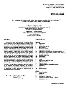
TABLE I T IMING C OMPARISONS BETWEEN OUR MPS O C EMULATION FRAMEWORK AND THE CYCLE - ACCURATE MPARM SIMULATOR
Matrix (one core) Matrix (4 cores) Matrix (8 cores) Dithering (4 cores-bus) Dithering (4 cores-NoC)
Fig. 3.
HW and SW flows included in the MPSoC Emulation Framework
MPARM 106 sec 5’ 23 sec 13’ 17 sec 2’ 35 sec 3’ 15 sec
MPSoC Emulation 1.2 sec 1.2 sec 1.2 sec 0.18 0.17
obtained onto the screen. In case the designer wants to modify the executed application, no re-synthesis is required and in few minutes another application can be tested in the proposed emulation framework. VI. E XPERIMENTAL R ESULTS
MPSoC system: processing cores, memory subsystem and interconnection to the main memories. This is done by instantiating, in a plug-and-play fashion, the predefined HDL modules available in our repository for each of the previous three levels (see Section III). For a complex MPSoC architecture with 8 processors and 20 additional HW modules, this step requires few hours. In the second phase, the range of parameters to be explored at each level and included HW instance is defined. This process can be done in few minutes thanks to our use of parameters in the instantiated modules. In the third phase, the designer specifies which HW components are the targets of the statistics extraction and connects adequate sniffers to each of them. This phase requires less than one hour in real-life MPSoC designs. Finally, in the fourth phase, the whole MPSoC HW platform is synthesized with the standard tool provided by the concrete FPGA supplier used. In our case we use the Integrated Software Environment (ISE) from the EDK Xilinx toolflow [11]. The synthesis process of our framework for a complex MPSoC system (i.e. 30 elements) takes approximately half an hour for the first time it is performed, but modifications in the current configurations of some cores take no longer than some minutes to be resynthesized. Overall, the whole process of creating the HW component of a complex MPSoC architecture requires no more than few hours within our emulation framework. Related to the SW flow, the first phase is the programming of the application to be used in the final MPSoC system. In our case, the Xilinx EDK tool used for the SW phase includes GNU C (gcc) and C++ (g++) compilers/linkers for the Power PC and Microblaze cores available in our repository. Thus, if the application to be tested is already written in any of these languages, no effort (and time) is required for the designer since the memory hierarchy and the utilization of the interconnection mechanism (e.g. generation of OCP transaction for the NIs of the NoC) are transparently generated by the underlying emulated HW architecture. In the second phase, the SW is compiled and binaries are generated by the EDK framework for each processor. In case of run-time errors, the system includes ported versions of the GNU gdb debugger. The compilation of the SW part of an 8-processor emulation system only takes minutes. Finally, in the last phase of the construction of the MPSoC emulation framework, the HW and SW components are uploaded onto the Xilinx FPGA-based platform using a JTAG device. Once the configuration of the overall MPSoC platform is finished, the system runs autonomously while the statistics are concurrently extracted and sent to the host PC. Then, our provided graphical interface running onto the host captures the packets sent and displays the statistics
144
We have assessed the performance and flexibility of the proposed emulation framework in comparison with the MPARM framework [3] by running several examples of multimedia applications in MPSoC architectures. In our experiments MPARM is executed on a Pentium IV at 3.0 Ghz with 1 GByte SDRAM and running GNU/Linux 2.6. In the first set of experiments we have evaluated the speed-ups that can be obtained by the emulation framework in comparison to cycle-accurate simulators. To this end, we have defined a simple SoC architecture composed by one Power PC core and our own bus using the protocol and latency of the AMBA bus. The memory hierarchy is composed by a L1 D-cache, I-cache and scratchpad memories, and an SRAM main memory of 32 MB. L1 memories sizes are evaluated in the range 2-16 KB, without relevant variations in the required time for the simulations/emulations performed. We have quantified the performance gains on a simple application, typical of multimedia processing, a matrix multiply processing core. Our results indicate (see Table I) that the emulation speed of our cycle-accurate emulation framework running at a real frequency of 100 MHz achieves more than 10 MHz (1.2 sec), including statistics extraction with 6 HW sniffers to cover the L1 memories, the memory controller and the traffic on the bus. However, the simulation speed of the cycle-accurate MPARM framework running on a 3 GHz processor is barely 125 KHz (106 sec). Thus, our emulation framework obtains an overall speedup of 88× while obtaining similar statistics as MPARM, e.g. total cycles spent by the processor, memory/scratchpad accesses, blockread/writes, simple read/writes, etc. (see Table II for a summary). Similar results were obtained with the soft-core Microblaze instead of the Power PC, showing that the inclusion of netlist softcores does not affect the performance of our emulation system, since they are not in the critical path of the virtual platform clocks. The second set of experiments has allowed us to evaluate how the emulated system scales when complex MPSoC architectures are explored. In this case, we have tested various configurations of interconnection mechanisms. We have instantiated a system with 4 cores (1 PowerPC and 3 Microblazes) and a complex L1 hierarchy for each core with 4 KB for D-cache and I-cache, 4 KB scratchpad and 16 KB of private memory. Then, two global main memories are shared between all processors of 1 MB using the OPB, OCP and our own bus. This whole system consumes 66% of the available space in the V2VP30 and runs at a platform frequency of well beyond 100 MHz. Next, we have explored the use of NoCs via the Xpipes Compiler [13] to replace the shared bus. The tested NoC configurations were composed of 2 32-bit switches with 4 inputs/outputs and 3-package buffers. The use of such a NoC topology with a sniffer in the
TABLE II E XCERPT OF STATISTICS EXTRACTED WITH THE EMULATION FRAMEWORK Metric Processor cycles Memory reads Memory block-reads Memory writes Scratchpad reads Scratchpad writes Cache read hits Cache read misses Fig. 4. Execution speedups of our MPSoC Emulation framework compared to the execution time of the cycle-accurate MPARM simulator
emulation system required 30%, using in the end 80% of our board for the whole MPSoC system. As SW driver, we have used a simple dithering filtering (around 300 lines of C code) using the Floyd algorithm [14] in two 128x128 grey images, divided in 4 segments and stored in the shared memories. This application is highly parallel and imposes almost the same workload in each processor, only slightly more in the last processor, which is in charge of merging the obtained results. This second set of experiments showed that the emulation system scales significantly better than SW simulation (see Table I). In fact, the exploration of MPSoC solutions with 4 cores (more than 30 HW components in total) and multiple bus-based interconnections, took 0.18 seconds (at 100 MHz) in the emulation platform, but 155 seconds in MPARM (at 125 KHz), resulting in a final speedup of approximately 860× (see Figure 4 and Table I). Moreover, the exploration of NoC interconnections imposes more overhead in cycleaccurate simulators (see Table I) than in our emulation platform due to the additional signals to manage, which enables even more speedups. In this case, the evaluation of each NoC configuration to try to find the design that optimally uses the available bandwitdh to the two main shared memories avoiding the congestion present in the bus-based solutions, required even less time in the emulated system (0.17 seconds), while more than three minutes in MPARM (due to the overhead of cycle-accurate signal management). As a result, our HWSW emulation framework achieved an overall speed-up of more than three orders of magnitude (1140×), illustrating its clear benefits for the exploration of the design space of complex MPSoC architectures compared to cycle-accurate simulators. VII. C ONCLUSIONS MPSoC architectures have been proposed as a possible solution to tackle the complexity of forthcoming embedded systems. These new systems are very complex to design since they have to be able to run various complex applications (e.g. video processing, or videogames), while meeting several additional design constraints, such as real-time performance or energy consumption. Hence, new frameworks that enable designers to validate and explore the behavior of their MPSoC design solutions executing the aforementioned software applications in a fast and cycle-accurate way are required. In this paper we have presented a new FPGA-based emulation framework that enables the rapid extraction of a large range of statistics at three different architectural levels of MPSoC designs, i.e. processing cores, memory subsystem and interconnection mechanisms. The experimental results have shown that our proposed framework obtains detailed reports with an speed-up of three orders of magnitude compared to cycle-accurate MPSoC simulators. Moreover, the addition of more processing cores
145
Matrix (1 core) 1.3×10⁷ 0 32×103 256×103 4096×103 0 4064×103 32×103
and more complex memory architectures in our emulation framework suitably scales. Thus, almost no loss in emulation speed occurs, conversely to cycle-accurate simulators. VIII. ACKNOWLEDGMENTS The authors would like to thank Federico Angiolini for his help with X PIPES C OMPILER. This work is partially supported by the Spanish Government Research Grant TIN2005-05619 and a Mobility Post-Doc Grant from UCM for David Atienza. R EFERENCES [1] Aptix System explore, 2003. http://www.aptix.com. [2] ARM integrator AP, 2004. http://www.arm.com. [3] L. Benini, et al. Mparm: Exploring the MPSoC design space with SystemC. Journal of VLSI, September 2005. [4] N. Genko, et al. A Complete Network-On-Chip Emulation Framework. In Proc. of DATE, 2005. [5] G. Braun, et al. Processor/memory co-exploration on multiple abstraction levels. In Proc. of DATE, 2003. [6] CoWare. Convergensc and LisaTek product lines, 2004. http://www. coware.com. [7] M. Diaz Nava, et al. An open platform for developing MPSoCs. IEEE Computer, pp. 60–67, July 2005. [8] Emulation and Verification Engineering. Zebu Xl and ZV models, 2005. http://www.eve-team.com. [9] H. Engineering. Heron mpsoc emulation, 2004. http://www. hunteng.co.uk. [10] Xilinx Enterprise. Xilinx Virtex-II Pro FPGA and IP components descriptions, 2004. http://www.xilinx.com/publications/ products/v2pro/xc v2pro43.htm. [11] Xilinx Enterprise. Xilinx Embedded Development Kit (EDK), 2004. http://www.xilinx.com/ise/embedded/edk docs.htm. [12] M. Graphics. Platform express and primecell, 2003. http://www. mentor.com/. [13] A. Jalabert, et al. xpipescompiler: A tool for instantiating application specific NoC. In Proc. DATE, 2004. [14] R. W. Floyd, L. Steinberg. An adaptive algorithm for spatial gray scale. In Proc. of ISDT, 1985. [15] A. Jerraya and W. Wolf. Multiprocessor Systems-on-Chips. Morgan Kaufmann, Elsevier, 2005. [16] ARM. PrimeXSys platform architecture and methodologies, white paper. Technical report, 2004. [17] P. Mishra, et al. Proc.-mem. co-exploration driven by an architectural description language. In Proc. ICVLSI, 2001. [18] P. G. Paulin, et al. Stepnp: A system-level exploration platform for network procs. IEEE D & T of Computers, 2002. [19] Synopsys. Realview Maxsim ESL environment, 2003. http://www. synopsys.com/. [20] Cadence Palladium II, 2005. http://www.cadence.com. [21] A. Wieferink, et al. A generic toolset for SoC multiprocessor debugging and synchronization. In Proc. ASAP, 2003.