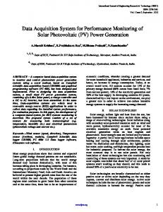
The online monitoring and control interface run on a local workstation which pilots .... have a full UNIX operating system which handles disks, tape writing and ...
A Data Acquisition System for Silicon Microstrip Detectors O. Adriani1 , G. Castellini2 , C. Civinini1 , R. D’Alessandro1 , M. Meschini1 , M. Pieri1 1 University of 2 Istituto
Florence and INFN-Firenze, Lgo. E. Fermi, 2, I-50125 Florence, ITALY Ricerca Onde Elettromagnetiche and INFN-Firenze, I-50125 Florence, ITALY
Abstract Following initial work done by some of us on the readout of the L3 silicon microvertex detector, we have developed a complete data acquisition system for silicon microstrip detectors for use both in our home institute and at the various test beam facilities at the CERN laboratory. The system uses extensive decoupling schemes allowing a fully floating connection to the detector. This feature has many advantages especially in the readout of the latest double-sided silicon microstrip detectors.
I. I NTRODUCTION Stimulated by the needs of two different collaborations, namely CMS [1] and PAMELA [2], we have developed a portable data acquisition system for the silicon microstrip detectors which are being designed in our home institute for the tracking sections of both experiments.
II. A NALOG F RONT- END R EQUIREMENTS
1 for each silicon face Fast hold FLOATING SECTION ECL decoupler
Fast hold
Control Signals
ADC Strobe
OptoCouplers
FIFO Strobe
Trig. in
Serial (RS 232)
SEQUENCER
PREMUX MOTHERBOARD +SILICON
Analog out Differential Buffer
FLASH ADC 10 bit Opto-couplers
FIFO MODULE BUFFERING FOR UP TO SEVEN ADCs (10 bit) DATA SERIALIZATION
Serial DataBus VME INTERFACE
(8 lines) VME BUS
VME CPU 1
VME CPU 2
DISK or TAPE
WORKSTATION Serial (RS 232) VSB BUS EVENT BUILDER CRATE
In figure 1 we show a global overview of the whole readout chain. The system is based on VME and uses standard VME CPUs for data formatting and for storage on both tape and disk. Signals from the silicon front-end amplifiers are converted and buffered locally. Data transmission to the VME CPU is concurrent with the digitization thus reducing transmission overhead. A custom designed sequencer based on the MAX7000 chips by ALTERA corp. provides all the necessary control signals to the front-end analog multiplexers. Furthermore the sequencer has a serial RS232 input through which a limited number of variable parameters of the sequence can be set. The ADCs used are based on a low-power 20 MegaSample Flash ADC from Analog Devices. The online monitoring and control interface run on a local workstation which pilots the VME CPUs through use of TCP/IP sockets. A Motif interface further simplifies the running of such a system while the graphical display of the data is implemented using CERN’s PAW software.
DUAL PORT MEMORY
Figure 1 : Overview of the whole readout system for silicon microstrip detectors.
We currently use both single-sided and double-sided detectors with different geometries and strip arrangements. These detectors have an analog front-end which so far has been either the VA-1 [3, 4] or the PreMux [5] developed for CMS tracking. These chips have 128 preamplifier channels with sample and hold, and a multiplexed single output. While the two chips have very different preamplifier characteristics, the analog multiplexers have similar switching times, namely in the 1�s range, and so, apart from small differences in the control lines and sequences, they are both driven by the same logic. Since double-sided readout is a must, we have decided to decouple electrically the front-end hybrids from the rest of the readout using optocouplers. This together with the use of floating power supplies, allows us to refer the analog boards to the bias voltages used for the silicon polarization. In this way no electrical stresses are placed on the decoupling capacitors used between the strips and the preamplifiers inputs (fig.2). This is an important feature of the system since the decoupling capacitors are delicate structures directly integrated on the detector which are not able to tolerate high electric fields. The multiplexer analog signal is fed straight to the ADC which is also referred to the bias voltages and which has optocouplers on its digital outputs. The readout time is, in our case, limited by the multiplexing circuitry which in the case of a full sized detector (1024 strips) using eight chips is in the 1ms range. The global readout speed has then been scaled accordingly to this limit. This relatively
IV. S EQUENCER
AMP. P-SIDE SUPPLY AMP.
TO MUX P-SIDE
Signal decoupling capacitor
P-SIDE STRIPS
BIAS VOLTAGE
SILICON BULK N-SIDE STRIPS
Signal decoupling capacitor
AMP.
TO MUX N-SIDE
AMP. N-SIDE SUPPLY
Figure 2 : Biasing scheme for a silicon detector and its readout circuitry.
comfortable speed has allowed us to use serial lines for data transmission to the VME system thus minimizing the number of cables.
III. A NALOG
TO
D IGITAL C ONVERTER
Number of Strips
Variable Freq. Clock Delay
Serial line RS232 From DAQ Crate
Strip Counter Stop
Multiplexer's Clocks φ Token In
1 φ2
To F.E. Chip
The components (SMD packages) are placed on both side of the 4 layers custom designed board; the digital ground, the analog ground and the power planes are well separated, and all the reference signals are placed on the same side of the board, thus obtaining both a reduction of spurious interferences and an overall improvement in performance.
Receiver
The conversion signal coming from the sequencer and the 10 bits digital output from the ADC are optically decoupled by means of fast TTL optocouplers from Hewlett Packard (HCPL7100 and HCPL0600), in such a way that all the ADC board is electrically referred to the bias voltage used for the sensors. With respect to the use of capacitors this method of decoupling has the big advantage as to completely minimize the risk of pick-up noise, coming from the digital lines, thanks to the very small parasitic capacitance (�1 pF) between input and output sections of the optocoupler.
20 Mhz Clock
Front-End Signal Generator
The differential analog signal coming from the front end analog bufferspis received by a wideband (275 MHz) low noise (7 nV/ Hz ) transconductance amplifier MAX435, from Maxim Integrated Products, which does not require any external negative feedback, thus allowing the use of long input cables while keeping the wide safety margin concerning system instabilities. The signal is then summed with a constant reference level and sent to the analog input of the ADC.
Serial In
Parameter Decoder
The converter board used in our system is based on a 10 bit CMOS ADC (AD876, from Analog Devices), which is well suited for our purposes; having a maximum sample rate of 20 Msample/sec, with low power consumption (140 mW), and wide full power input analog bandwidth (250 MHz); moreover, the chip has an internal input sample and hold amplifier.
The sequences needed for the correct driving of the analog front-end chips we use, are by and large fairly simple ones. The PreMux chip for instance just requires one token-in signal and two clock lines (�1 , �2 ) for the output shift register. As already stated before, we have based our system on the ALTERA family of chip devices. This has enabled us to fit the sequencer needed for our applications in one single MAX7000 (fig.3). The sequencer has TTL outputs which provide the necessary control signals for the analog multiplexers. Upon trigger assertion the programmed sequence starts with a token signal for the multiplexers shift registers. Concurrently a clock signal is given. The sequencer also strobes the ADC and the write line for the FIFO buffers. The output control lines from the sequencer are decoupled using optocouplers like the ADCs. The only exception to this optocoupling scheme concerns the trigger signal for the PreMux chip, which must be asserted 50ns after the passage of the particle in the detector; this is due to the very fast shaping time of the front-end amplifier. We were thus forced to use an ECL discriminator with decoupling capacitors. The price paid in terms of noise pick-up is not so high in this case, since this is a relatively quiet line coming from coincidence counters.
Write FIFO ADC Strobe
Trigger
MAX EPM 7160LC84-12 Programmable Logic Chip
Figure 3 : Block diagram of the sequencer board.
We have implemented a certain number of settable parameters, the setting of which is fulfilled by 5 bytes sent through a normal RS232 interface (also residing on the MAX7000). These parameters control the clock interval, the number of clock ticks (corresponding to the number of strips one wants to read), the ADC strobe delay with respect to the clock tick (usually determined by the multiplexer’s settling time) and the number of ADC strobes per clock tick (multi-sampling). The minimum tick period is 400 ns, in line with the speed characteristics of the analog multiplexers used so far.
V. DATA B UFFERING
AND
T RANSMISSION
The data coming from the ADC is immediately written in FIFO memories. The actual speed into the FIFOs is determined by the maximum PreMux’s multiplexer clock rate of 1 MHz.
VI. VME S YSTEM Our VME system consists basically of two MOTOROLA CPU boards (MVME 167, MVME162) with a custom made VME interface to the FIFO module. On the MVME167 we have a full UNIX operating system which handles disks, tape writing and networking, while the MVME162 is dedicated to running binaries downloaded from the other cpu. This configuration allows us to fully exploit the I/O capabilities of the system while keeping a friendly interface for the user. As a matter of fact all our data transfers and formatting are handled by the MVME162 which upon receipt of the trigger starts the appropriate procedures. The serial lines from the FIFO module are connected to our VME interface. This board is essentially nothing more than a serial to parallel converter which allows 32 bit data reads from the VME. The board is seen by the VME bus as memory locations through which data is accessed by simple read and write commands. A read instruction will start the serial transmission for 3 of the 8 FIFOs, and will take 1 �s. Triggers can be asserted on the MVME162 cpu in two ways, either with interrupts, or by continuos polling of an input register. Both methods are implemented although so far we have used the latter approach in our test beam runs. Data is buffered locally in the cpu’s 8Mbyte RAM and is written on disk/tape through the MVME167 cpu during out of spill time.
VII. C ONTROL
AND
M ONITORING
The entire data acquisition system can be controlled and monitored using a HP workstation. The main commands and parameters used to drive the various tasks running on the VME cpu’s, can be sent to the DAQ crate using tcp/ip sockets connecting UNIX based machines across the network. A Motif based interface has been built on the HP workstation for this purpose. This interface sends the initialization parameters to the sequencer, controls the main acquisition program on the MVME162 cpu (producer) and drives the disk/tape writing task that runs on the MVME167 cpu (consumer). In application where data should be sent to a main DAQ system (for example for integration in a test beam DAQ facility) data can be exchanged using dual port memories inserted in the VME crate or, if a MVME166 CPU is used, dual port memories connected via VSB bus. The logic block diagram of this system is shown
in figure 4. GRAPHIC DISPLAY X11
HP 712/60
MONITORING
UNIX
RUN CONTROL
TCP/IP SOCKETS ETHERNET
TCP/IP SOCKETS MVME 167
UNIX
MVME 166/162
VME BUS
DAQDAEMON
AAAAAAAAAAA AAAAAAAAAAA AA AA AA AA AA DEBUGGER
VSB INTERFACE
ACCESS VIA R/W INSTRUCTION ON VME-BUS
(FOR MVME 166 ONLY)
RS-232 SEQUENCER
INTERFACE TO THE FIFO ADC SYSTEM
VME BUS
PRODUCER
CONSUMER
SCSI BUS
DISK OR TAPE (LOCAL DATA STORAGE NFS MOUNTED)
Figure 4 : Overview of software components of the DAQ system.
A monitor program runs independently on the HP workstation reading streams of data directly from the network mounted VME disk. After the usual pedestal subtraction procedures we apply a clustering algorithm reconstructing the impact point coordinate of the particle on the detectors. The graphical output is displayed on the workstation using the CERN developed PAW program. In this way we are able to obtain almost immediate feedback on the data quality, allowing a much easier debugging of the detector setup. Strip Noise (ADC Counts) Strip Noise (ADC Counts)
We have chosen to use a parallel in serial out configuration for these memories, since this module is close to the ADCs but can be placed at quite a distance from the VME master crate. Having eight FIFOs with 9 bits each, the whole module can handle data coming from 7 ADCs with each FIFO having its own independent serial output. Data can be transmitted at a rate up to 100 Mbaud per line. On this module we have placed some control logic to handle the data transfer to the VME. For this purpose there are a few dedicated lines for the EMPTY and FULL signals and for handshaking. Again the logic is implemented in two MAX7000 allowing flexibility in case of changing future requirements.
12 10 8 6 4 2 0
20
40
60
80
100
120 Strip No.
200
250 Strip No.
12 10 8 6 4 2 0
50
100
150
Figure 5 : Single channel noise as function of strip number for the junction side (a) and ohmic side (b) of a double sided detector.
Figure 5 shows the single channel noise distribution for a double sided detector, as are obtained directly from the monitor
J-Side Charge (ADC Counts)
program. In figure 6 the charge correlation between the two sides of a detector, biased at 100 Volts, is displayed.
500
400
300
VIII. C ONCLUSIONS We have developed a data acquisition system that makes use of an extensive decoupling scheme allowing a fully floating connection to the detectors. This system is expecially suited for use with double sided detectors minimizing induced pick-up noise which frequently accompanies capacitive decoupling schemes. The system architecture has shown a high degree of flexibility being easily integrated with different read-out systems of various test beam facilities and used with two kind of front end electronics. The detailed schematics and functional description of the modules used can be obtained from ref. [6].
200
IX. R EFERENCES 100
100
200
300 400 500 600 Ω-Side Charge (ADC Counts)
Figure 6 : Charge correlation for a double sided detector obtained with particles entering the detector at normal angle (� = 0).
[1] The Compact Muon Solenoid, “Technical Proposal”, CERN/LHCC 94-38 LHCC/P1, 15 December 1994. [2] R. Bellotti et al., Pamela Technical report, DFF240/11/95. [3] F. Nygard et al., NIM A301, 1991 (506). [4] O. Toker et al., NIM A340, 1994 (572). [5] L. L. Jones, “PreMux128 Specification, version 2.1”, RD20 internal document. [6] O. Adriani et al., “A data acquisition system for silicon microstrip detectors”, Dipartimento di Fisica e INFN Firenze Preprint DFF 237/11/95.