Abstract. A divide-down rf source system has been designed and built at Argonne National Laboratory to provide har- monically-related and phase-locked rf ...
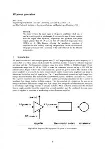
A DIVIDE-DOWN RF SOURCE GENERATION SYSTEM FOR THE ADVANCED PHOTON SOURCE D. Horan, F. Lenkszus, R. Laird Advanced Photon Source, Argonne National Laboratory 9700 South Cass Avenue, Argonne, Illinois 60439 USA Abstract A divide-down rf source system has been designed and built at Argonne National Laboratory to provide harmonically-related and phase-locked rf source signals between the APS 352-MHz storage ring and booster synchrotron rf systems and the 9.77-MHz and 117-MHz positron accumulator ring rf systems. The design provides rapid switching capability back to individual rf synthesizers for each one. The system also contains a digital bucket phase shifter for injection bucket selection. Input 352MHz rf from a master synthesizer is supplied to a VXIbased ECL divider board which produces 117-MHz and 9.77-MHz square-wave outputs. These outputs are passed through low-pass filters to produce pure signals at the required fundamental frequencies. These signals, plus signals at the same frequencies from independent synthesizers, are fed to an interface chassis where source selection is made via local/remote control of coaxial relays. This chassis also produces buffered outputs at each frequency for monitoring and synchronization of ancillary equipment. 1 RF SOURCE SIGNAL REQUIREMENTS The APS positron accumulator ring (PAR) uses two rf systems, operating at 9.77 MHz and 117.30 MHz (12th harmonic). These frequencies must be phase-locked to themselves and to the booster-synchrotron frequency of 351.930 MHz. For proper injection, maximum allowable jitter between the source frequencies is approximately 70 ps p-p [1]. In the PAR low-level rf systems, the phase of both the 9.77-MHz and 117.30-MHz signals is shifted to enable bucket-selection in the booster synchrotron during the injection cycle. This phase shifting is achieved by using separate calibrated analog phase shifters in the lowlevel rf signal paths or by shifting the phase of the rf source driving each PAR rf system. These source signals can be generated either by separate rf synthesizers or by a divide-down rf source generator board which divides the 351.93-MHz booster synchrotron source frequency into the two PAR frequencies and provides digitally-clocked phase shifting of the PAR frequencies. The separate rf synthesizers are supplied an external 10-MHz timebase signal distributed from a multiple-output master 10-MHz oven source. PAR rf source selection between the independent synthesizers and the divide-down generator board is provided by an interface chassis which uses coaxial relays for rf switching and also contains filtering and buffering for the divide-down generator outputs.
0-7803-4376-X/98/$10.00 1998 IEEE
2 DIVIDER BOARD DESIGN The divide-down rf source generator is a VXI-based ECL digital divider board (see Figure 1) which divides a 351.93-MHz sinewave input signal into 117.30-MHz and 9.77-MHz signals that are phase locked to each other and to the 351.93-MHz source. The board provides both CW and phase-shifted outputs at each PAR frequency and enables remote programming and control of the phase shift commands for storage ring bunch fill pattern control via the APS EPICS control system. A block diagram of the divide-down rf source generator board is shown in Figure 2. The 351.93-MHz input signal is transformercoupled to an ECL zerocrossing detector where it is converted to a 351.93-MHz square-wave. This signal is fanned-out and used as a timing clock to synchronize the digital phase shifters for each frequency and is also applied to the input of a programmable binary counter that performs a divide-bythree function and produces a 117.30-MHz square-wave Figure 1: Digital rf signal. This 117.30-MHz source generator VXI square wave is fed to the module. input of another programmable binary counter to divide the signal by 12 and produce the 9.77-MHz squarewave output. The 9.77-MHz and 117.30-MHz outputs of the dividers are fanned out to feed CW signals to the front panel connectors and to drive the input of a digital phase shifter for each frequency. The digital bucket phase shifters consist of independent clocked programmable shift registers that execute preprogrammed output phase shifts upon receipt of a “load phase” command. Using separate command steps, the phase-shift specification (bucket selection) is pre-loaded into the programming registers of the phase shifters, and then the phase shift is executed at the appropriate time during injection. The 117.30-MHz and 9.77-MHz phase shifters are capable of 3 and 36 possible output phase selections, respectively. At the present time during accelerator operation, only 12 selections are used.
2926
Figure 2: Digital rf source generator board diagram. The CW and phase-shifted square-wave outputs at 9.77 MHz and 117.30 MHz are passed through programmable delay generators to provide in-phase signals at the board output connectors. The output signals are fed to the front panel connectors through buffers which provide NIM and AC-coupled 50-ohm outputs at each frequency. Circuit board foil layouts use a combination of stripline and microstrip construction techniques to correct for propagation delays which would introduce timing errors. 3 SYSTEM INTEGRATION The divider board outputs are interfaced to the existing PAR low-level rf systems by a chassis which provides 9.77-MHz square-wave input signal
9.77-MHz low-pass filter
essential filtering, amplification, and switching (see Figure 3). This enables operation of the PAR rf systems using either the divide-down source generator or individual rf synthesizers as the rf source signals and either the analog or digital bucket phase shifters. The 9.77-MHz and 117.30-MHz square-wave rf source outputs of the divider board are low-pass filtered immediately upon entry to the interface chassis, using filters which have a minimum -60 dB rejection from 19.54 MHz and 234.4 MHz to 352 MHz, respectively, to resolve the fundamental component of each signal. At both PAR frequencies a coaxial relay switches either the CW output, if the downstream analog bucket phase shifter is to be used, or the phase-shifted divide-down rf source output to the input of the PAR low-level rf system through a leveling amplifier to insure constant rf drive amplitude. Again, at both PAR frequencies, another coaxial relay allows a stand-alone rf synthesizer to supply rf drive to the low-level rf system. Cable lengths are adjusted and attenuators provided to minimize the phase shift between source and phase shifter selections. Buffer amplifier/splitter networks are provided to supply multiple isolated rf outputs at each PAR frequency for timing and test purposes. Remote control and status readback of the interface chassis is provided. 4 PERFORMANCE MEASUREMENTS The theoretical performance of the divide-down rf source in terms of relative phase jitter between the output signals and the 351.93-MHz input was expected to be on the order of 20 ps p-p. Such levels of phase jitter are below the capability of available measurement equipment
X2 splitter -13 dB atten
9.77-MHz phase-shifted square-wave input signal
9.77-MHz sine-wave signal from rf synthesizer
9.77-MHz low-pass filter
X2 splitter
X2 splitter level amp X3 splitter
180-deg phase shift
+20 dB amp
-6 dB atten
9.77-MHz +16 dBm output to MCR
9.77-MHz output to low-level rf system
117-MHz square-wave input signal
117-MHz phase-shifted square-wave input signal
117-MHz sine-wave signal from rf synthesizer
117-MHz low-pass filter
117-MHz low-pass filter
X2 splitter
spare 9.77-MHz outputs at +11 dBm
-10 dB atten
+20 dB amp
level amp X3 splitter
X2 splitter
117-MHz output to low-level rf system
Figure 3: Rf source interface chassis diagram.
2927
spare 117-MHz outputs at +13 dBm
and are well under the accelerator specification. The divide-down source system was initially tested on the PAR rf systems under beam conditions in the summer of 1996. Accelerator operation during that test showed no degradation in accelerator performance using the divide-down rf source. Measurement on the filtered rf output signals of the divide-down source system indicates the frequency division process contributes nothing significant to the overall phase noise level of the system (see Figures 4(a) and (b)). The estimated phase noise specification for ideal ECL dividers is approximately -148 dBC/Hz [2]. This is well below other unavoidable sources of phase noise in the rf systems, such as the 800-foot cable run and 20-dB trunk amplifier necessary to supply the booster synchrotron 351.93-MHz source signal to the input of the divide-down board at an adequate level (see Figure 4(c)). As can be seen in Figure 4(a) and (b), low-pass filtering of the 9.77MHz and 117.30-MHz divide-down board square-wave outputs proved adequate to attenuate harmonic components of the signals to acceptable levels. Using the digital bucket phase shifter for storage ring fill pattern control has resulted in more uniform bunch-tobunch charge in the stored beam. Figures 5(a) and (b) show the bunch charge uniformity measurements made on (a)
CENTER FREQ = 351.93 SPAN = 20 KHZ
(b)
(a)
(b)
Figure 5: Storage ring bunch charge uniformity (a) analog bucket phase shifter, and (b) digital bucket phase shifter. storage ring beam, using identical fill patterns. Figure 5(a) represents two separate storage ring fills where separate rf synthesizers were used for the PAR rf source signals, and downstream analog phase shifters were used for bucket selection during injection. Figure 5(b) is the same measurement on stored beam, using the same fill pattern, after using the divide-down rf source system and digital bucket phase shifters for bucket selection. 5 CONCLUSION
(c)
CENTER FREQ = 9.77 MHZ SPAN = 20 KHZ
FREQ SWEEP 5 MHZ TO 100 MHZ
The PAR divide-down rf source system has logged approximately 1500 hours of on-line accelerator use and has contributed to improvements in injection efficiency and bunch fill pattern repeatability. It also improves the long-term stability between the APS injector and storage ring, reducing overall fill time. Future improvements to this system include efforts to further reduce phase noise in the 352-MHz divider input signal.
(e)
(d)
FREQ SWEEP 100 MHZ TO 1 GHZ
CENTER FREQ = 117 MHZ SPAN = 20 KHZ
6 ACKNOWLEDGMENTS I would like to recognize APS RF Group technicians Ernie Cherbak and Gian Trento for their efforts in construction and installation of the divide-down rf source hardware. This work was supported by the U.S. Department of Energy, Office of Basic Energy Sciences, under Contract No. W-31-109-ENG-38. 7 REFERENCES
Figure 4: (a) 351-MHz source, (b) and (c) 9.77-MHz filtered divide-down rf source signal, (d) and (e) 117MHz filtered divide-down rf source signal.
[1] [2]
2928
Steve Milton, private communication. U. L. Rhode, Digital PLL Frequency Synthesizers – Theory and Design, Prentice-Hall, pp. 85-88, 1983.