ESSCIRC 2002
A Highly Flexible, Module-based SoC-Approach for VoIP-Applications Paul Fugger, Johann Graf, Christian Jenkner, Frank Müller, Erich Oitzl, Harald Walcher, Markus Waldner, Johannes Salzmann, Markus Steiner Infineon Technologies Design Center Villach, A-9500 Villach
[email protected]
Abstract A System on Chip (SoC) is presented, which is wellsuited for both conventional telephony via the Public Switched Telephone Network (PSTN) and Voice over Internet Protocol (VoIP). A highly flexible approach offers the possibilities to integrate several interface types, customizable by software download. Additional download capabilities facilitate the integration of voice-codecs for voice compression, algorithms for silent noise injection, far end line echo cancellation, and fax/modem termination. The modular design-style allows to reuse all major building blocks in future systems. The modular testconcept enables separated tests for all parts of the chip as well as configurable self tests for easy go/nogodecisions.
1 Introduction Digital communication has become a preferred way for both corporate and public interconnection, mainly due to the availability of high-quality packet networks, such as IP, and ATM (Asynchronous Transfer Mode). There is, however, a manifold of activities to converge data with voice communications. VoIP is most attractive, since the public internet offers low-cost pricing and ubiquitous availability.
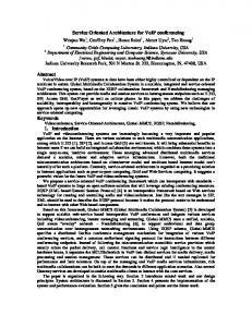
Figure 1. VoIP implementation Figure 1 [1] shows a scenario for a combination of VoIP with the conventional PSTN. It is conceivable that on the PC applications like answering machine (with an
acceptable recording time), or conference calls can be handled easily. Evidently, in the case of a cable network, all services like telephone, fax, video, and broadband data access can be provided over one network. The main challenge in applying voice communication within data networks is to provide a suitable Quality of Service (QoS). This includes: • Delay: If the end-to-end-delay is longer than about 250ms, talker overlap can occur. This means that one talker steps on the other talker’s speech. Since delay is mainly a bandwidth problem, voice compression can be applied to reduce the quantity of packets and/or the size of the packets. • Echo: This is well known from conventional telephony, many algorithms have been developed. Additionally, in IP-based systems longer signal runtimes cause the need for longer echo cancellation times, which directly influence DSP-performance and memory-size requirements. • Jitter (delay variability): In difference to PSTNtelephony no adequate synchronization mechanism can be provided by IP-based transmission. Clocks in different parts of a VoIP-system can diverge. Jitter buffers add artificial delay and can contribute to compensate these clock system differences. • Packet loss: IP-networks cannot guarantee that packets will be delivered at all. In the case of peak loads or congestion on the network, packets will be lost, since TCP-based retransmission is not suitable. Silent noise injection or even speech interpolation must be done in an intelligent way. Obviously all these methods have a huge impact on the performance requirements of the system. The algorithms for voice compression, echo cancellation, silent noise injection, or speech interpolation emphasize the need for high-performance DSP equipment. On the other hand, echo cancellation and jitter buffers require a huge amount of memory. Another application for IP-telephony is real-time fax transmission. To send faxes over packet networks, scan data must be converted to packet form, signalling and control protocols must be transformed and the complete delivery of the data in the correct order must be ensured. Packet loss and delay are even more critical here than in voice applications. Fax termination is a mandatory task for the DSP.
331
2 A Module-based SoC-Approach for VoIP
2.2 Design for Reuse
Benefits in terms of cost reduction and simplification of the networks could be the strongest driver for a widespread deployment of the VoIP-technology. Cost reduction can be accomplished either by merging the networks (to the cheapest one, the data network), as well as by increasing the integration density of the ICs. Infineon’s VINETIC (Voice and InterNet Enhanced Telephony Interface Concept) chip combines high integration with a number of advanced services for four lines of both PSTN- or VoIP-telephony.
The module-based approach allows easy design for reuse. This means that new chips can be customized, depending on the requirements of the customer. It is, for instance, conceivable to build a two-channel variant with reduced DSP-performance; on the other hand a 4-channel version might be needed, but without VoIP-features, thus reducing the DSP-performance requirements to a lower level again. Within a short time-span other variants of the chip can be created, enabling the evolution of a whole chip family with distinct features as well as different numbers of channels. Strict design-guidelines have been released internally, which aim to guarantee a high quality for future developments.
2.1 Chip Architecture The basic idea was to define a modular architecture to allow easy changes or extensions of the system. Therefore a bus-oriented architecture was chosen (see Figure 2).
Figure 2. VINETIC chip architecture All components can be accessed via the 16 bit FPIbus (Flexible Peripheral Interconnect bus; a derivative of the PI bus, which is a European Standard Bus. Also the ARM AMBA bus is a derivative of the PI bus). Possible masters are the DSP-subsystem, the PHI (Peripheral Host Interface), or the JTAG-interface controller. The codec-macros are responsible for the access to the analog high-voltage SLICs (Subscriber Line Interface Circuits). They include the AFEs (Analog Front Ends) as well as the digital high-frequency signal-processing in the hardware-filters and dedicated DSPs. The 2-channel granularity was chosen to facilitate the design of a twochannel variant of the chip. The PHI (Programmable Host Interface) is a dedicated proprietary RISC-controller with realtimemultitasking, which enables the management of several interface types by software. The DSP-subsystem combines a DSP (in this paper referred to as the DSP) with memory, and peripherals, like timers, power management unit, interrupt control unit, and emulation unit. In the current version Infineon’s Carmel with 140MHz is the main processor on chip.
332
2.3 Reuse of Designs The development of the VINETIC was alleviated by reusing several parts from predecessor chips on the one hand, and extensive use of IP (here: Intellectual Property) on the other. The DSP-subsystem is designed in a fully IP-based style. In the current version of the chip Infineon’s proprietary Carmel-DSP is used as a hardmacro. All peripherals as well as the FPI-bus components have been implemented as softmacros in VHDL. The main tasks of the designers of the DSP-subsystem have been to connect the delivered components and simulate them in the context of the whole subsystem. Due to the size (the DSP-subsystem contains more standard cells than all other components together) this is nevertheless a longsome task. Furthermore, it is well-known that the efforts for design validation of a system can be bigger than the sum of efforts for the original single components. Thus a “plug&play”-like design-style, which is always propagated by IP-providers, is only possible in terms of “plug”, but is in reality not true for “play”. The codec-macros have been implemented VHDLbased in similar kind for predecessor chips. Several extensions have been made, especially to allow accessibility via the FPI-bus system. Modifications in the hardware-filters allow more flexibility in programming the filter-characteristics. The system frequency of the AFE and the hardware-filters had to be raised mainly due to new capacitance parameters, which are caused by the migration to a smaller technology. The PHI was also taken from a predecessor chip and extended with regard to operating frequency, and memory size.
2.4 Flexibility and Programmability The emerging market for VoIP-telephony offers various fields of activities for DSP-software development. In particular the integration of voicecompression algorithms is of interest. The ITU-T (International Telephone Union, Telecommunication
standardization sector) and its predecessor, the CCITT (Comité Consultatif International Téléphonique et Télégraphique), have standardized several algorithms, like G.723.1, G.726 (ADPCM), G.728, G.729 (see e.g. [2], [3], [4], [5], note that in the nomination of the ITU they are referred to as speech codecs). Several other proprietary solutions exist, many of them including methodologies for voice interpolation and silent noise injection. To be prepared for both “old algorithms” as well as upcoming methodologies, all program memories in the DSP-subsystem are implemented as RAMs (except the boot-ROM and coefficient-ROMs), thus giving the software-guys a good facility to develop and test their programs. A simplified development-flow could look like the following scheme: • Write new software – typically a software-test in a chip-simulation is not possible, due to the necessarily long time that is needed to test voice compression algorithms. • Download the software via the PHI to the DSPsubsystem (see Figure 3 (a)). • Test the software in real-time on board (by the use of two analog ports the program can be made audible on the telephone receivers, see Figure 3 (b)). • Debug the software in the DSP-subsystem in the case of malfunction by using a special mode of the JTAGinterface (see Figure 3 (c), Section 2.5).
A feature that was adopted from predecessors, is the fully programmable filter-path. With more than seventy 4bit-coefficients and about hundred 16bit-coefficients, which are stored in the codec-macro coefficient-RAM (a coefficient-ROM stores default values), country-specific properties can be set, fulfilling all telephone standard requirements worldwide.
2.5 Testconcept Testing can be divided into two main sections: production testing and on-board-testing in the application. It is generally known that production testing is a timecritical task. Highest possible fault-coverage in the shortest possible time is the main target. Additionally, if faults are found during testing, comfortable analysis possibilities should be given to localize these faults precisely. These two facts encourage a modular test concept on the one hand, and nevertheless a high fault coverage on the other. Table 1 shows the most important out of 16 possible testmodes. Table 1. Production testmodes Testmode ATPG codec-macro/PHI ATPG DSP-core ATPG DSP-peripherals DSP memory-test PHI memory-test Codec-macro ROM-test via MISR Functional tests PLL-bypass (external master) PLL-test POR-test AFE-test (feed ADC/DAC out/in)
Group
Fast Production Tests
Analysis Test Capabilities
Figure 3. VINETIC algorithm development
The scantest was divided into 3 parts, giving a smaller overall ATPG-pattern (Automatic Test Pattern Generation). The dynamic behaviour of the chip is tested in the functional tests. Loop-back-switches at the interface between AFE and digital hardware-filters (see Figure 4, ALB and DLB) allow to test digital and analog parts separately. Thus a functional test of the digital parts can be accomplished without the need of costly analog evaluation.
Another key-aspect for future applications is a good programmability of the host interface. Currently seven interface types are included in the PHI. The parallel interfaces include Intel, Motorola, and HPI (Host Port Interface) protocols. The serial interface provides modes for PCM (Pulse Coded Modulation, referring to ITU-T recommendation G.711, see [6]), and IOM-2 (ISDN Oriented Modular interface, rev. 2). Additional programRAM is available, allowing the implementation of addons to the existing interface modes, or the definition of new ones.
Figure 4. Analog and digital loop back
333
PLL-bypass (tests run with external master-clock), PLL-test, PoR-test (Power-on Reset), and AFE-test enable an easy access to all analog components. That means that performance-measurements of the ADCs and DACs are possible, even if the digital part does not work. The overall fault-coverage is in the range of 98%. On-board-testing must provide possibilities for the customer to test the chip in the application. One necessary test is boundary-scan via JTAG-interface (Joint Test Action Group, the IEEE 1149.1 boundaryscan standard has been adopted industry-wide). A special mode in the VINETIC JTAG-interface allows to access the DSP-subsystem, and in consequence all other components via the internal FPI-bus. Additionally several debugging mechanisms, like breakpoints in the DSP-program, or register read-outs, can be accessed. A seminal test-methodology is the functional microtest. By the use of the DSP as FPI-master every configuration-bit of the chip (e.g. filter coefficients, power management mode, …) can be altered and readout with a downloaded program. Thus every smallest functional part of the chip can be tested individually, only depending on the DSP-software. In such a way it is imaginable to send a “virtual” signal (the DSP operates as a kind of function-generator) to one of the codecmacros (provided that the DLB is set, see Figure 4), get the response back from the hardware-filters and make an evaluation. Obviously, by extending the downloadable functional microtest program, every part of the chip can be tested, resulting in a detailed “error report”, that can be sent to the host via the PHI. This softwarepossibilities facilitate the implementation of self-test mechanisms with pass/fail-results.
3 Design Information A 0.18µm/1.8V (3.3V analog) technology (Infineon C10, fabricated at the plant in Essones) has been used. The whole design is described in VHDL, for synthesis/layout a Synopsys/Avant!-flow has been used. Static timing analysis and gatelevel-simulation with backannotation have been accomplished for final timing sign-off. The first silicon showed full functionality. Table 2 gives a summary of chip-specific details. Table 2. Chip-specific information System clock # transistors # macros # processors # memory
131.072 MHz 17.5 millions 67 (incl. 59 memories) 6 (incl. 1 hardmacro) 3.26Mbit (incl. 830kbit ROM)
Figure 5 shows a chip photo. The analog parts can be found at the bottom and on the top. At the left side, in the middle, the DSP-hardmacro can be seen. The memories for the DSP-subsystem (2.5Mbit) are located on the right side and above the DSP-hardmacro. The standard cell
334
part, which contains DSP-peripherals, PHI and the digital parts of the codec-macros are in the middle of the chip.
Figure 5. VINETIC chip photo
4 Conclusion A module-based SoC-approach for VoIP-applications has been presented. The chip, which is built in a 0.18µm/1.8V technology, offers a highly flexible fourchannel solution for telephony via both PSTN and VoIP. The flexibility in accessing the chip with different interface modes, and program download capabilities for all embedded processors and controllers, give the possibility to support state-of-the-art telephone algorithms and allow the easy implementation of future VoIP voice compression algorithms.
5 References [1] Ryan, J. “Voice over IP”, www.techguide.com, 1998. [2] ITU-T, “G.723.1 Dual Rate Speech Coder for Multimedia Communications transmitting at 5.3 and 6.3 kbit/s”, 1996. [3] CCITT, “G.726 40, 32, 24, 16 kbit/s adaptive differential pulse code modulation (ADPCM)”, 1990. [4] CCITT, “G.728 Coding of Speech at 16 kbit/s using Low-Delay Code Excited Linear Prediction”, 1992. [5] ITU-T, “G.729 Coding of Speech at 8 kbit/s using Conjugate-Structure Algebraic-Code-Excited LinearPrediction”, 1996. [6] ITU-T, “G.711 Pulse code modulation (PCM) of voice frequencies”, 1988.