A Low-Speed BIST Framework for High-Performance Circuit Testing H. Speek H.G. Kerkhoff MESA+ Research Institute, Univ. of Twente Testable Design and Testing of Microsystems Enschede, The Netherlands
[email protected]
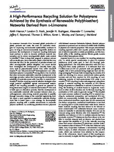
M. Shashaani M. Sachdev University of Waterloo Dept. of Electrical and Computer Engineering Waterloo, Ontario, Canada N2L 3G1
[email protected]
Abstract Testing of high performance integrated circuits is becoming increasingly a challenging task owing to high clock frequencies. Often testers are not able to test such devices due to their limited high frequency capabilities. In this article we outline a Design-for-Test methodology such that high performance devices can be tested on relatively low performance testers. In addition, a BIST framework is discussed based on this methodology. Various implementation aspects of this technique are also addressed.
1.
Introduction
The clock speed of advanced CMOS VLSI devices has surpassed the 1 GHz barrier. The Semiconductor Industry Association (SIA) roadmap for semiconductors 1997, expects even more aggressive increase in clock frequencies for future CMOS VLSI generations. However, testing and reliability of such devices is identified as one of the most critical challenges for VLSI testing [1]. In the past, testers had a timing accuracy of 5 times over the state of the art ICs. As a result, performance testing was not an issue. Since then, IC clock frequencies have improved on an average 30% per year while tester accuracy has improved only 12% per year. If this trend continues, tester timing accuracy will soon approach the cycle time of advanced devices. Long before such a situation arises, yield loss due to insufficient accuracy of the tester will become unacceptably high [1,2]. Figure 1, which plots the SIA roadmap 97 data, further illustrates the point. According to these numbers, inadequate tester resolution is causing undesirable yield loss in the state of the art, high performance VLSI. Cost of a state of the art tester has risen significantly and it costs approximately $4-5 Million. Its cost is expected to increase in years to come. In less than a decade, a high-end tester may cost more than $20 Million.
0-7695-0613-5/00 $10.00 ã 2000 I
Figure 1. Trends in the silicon clock period and the overall tester accuracy (OTA) [1,2]. The SIA roadmap predicts that cost of testing a die will surpass its manufacturing cost in the near future. The clock frequency of the device under test (DUT) plays a strong role in determining the overall test cost. Test cost can be reduced if the DUT can be tested at substantially lower frequency than its nominal frequency while ensuring its high frequency behaviour. The current BIST techniques are inadequate to test high performance devices. This is mainly due to the fact that the BIST is usually conducted at low frequencies. In section 4, a BIST approach will be presented which operates at low clock frequencies to detect the delay faults otherwise only detectable at high clock frequencies.
2.
Review and Motivation
Manufacturing defects are often divided into catastrophic and non-catastrophic categories. Catastrophic defects influence the IC topology significantly such that their influence is noticeable even at lower frequency. The impact of non-catastrophic or parametric defects is subtle and often means such as IDDQ, burn in, and performance testing are employed to uncover them. There is a general consensus among experts that large number of defects leads to reliability failure in the field. Although IDDQ testing and burn-in are very effective, their limitations are
becoming prominent as we march into the deep submicron regime [3-5]. A number of recent studies show concern about new failure mechanisms in scaled geometry that may be harder to detect with conventional means. Recently Nigh et al. [6] reported a significantly large number of timing only failures. These failures did not influence the circuit’s steady state logic functionality. Hence, these defects were not detected by slow speed stuck-at based or functional or BIST tests. Similarly, for Intel’s manufacturing process, Needham et al. [7] reported an increasing shift towards soft defects as technology moved from 0.35 to 0.25µm. These defects do not always cause failures at all temperature and voltage conditions. According to the authors, there is a correlation between soft defects and long-term reliability. Some of these defects can be detected by IDDQ testing provided background leakages are kept under control and ICs are designed to be IDDQ testable. In high performance ICs, dynamic circuit techniques and/or low transistors threshold (VT) technologies are often utilized. These techniques lead to either insufficient IDDQ coverage or make devices IDDQ untestable. For such ICs, performance testing and burn-in are routinely utilized to ensure longterm reliability. As cost of high performance testing is becoming expensive, researchers exploited innovative techniques to evaluate high frequency DUT response without a high-frequency tester. Agrawal and Chakraborty [8] divided them into indirect and direct test methods.
2.1.
Wagner and McCluskey [10] and Ho and McCluskey [11] found an empirical relationship between propagation delay at reduced supply voltage and the nominal supply voltage:
∆VDD + (1 − x)T0 T ’ = xT0 1 − k V0
Eq. 1
where T’ is the propagation delay at reduced VDD. T0 and V0 are nominal delay and nominal VDD voltage, respectively. The term k is a process-dependant constant and x is the fraction of the total path delay due to gate delay in the signal path.
2.2.
Direct Test Methods
Although correlation techniques are widely used in VLSI testing, these methods are still probabilistic in nature. In most applications, pass/fail decision-making based on such methods is hazardous [12, 13]. Direct test methods are generally preferred over indirect test methods. Direct methods include multiplexing of tester clock pins to extend the clock frequency range of a tester. Two or more high frequency clock signals are ORed to generate a higher frequency clock. This is a standard feature offered on most digital testers. Practical issues such as limited tester pins prevent from more than doubling of the original clock frequency.
Indirect test methods
The indirect test methods include correlation techniques to alleviate the need for high performance testing. Ring oscillators are often used for this purpose. A ring oscillator is put on a DUT and its free running frequency provides correlation to DUT high performance behaviour. Bruls [9] used an 11-stage on-chip ring oscillator as a performance indicator. The output of the ring oscillator was fed to a 10-stage counter to reduce the oscillation frequency from 200 MHz to 200 kHz. The free running frequency of the counter provided correlation for the DUT performance. Keshavarzi et al. [5] reported a strong correlation between IDDQ and the maximum operating frequency for a 32-bit microprocessor. They argued that these two parameters were fundamentally related, as both are functions of the channel length. This information can be used as a mechanism for high performance binning. CMOS digital circuits exhibit an increasingly large switching delay as supply voltage is reduced. In the limiting case, circuits work at VDD greater than the VT . If VDD is further reduced below VT circuits do not switch. Therefore, reduced supply-voltage testing may be carried out to lower the DUT operational frequency.
Figure 2. Pulse-triggered flip-flop and its clock waveform in normal and test modes [8]. Agrawal and Chakraborty proposed creation of a low frequency test mode in circuits. A quantifiable, externally controlled delay is added such that high performance testing can be carried out with relatively slow speed testers [8]. The basic idea of their scheme is illustrated in Figure 2. They proposed a (single-clock) pulse-triggered flip-flop with operational modes. In simple terms, a dynamic latch (highlighted pass transistor in Figure 2) was introduced inside a traditional master-slave flip-flop.
This three latches arrangement allowed modulation of flip-flop delay with the clock-pulse width. In a digital circuit, all signal paths must satisfy the timing relationship shown in Equation 2. Here, T denotes the clock period, PDFF the propagation delay through the flip-flop, PDCL the delay through the combinational logic, and TSetup the set-up time for flip-flops.
T ≥ PDFF + PDCL + TSetup
Eq. 2
Figure 2 also illustrates the clock timing in normal and test modes. In normal mode, increased pulse width of the clock increases the propagation delay of the flip-flop. Considering that PDCL and TSetup remain unchanged, the clock period, T, must become larger for Equation 2 to be valid. In other words, a slower clock frequency is able to test critical or other paths with the same timing specifications. This paper is an extension of the work presented in [12]. In this work we extend the concept of controlled delay flip-flop (CDFF) to realize a BIST scheme for high performance circuit testing.
3.
b) Figure 3. First controlled delay flip-flop (CDFF1): (a) block concept (b) its gate level implementation.
Flip-flop as a Controlled Delay Element
One of the most significant implementation issues in the pulse-triggered flip-flop is realization and propagation of a precise pulse width at the chip level. A small pulse width needed for high-speed normal mode operation may appear significantly distorted due to interconnect impedance. The dynamic latch, in addition, is rather time critical. However, an additional test mode clock can control flip-flop delay. We called these flip-flops controlled delay flip-flops (CDFFs). A CDFF differs significantly in concept and in implementation details from the pulsetriggered flip-flop. These differences are crucial and will become apparent to the reader subsequently in the article. Figure 3 illustrates a block diagram and a gate level implementation of the first CDFF (CDFF1). The CDFF1 has an additional input, the Test clock (Tclk). The slave latch receives a clock that is the logical NAND of the Clock (Clk) and the Test clock.
a)
Figure 4. Timing diagrams of normal mode operation (a) and the test mode operation (b).
Such an arrangement allows master to slave data transfer on the rising edge of Tclk. In the test mode, propagation delay through the flip-flop is controlled with Tclk. The significance of the Test clock is further illustrated with the help of Figure 4. This figure depicts the normal and the test mode timing diagrams of an arbitrary circuit with CDFFs. In the normal mode, Tclk has no function and is held high ensuring normal flip-flop operation (Fig. 4(a)). However, during the testing of an IC, it operates as a clock with tester-programmed time offset with the normal IC clock. The Test clock goes to all, or a pre-determined sub-set of flip-flops in an IC. This clock when active, controls the data transfer from master to slave latch in flip-flops. In the other words, depending on the timing relationship between the clock and Test clock, a delay is introduced between master and slave latches of the flipflop. The net effect is that flip-flop output Q appears after an additional delay, which is the time offset between the Clock and Test clock. Note that the synchronisation of the falling Clock edge with the end of the propagation time of the flip-flop tprop is purely accidental. Figure 4(b) illustrates the scenario when Tclk is active. In this condition, Equation 2 is modified as follows:
T ≥ PDFF + PDCL + TSetup + TOffset
controls the master to slave data transfer. The need for the second TG is to keep Q always in a driven mode [12].
Figure 5. Second CDFF (CDFF2) implementation. The result is a flip-flop with little additional transistors, not being time-critical and of which the delay can be well controlled.
Clk
Tclk Eq. 3
TOffset is time offset between the Clock and Test clock. The test mode clock period, TTM , should be large enough to accommodate all delay times listed in Equation 3. It is obvious from this equation that as the offset is increased the period of the clock is also increased or the clock frequency is reduced. In other words, the clock frequency can be reduced while the combinational circuit delays are tested with same delay margins. As compared to the pulse-triggered flip-flop, the implementation of CDFF1 requires 7 additional transistors and an additional test mode clock input. The timing, however, is less critical. Depending on the number of CDFF1s needed, a set of test clock buffers and interconnect lines may be required. The cost of implementation is high. Extra cost is compensated by cheaper, slower testers. The second implementation of a CDFF is shown in Figure 5. In this implementation two transmission gate pairs (TGs) are added, but the NAND gate mixing the clock and test clock line is removed. Effectively, the number of transistors is reduced with 2 in comparison with CDFF1. The first TG is added between master and slave latches while the second one is added in the feedback path of the slave. Both TGs are controlled by the Test clock. Addition of the first TG is obvious as it
Data
Q
0
20ns
40ns
60ns
80ns
Figure 6. Low-speed (20 MHz) HSPICE circuit simulation of the used CDFF2. The 0.35µm TSMC CMOS technology from MOSIS [14] has served as basis for our subsequent HSPICE circuit simulations. Figure 6 shows the behaviour of the circuit under low-speed testing circumstances (20 MHz) as to be discussed in the overall behaviour of the BIST structure in the next section. As can be seen, the input data becomes available at the output Q during the rising edge of the (delayed) Test-clock signal Tclk. Also at high clock frequencies, the circuit operated satisfactory. The CDFF2 has been used as the controlleddelay flip-flop in our BIST structure.
4.
A BIST Framework for Detecting Delay Faults
In the past, a number of papers have been published with regard to BIST for detecting delay faults [15-19]. Most efforts have been confined to generating the required two-pattern tests for detecting delay faults. The "adjacent testing" approach uses test pairs which only differ at a single position. As a result, simple hardware is required [15]. A more sophisticated technique starts with a predetermined set of test pairs, e.g. from ATPG, like in our case. Here, hardware is designed which generates sequences in which the test pairs (initialisation and propagation vector) are embedded [16]. The key elements in these generators are special Linear Feedback Shift Registers (LFSR) [17] or Multiple Input Signature Registers (MISR) [18]. Although rarely discussed, the evaluation of the responses can be carried out in a similar way as in "conventional" digital BIST approaches using signature analysers. A completely different approach makes use of controlled oscillation of the block involved [19]. However, the problem is measuring the high oscillation frequency either internally or externally. In our approach, additional hardware has been designed to carry out the BIST at low clock speeds [12, 20]. There is an option to include the above mentioned (partial deterministic) two-pattern generation and evaluation by means of MISRs (Full BIST) or choose for external application and evaluation by means of slowspeed (< 50MHz) ATE. The latter is sometimes referred to as Partial BIST. This paper is primarily focussed on the last option.
4.1.
Figure 7. Overall set-up of the BIST architecture. The transmission gates have been inserted for security reasons with regard to the OR-wired (buffered) output line. The decoder with addresses A0…A6 is a standard implementation of a 7-line-to-127-line decoder using NANDs. The decoder requires 266 transistors, and each of the 64 stages consists of 12 transistors. In total 1062 transistors are used.
Global set-up of the low-speed BIST
In Figure 7, the set-up of the BIST architecture is shown. Beside the full-BIST option employing MISRs for two-pattern generation and response evaluation, the key elements in the low-speed approach are the Programmable Delay Lines (PDL) and Duty-Cycle Control (DCC) blocks. As example, the test described in reference [12] has been used. In addition, the total system requires a number of registers, control logic and CDFF2s. Subsequently, the programmable delay line (PDL) and the duty-cycle control (DCC) blocks will be discussed in more detail. 4.1.1.
[21]. In our case inverter chains were used, tapped at uneven locations using NANDs as shown in Figure 8.
The programmable Delay-Line (PDL)
The most crucial part of the BIST architecture is the programmable delay line. There are several ways of implementing this structure, e.g. such as discussed in
Figure 8. Design of the programmable delay line. In a straightforward implementation of the PDL, the delay times are somewhat related to temperature, VDD and process variations. Using clever averaging / compensation techniques (see e.g. [20]) can reduce this influence, at the cost of increased complexity. An HSPICE circuit simulation was carried out to verify the behaviour of the circuit. The minimal timing resolution of the design was set to around 500ps. The maximum obtainable delay between the input and output becomes in this case 63.5ns. Figure 9 shows the lowspeed case (20 MHz) with a programmed delay of 12.5ns. Also in the high-speed case (130 MHz), with very little delay (500ps), the circuit worked satisfactory.
cycle test clock. It is clear from above that the PDL is the most complex part of the BIST structure due to the required delay and duty-cycle resolution. However, in practice some of the PDL parts can be combined. For the sake of simplicity this has not been implemented here.
In
Delay In
In (50%) 25ns
50ns
75ns
100ns
125ns
Figure 9. HSPICE circuit simulation of the PDL in the low-speed mode (20 MHz).
Out (95%) 20ns
4.1.2.
Programmable Duty-Cycle Control (DCC)
The second important component in the BIST architecture is the duty-cycle control (DCC) block. There are two DCC blocks required in the BIST architecture: one for the clock and one for the test clock. The simplest implementation consists of the previously discussed programmable delay line in combination with an advanced Set-Reset flip-flop as shown in Figure 10. The frequency range is between 10 and 50MHz, and the duty cycle can be varied up to 95% with a minimum pulse duration of 500ps. It requires 7 bits (A0 up to A6) to control this duty cycle.
80ns
120ns
Figure 11. Circuit simulation of the DCC in lowspeed mode (20MHz). Generated duty-cycle of 95%.
4.2.
Experimental Results
The previously described parts have been combined into the BIST architecture as depicted in figure 7. For the sake of simplicity and insight of the structure, the control parts and MISRs for signal generation and evaluation have been omitted in the simulations in Figures 12 and 13. Figure 12 shows the low-speed BIST in the fault-free case. The (combinational) logic [12] critical path has a delay of 4750ps. Verilog was used for the overall simulation, using HSPICE data for the different blocks. Clk Clk‘ Tclk Data_i To_lo Fro_lo
Figure 10. Design of the programmable duty-cycle control block, using the programmable delay line. The occupied chip area of the DCC is just slightly larger than half the area in the case of the PDL, because the last delay section is not required in the DCC. An HSPICE circuit simulation of this block for the low speed mode (20 MHz) and a duty cycle of 95% is shown in Figure 11. This range of values is also used in the overall BIST simulation using Verilog in the succeeding Figures 12 and 13. On top in Figure 11 is the 50% duty-cycle clock signal and at the bottom the generated 95% duty-
Data_o 50ns
150ns
250ns
Figure 12. Simulation of the BIST architecture in low-speed mode for fault-free behaviour. Delay: 4750ps. To_lo and Fro_lo indicate the data to the (logic) DUT and from the DUT respectively. Next, in Figure 13, the low-speed operation is simulated with values determined from simulations for the required frequency, duty-cycles and delay. For this delay fault, the frequencies are 20 MHz, duty cycles of clock and test clock 95.8% and 10.8% respectively, and a delay of 45ns between clock
and test clock. As can be seen from the simulations, the delay fault is detected in the last case. The simulations clearly show that the concept of low-speed BIST works. Clk Clk‘ Tclk Data_i To_lo Fro_lo Data_o 50ns
150ns
250ns
Figure 13. Simulation of the BIST structure in the low-speed mode detecting the delay fault. Delay: 5350ps. It is clear that still several refinements are required for reducing the structure’s susceptibility with regard to process and environmental variations. Also the proper MISR parameters have to be refined and the final design has to be optimised and will be based on 0.18µm CMOS technology.
5.
Conclusion
A new type of DfT structure and associated BIST architecture has been proposed for detecting delay faults in digital high-performance circuits. It circumvents the requirement of an expensive high-speed tester. Depending on the application, a full BIST or a DfT approach employing a low-speed tester can be used. Our BIST architecture and associated DfT hardware is based on a different concept as compared to previous approaches. The manipulation of delay between and duty cycles of the clock and an additional test clock as well as the use of new controlled delay flip-flops are crucial in this respect. Simulations of the DfT parts, as well as the overall architecture indicate the viability of our method.
References [1] [2] [3]
----, Semiconductor Industry Association (SIA) Roadmap for Semiconductors, 1997. G. Singer, "The Future of Test and DFT", IEEE Design & Test of Computers, July-September 1997, pp. 11-14. T. W. Williams, R. H. Dennard, R. Kapur, M. R. Mercer, and W. Maly, "Iddq Test: Sensitivity Analysis of Scaling", Proceedings of International Test Conference, 1996, pp. 786-792.
[4]
M. Sachdev, "Deep Sub-Micron IDDQ Testing: Issues and Solutions", Proceedings of European Design and Test, 1997, pp. 271-278. [5] A. Keshavarzi, K. Roy and C. F. Hawkins, "Intrinsic Leakage in Low Power Deep Submicron CMOS ICs", Proceedings of International Test Conference, 1997, pp. 146-155. [6] P. Nigh et al., "So What is an Optimal Test Mix? A Discussion of Test Sematech Methods Experiment", Proceedings of International Test Conference, 1997, pp. 1037-1038. [7] W. Needham, C. Prunty, E. H. Yeoh, "High Volume Microprocessor Test Escapes, An Analysis of Defects Our Tests are Missing", Proceedings of International Test Conference, 1998, pp. 25-34. [8] V. D. Agrawal and T. J. Chakraborty, "High-Performance Circuit Testing with Slow-Speed Testers", Proceedings of International Test Conference, 1995, pp. 302-310. [9] E. Bruls, "Variable Supply Voltage Testing for Analogue CMOS and Bipolar Circuits", Proceedings of International Test Conference, 1994, pp. 562-571. [10] K. D. Wagner and E. J. McCluskey, "Effect of Supply Voltage on Circuit Propagation Delay and Test Application", Proceedings of International Conference on computer Aided Design, 1985, pp. 42-44. [11] H. Ho and E. J. McCluskey, "Very Low Voltage Testing for Weak CMOS Logic ICs", Proceedings of International Test Conference, 1993, pp. 275-284. [12] M. Shashaani and M. Sachdev, "A DFT Technique for High Performance Circuit Testing", Proceedings of International Test Conference, 1999, pp. 276-285. [13] M. van Rosmalen, K Baker, E. Bruls, J. Jess, "Parameter Monitoring: Advantages and Pitfalls", Proceedings of International Test Conference, 1993, pp. 115-124. [14] http://www.mosis.org: MOSIS TSMC 0.35 CMOS process data. [15] P.Girard et al., "An Optimized BIST Test-Pattern Generator for Delay Testing", in VLSI Test Symposium, 1997, pp. 94-100. [16] C. Dufaza, Y. Zorian, "On the Generation of PseudoDeterministic Two-Patterns Test Sequence with LSFRs", European Design and Test Conference, 1997, pp. 69-76. [17] N. Mukherjee, T.J. Chakraborty, S. Bhawmik, "A BIST Scheme for the Detection of Path-Delay Faults", in Proc. International Test Conference, 1998, pp. 422-431. [18] M. Keim et al., "A Scalable BIST Architecture for Delay Faults", in Comp. IEEE European Test Workshop, Constance, 1999, pp. S5A 14-15. [19] K. Arabi et al., "Digital Oscillation-Test Method for Delay and Stuck-at Fault Testing of Digital Circuits", in Proc. International Test Conference, 1998, pp. 91-100. [20] H.G. Kerkhoff, K. van Nee, H. Speek, "DfT for DelayFault Diagnosis in Digital High-Speed ICs", in Comp. IEEE European Test Workshop, Constance, 1999, pp. SP4/5 9-10. [21] G.C. Moyer et al., "The Delay Vernier Pattern Generation Technique", in IEEE Jrnl. of Solid-State Circuits, vol. 32, no.4, April 1997, pp. 551-562.