Aware Voltage Assignment,â DAC, 2006, pp. 429â32. [7] R. Ching, E. Young, K. Leung and C. Chu, âPostâPlacement Voltage Is- land Generation,â ICCAD, 2006, ...
1B-5
A Multiple Supply Voltage Based Power Reduction Method in 3-D ICs Considering Process Variations and Thermal Effects Shih-An Yu
Pei-Yu Huang
Yu-Min Lee
Department of Communications Engineering National Chiao Tung University
Abstract— In this paper, a grid-based multiple supply voltage (MSV) assignment method is presented to statistically minimize the total power consumption of 3-D IC. This method consists of a statistical electro-thermal simulator to get the mean and variance of on-chip, a thermal-aware statistical static timing analysis (SSTA) to take into account the thermal effect on circuit timing, the statistical power delay sensitivity–slack product to be the optimization criterion, and an incremental update of statistical timing to save the runtime. The experimental results demonstrate the effectiveness of the developed methodology and indicate that the consideration of the thermal effect in the circuit simulation is imperative.
Netlist
Cell Library ( LEF/DEF )
Timing/Leakage Power Cell Library
3D Placement ( Bookshelf )
Statistical 3D Thermal Analysis Thermal Aware Statistical Timing Analysis Timing Violation
Yes
Rescue
No 3D IC Yes Voltage Assignment
Timing Budget No Post Tuning
Grouping and Extension End
I. I NTRODUCTION
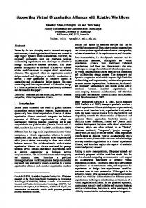
Fig. 1. The executing flow of this work.
Increased wire lengths and interconnect density of 2-D chip produce seriously parasitic effects which increase the circuit delay and the power consumption. The 3-D IC technology has been proposed to solve this problem. It allows the designer to stack dies vertically in the same package and connect components on different tiers by through-silicon vias (TSVs) [1]. Using 3-D ICs not only reduces the wire lengths but also improves the system integration. Nevertheless, due to the higher power density and the low thermal conductivity inter-layer dielectrics, the heat removal is an important issue in the 3-D IC design. The high temperature reduces the life time and reliability of device and impacts the circuit performance [1]. Since the power consumption of circuits is the source of thermal problem, making power reduction is a necessary step. In addition, due to the shrinking of device geometries, growing process variability of physical parameters has made the deterministic analysis and optimization at a prescribed process corner be no longer effective. The alternative approach treating delay/leakage power as random variables is the statistical timing and leakage power analysis/optimization. As shown in [2, 3], 30% process variations can cause up to 20× leakage power variations and the ratio of the leakage power to the total power has been increased 10 times from the 180 nm process to the 90 nm process. Hence, it is crucial to consider process variations in the power optimization work. In the existing power reduction techniques, MSV [5–7] can be used to reduce both dynamic and leakage power effectively because of the quadratic relation between the supply voltage and dynamic power, and the exponential relation between the supply voltage and leakage power. It provides the premium result with less penalty [4]. Our major contributions are summarized as follows. 978-1-4244-2749-9/09/$25.00 ©2009 IEEE
• We develop a post-placement MSV method with considering spatial correlated process variations and thermal effects for 3-D ICs. Compared with the previous works which solve the deterministic problems and use the thermal unrelated models, the proposed method is more flexible and practical. Moreover, this is the first work that discusses the voltage island generation in 3-D ICs. • In [8], the temperature was assumed to be independent of the circuit design and the temperature on each location was equal; however, the placement can affect the temperature distribution. Therefore, in our work, the temperature is treated as a random process related to the designed circuit, and can be incorporated into the SSTA without sacrificing the efficiency of SSTA. • Our proposed algorithm uses a heuristically incremental method to update the statistical delay to avoid performing SSTA for the whole circuit after each step or adjustment. The rest of the paper is organized as follows. The proposed statistical power optimization methodology is described in section II. In section III, the experimental results are given to support our methodology. Finally, conclusion is provided in section IV. II. M ETHODOLOGY The proposed power reduction design flow for 3-D ICs is shown in Fig. 1. Given a design placement of 3-D IC with its netlist and a standard cell library, the flow first executes a statistical electro-thermal simulation to obtain its statistical temperature distribution. After that, a thermal aware SSTA is
55
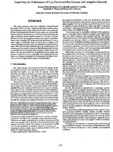
1B-5 Input: Fitted cell leakage power, Dynamic power, Placement, Spatial correlation function Output: The first order H-PCs expression of the 3-D ICs temperature distribution First stage 1. Parameter modeling by KL expansion 2. Build projected power cell library of each layer with supposed initial temperature 3. Use 1–D thermal model and average mean temperature to set the thermal parameter 4. Re–build the subthreshold leakage power library by average mean temperature repeat steps 2∼4 until the mean temperature converges Second stage 1. Obtain mean temperature by using 3-D deterministic GIT thermal simulator 2. Obtain the first order PC expansion of the multi–layer temperature distribution 3. Re–build the subthreshold leakage power library repeat steps 1∼3 until means and variances of temperature converge
performed with the statistical temperature distribution got from the previous step. The slack data provided by SSTA is used to compute the statistical power delay sensitivity–slack product; next, a grid-based procedure is executed to assign the supplied voltages. After the assignment procedure, the power consumptions and delays of gates are changed so the thermal and timing analysis are done again, and the circuit timing is verified. If there is any timing violation, a rescue procedure is enforced to assure the timing correctness and finish the iteration. When the circuit satisfies the timing constraint, the flow starts the assignment process again. The proposed method also terminates the loop when the iteration can not provide any improvement. Finally, a post-tuning step is employed to further lower the power consumption, and the grouping and extension steps are utilize to complete the voltage island generation. Each executing step is going to be described in the rest of this section. A. Statistical 3-D Thermal Analysis
Fig. 2. Algorithm of the statistical thermal simulation.
Generally, the dynamic power is insensitive to process variations and can be assumed to be deterministic. But the leakage power is greatly affected by physical parameters and need to be treated as random process [9]. Based on the empirical models [10,11], the gate leakage current Igate is related to the oxide thickness, and the subthreshold current Isub is related to the channel length and temperature. The leakage current models of gates can be built by using the least square fitting method to the estimating results of HSPICE under the 90 nm technology as follows. Igate
=
b0 exp (b1 tox ) .
(1)
Isub
=
c0 exp (c1 Lef f + c2 T ) ,
(2)
Our statistical electro-thermal aware 3-D IC thermal simulator extends the Hermite polynomial chaoses (H-PCs) based 2-D IC statistical thermal simulator [14,15] to the 3-D IC, and combines this extended 3-D IC statistical thermal simulator with the electro-thermal iterative updating loop. Due to the limitation of space, we only summarize the simulating flow of our statistical 3-D IC electro-thermal simulator in Fig. 2. By this procedure, the random process of 3-D IC temperature distribution T (r, θ, ω) can be approximated as the following first order H-PCs expression. T (r, θ, ω) ∼ = T0 +
tox (r) +
� �
βn fn (r)ςn (�),
B. Thermal Aware Statistical Timing Analysis The thermal-aware SSTA is developed by including thermal effect into the block based SSTA [16]. The gate delay is built as a canonical first-order form by applying the least square fitting method to the estimating results of HSPICE under 90nm technology and is stated as
(3)
n=1 NL
Lef f (r, θ)
≈
Lef f (r) +
ef f � √
χm qm (r)ζm (θ),
(5)
where Tk (r) is the projected temperature coefficient function. The above result can be used in our thermal-aware SSTA to calculate power delay sensitivity–slack product and to get the power density induced weights of grids in the successive steps.
Ntox
≈
Tk (r)ξk ,
k=1
where tox is the oxide thickness, Lef f is the effective channel length, T is the temperature of gate, and the fitting coefficients bi ’s and ci ’s are VDD dependent and a look-up table is set up to store them for each different VDD . With equations (1) and (2), the subthreshold and gatetunneling leakage powers of gates are Psub = VDD Isub and Pgate = VDD Igate , respectively. By applying the KL expansion to the spatial correlation function in [12], spatially correlated Lef f and tox are expressed as tox (r, �)
�
NKL
Delay = a0 + a1 Lef f + a2 tox + a3 T,
(4)
(6)
where ai ’s are VDD dependent fitting constants and a look-up table is built to store those coefficients for each different VDD . By using equations (3)–(6), the delay of a specified type of gate located at a specific location r∗ is
m=1
where r is the location of the die, tox (r) and Lef f (r) are the means of tox (r, �) and Lef f (r, θ), respectively, � and θ are the sampling values of tox (r, �) and Lef f (r, θ), fn (r) and qm (r) are eigenfunctions of tox (r, �) and Lef f (r, θ), βn and χm are eigenvalues of tox (r, �) and Lef f (r, θ), respectively. Ntox and NLef f are the truncated numbers of tox (r, �) and Lef f (r, θ), respectively. {ςn (�)} and {ζm (θ)} are mutually independent standard normal random variables since tox (r, �) and Lef f (r, θ) can be assumed to be independent Gaussian processes [13]. For the sake of notation simplicity, ξn , ςn and ζn are used to represent ξn (�, θ), ςn (�) and ζn (θ), respecNLch NTox KL tively, {ξn }N n=1 is set as the union of {ςn }n=1 and {ζn }n=1 , and NKL =NTox +NLch .
Delay = a0 + a1 Lef f (r∗ , θ) + a2 tox (r∗ , �) + a3 T (r∗ , θ, ω) �
= a0 +
�
NKL
(a1 qk∗ + a2 fk∗ + a3 Tk (r∗ )) ξk
k=0 �
= a0 +
�
NKL k=0
�
ak ξk ,
(7)
√ √ where qk∗ = χk qk (r∗ ) and fk∗ = βk fk (r∗ ). Equation (7) is consistent with the canonical first-order delay form in [16]. As a result, the thermal effect can be taken into account in the SSTA without any extra complexity.
56
1B-5 grid i. �
P DS–Sgridi =
P DS–Sgatej ,
(8)
gatej ∈gridi
where P DS–Sgatej is the power delay sensitivity–slack product of gate j and is defined as � def
P DS–Sgatej =
ΔPj ΔDj
Slackj ,
0,
Slackj ≥ ΔDj ; else.
(9)
Here, Slackj is the timing slack of gate j, and ΔPj and ΔDj are the power dissipation and the delay differences for providing the lower VDD instead of the higher VDD , respectively. For the purpose of the statistical power delay sensitivity– slack product computation and speeding up our power reduction flow, the fitting forms of ΔPj and ΔDj are precharacterized by using the least square method to fit the results of HSPICE simulation. Each ΔDj is fitted as the first-order form similar to equation (6) with respect to Lef f , tox and T . Each ΔPj is fitted as the exponential form similar to equations (1) and (2) with respect to Lef f , tox and T . With equations (3)–(5) and a similar derivation as equation (7), ΔPi and ΔDi for each gate i can be expressed as
Fig. 3. A three-tier design example of the grid-based procedure for generating the voltage islands. Each tier is divided into many grids, and the grid with the large weight has dark color.
C. The Proposed 3-D IC Voltage Island Generator All the tiers are needed to be simultaneously considered in the three dimensional voltage assignment procedure. An obvious reason is that the timing budget is limited. If the voltage assignment is performed tier by tier, the remaining timing budget will become less and less. This results in an ill circuit with power consumptions of layers is extremely unbalanced. For example, the power consumption may be acceptable for a region on a specific tier, but its upper or lower counterpart has high power consumption, which causes the thermal problem in the vertical space.
ΔPi = ΔPdynamici + ΔPsubi + ΔPgatei �N �N � � KL KL � � � � � � = pi0+ci0 exp cik ξk +bi0 exp bik ξk k=1
�
(10)
k=1
NKL
C.1
ΔDi = di0 +
The Proposed 3-D IC Voltage Assignment
dik ξk .
(11)
k=1
In the beginning, the timing budget of the circuit is checked. The program stops the execution when the timing budget is not enough; otherwise, the assignment procedure is performed. The voltage assignment is executed as follows. Each tier is partitioned into many grids, and the weights of each grid for assigning lower VDD is decided by three criteria: a) the statistical power delay sensitivity–slack product, b) the power density induced weight and c) the total number of sites. The next step is to vertically compress the three dimensional structure into a two dimensional planar, and the weights are accumulated for each compressed grid. After compressing, the priority of each compressed grid is decided by its accumulated, and the grid with the highest priority is selected. Then, the selected compressed grid is restored back to the multi-layer structure. This action is helpful for us to understand whether the accumulated weights are contributed by a grid on a specific layer or by all the grids on each layer averagely and to decide which grid for using the low supply voltage. Finally, all gates in this grid are assigned with the low supply voltages. A three-tier design example of the above grid-based procedure for the voltage assignment is illustrated in Fig. 3. Statistical Power delay sensitivity–Slack Product A low (high) supply voltage reduces (increases) the power consumption but slows (accelerates) the speed of gate. To utilize the timing budget effectively and achieve the most power saving, the statistical power delay sensitivity–slack product of each gate is used as the most important optimization-criterion. product of The power delay sensitivity–slack grid i (P DS–S gridi ) is the summation of the power delay sensitivity–slack product of each gate in
After executing the thermal-aware SSTA, Slacki can also be expressed as the following canonical first-order form. �
NKL
Slacki = si0 +
sik ξk .
(12)
k=1
With the definition of the power delay sensitivity– slack product in equation (9), the following statistical power delay sensitivity–slack product for each gate is applied in the power reduction flow and P DS–Sgatei is re-defined as �
�
P DS–Sgatei =
E 0,
ΔPi ×Slacki ΔDi
�
probi ,
probi ≥ η; else.
(13)
def
Here, probi = prob (Slacki ≥ΔDi ) and it can be obtained in constant time by table looking up to the tail probabilities of a normal random variable with μ = si0 − di0 and σ 2 = NKL 2 k=0 (sik − dik ) , and η is a user-specified threshold value. Because the complexity to obtain the exact value of E {ΔPi × Slacki /ΔDi } is very high, an accurate approximation with the runtime in O(NKL ) is obtained based on the second order Taylor approximation. By rewriting ΔPi × Slacki /ΔDi as a concise representation g(ξ), the second order Taylor approximation of E{g(ξ)} at expansion point ξ ∗ = 0 is E{g(ξ)} ≈ g(0) +
NKL 1 � ∂ 2 g(ξ)
. 2 ∂ 2 ξk ξ=0
(14)
k=1
KL Here, ξ is the set of {ξk }N k=1 . Equation (14) is due to the fact that E{ξk } and E{ξk ξj } for k �= j are zeros. The
57
1B-5 High
Tempperatture
uct of the power density of grid i with the weight of truncation regions which corresponds to grid j. Consequently, the accumulated value of each grid is the summation of the power density induced weights from itself and from the neighboring grids among tiers. Here, the power density of grid i is obtained by using μPTi + 3σPTi to ensure the thermal safety. PTi is the power consumption in grid i, and μPTi and σPTi can be computed by using the means and variances of powers of the types of gates in grid i. Substituting equations (3)–(5) into equations (1)– (2) and taking the mean and variance of equations (1)–(2), the mean and variance of the power for a type of gates in grid i can be got. For example, the mean and variance of the subthreshold leakage power for a type of gates in grid i can be formulated as
(a)
(b)
(c)
Low
Fig. 4. A three-tier chip example for constructing the experimental model of power density induced weights. (a) An 1W power is inserted into the grid (5, 5) on the tier 1 and the corresponding temperature profile on each tier. (b) An 1W power is inserted into the grid (5, 5) on the tier 2 and the corresponding temperature profile on each tier. (c) An 1W power is inserted into the grid (5, 5) on the tier 3 and the corresponding temperature profile on each tier. The color bar shows the related levels of the temperature with respect to the colors on tiers. The arrows indicate the 1W power sources. The rectangles with dotted line margins are the truncation regions.
�
E{Psub }
=
V ar{Psub }
=
� NKL 1 � 2 βk , 2 k=1 �N � KL � 2 2 cˆ0 exp βk , cˆ0 exp
(15)
(16)
k=1
where cˆ0 and each βk are known values consisting of VDD and the leading coefficients of ξk of Lef f and T (r, θ, ω) in equations (4)–(5).
statistical power delay sensitivity–slack product of a gate depends on the status of its logical neighbors as well as its slack, both of them can be change during the assignment procedure. Thus, the incremental updates on the timing and the statistical power delay sensitivity–slack product of a gate are needed and are described in section C.2.
Total Number of Sites The gate is called a site if its timing constraint is violated when the lower VDD is assigned to it. Hence, we must avoid generating too many sites during the assignment procedure. In fact, this criterion is related to the statistical power delay sensitivity–slack product. Because the site contributes zero P DS–Sgate , a grid i has high P DS–Sgridi should not contain too many sites.
Power Density Induced Weight The second important criterion is the power density induced weight among the compressed grids because the hot-spot issue must be avoided during executing the proposed power reduction method. The power density induced weights of grids are obtained as follows. Firstly, we make an experimental model for the power density induced weights. As shown in Fig. 4, an 1W power source is orderly inserted to the central gird of each tier and its corresponding temperature profiles of tiers are obtained. The above step is to approximate the spatial response of the heat transfer equation for a specified 3-D IC. Then, these corresponding temperature profiles are normalized in the range from 0 to 1 by using the maximum temperature among all of these corresponding temperature profiles. Finally, the truncation regions of these normalized temperature profiles are obtained by a specified threshold value. The above truncation regions can be pre-characterized before the placement because the spatial response for the heat transfer equation only depends on the package structure, chip dimension and the thermal parameters of a specified 3-D IC. Therefore, it can be re-used when the power reduction method is executed. Although the spatial response of the heat transfer equation for a specified 3-D IC are different among different locations, the weights in the truncation regions of grids are slightly different in our experimental result. For the efficiency, all of grids are set to share the same weights in their truncation regions in our implementation1 . With these truncation regions, the power density induced weight of grid j induced by grid i can be obtained as the prod-
C.2
Incremental Update
For reducing the computational load of performing the SSTA after every voltage assignment step , we develop an incremental approach to approximately update the sensitivity. The basic concept is borrowed from the STA. For example, the gate C in Fig. 5(a) has two input signals which are from the outputs of gate A and gate B. Given the arrival times of gate A and gate B being 2 and 5 by using the STA, respectively, the arrival time of C is determined by the latest arriving output B. When gate A is chosen to operate at the low supply voltage, and the arrival time of A increases to be 4, C is not affected because B is still the slowest input. Nevertheless, when the arrival time of A becomes 6, the arrival time of gate C is changed. In conclusion, the low supply voltage assignment can impact C only when the new arrival time exceeds the original dominated one. This similar concept can be extended to the statistical situation. In this example, the gate C records its latest arriving input M = M AX(A, B) as shown in Fig. 5(d) after the first timing analysis. When the low supply voltage is assigned to gate A, the arrival time of A is changed to A� . Then, we compare these two random variables. If prob(A� ≥ M ) ≥ α, where α is a user-defined bounded parameter, it means that gate C is heavily affected by this assignment. Therefore, the timing and P DS–SgateC should be updated, and the new latest arriving input becomes to M � = M AX(A� , M ). C.3 Site Rescue
1 To get a more accurate result, truncation regions with different weights can be obtained for the grids in the regions of the center and the corners of a specified 3-D IC.
Although the grid with sites is not assigned with low VDD , timing violations might still happen because we reduce the supply
58
1B-5 AT = 4
AT = 2
M (A B) 5 Max(A,B)=5
AT = 5
M (A B) 5 Max(A,B)=5
AT = 5
(a)
(b)
(a)
(b)
(c)
(d)
Max(A,B)=M
AT = 6
Max(A B)=6 Max(A,B)=6
AT = 5
(c)
(d)
Fig. 6. Voltage Island Extension
Fig. 5. (a) Initial state. (b) The low supply voltage is assigned to gate A, but the arrival time of gate C is not affected. (c) The low supply voltage is assigned to gate A, and the arrival time of gate C is affected. (d) Statistical form.
7HPSHUDWXUH�,PSDFW�RQ�6ODFN�'LVWULEXWLRQ ���
3UREDELOLW\�'HQVLW\
�
voltage for the gates in the grid at the same time. In the timingcheck stage, if any gate violates the timing constraint, several ways such as the placement refinement and gate-sizing are used to recover the timing. The first method is the placement refinement. Since the site can not operate at the low VDD , we try to find a replacer, which is a gate with the largest P DS–Sgate in the neighboring grids operating at the high VDD , to exchange its location with the site. If a replacer is not available, the site is pushed to a neighboring grid operating at the high VDD . The second method is the gate-sizing. According to the cell library, a gate size is selected for the site to satisfy the timing constraint with less extra power dissipation. Although sizing up the gate size can increase a little power consumption, it is worth because of the large power saving from other gates in the grids. Finally, if the above techniques fail to recover the timing, the lastly design which satisfies the timing constraints with the least power dissipation is reported. C.4
��� � ��� � ��� � � �
���
�
��� � W� ���WR����QV
���
�
Fig. 7. Temperature impact to slack distribution
in Fig. 6(c). Fig. 6(d) is the result of the island extension, and the power consumption is further reduced. III. E XPERIMENTAL R ESULTS The proposed approach has been implemented in C++ language, and been applied to a set of ISCAS89 benchmark circuits and private designs. The synthesis and 2-D placement of benchmark circuits are generated by commercial tools with the UMC 90 nm standard cell library. Then, the 2-D placement is transformed to a 3-D placement by [17]. The ranges of process variations (3σ) are: Lef f : 20 %, tox : 20 %.
Post Tuning
The avoidance of timing violations and the grid-based structure nevertheless limit the assignment to the grid without any site and sacrifice some gates that have potential power saving. Hence, a finer gate-based post tuning step is provided to further improve the assignment result. This gate-based procedure uses the same statistical power delay sensitivity–slack product as the guidance. Once the gate with highest P DS–Sgate is found, it is assigned to the low supply voltage for power reduction. Through a SSTA run, the action is accepted unless the timing constraint is violated. This process repeats until no further power reduction can be made. C.5
�
6ODFN�ZLWK�WKHUPDO�VLPXODWLRQ 6ODFN�ZLWK�QRPLDO�WHPSHUDWXUH
A. Temperature Impact to Timing Analysis and Leakage Power The impact of temperature the delay analysis is illustrated in Fig. 7. Fig. 7 shows the slack distributions with the chip temperature profiles by using the statistical 3-D thermal simulation result or the nominal temperature in [8]. As observed in this figure, for the slack distribution, the mean decreases and the variance increases when the statistical thermal simulation is utilized. Since the thermal problem is one of the critical challenges in 3-D IC design, considering the temperature impact on the circuit analysis is an essential work. Table I lists the leakage power and total power estimation with the simulated temperature (columns 2, 3) and the assumed temperature [8] (columns 4, 5), and the average difference of leakage power and total power (columns 6, 7). Here, we suppose the ratio of the leakage power to the total power is 30 % [3]. As show in this figure, the full-chip leakage power analysis can lead to 66.53 % error in average without the accurate temperature estimation. When the leakage power is underestimated, the optimization work would be dominated by the dynamic power and lead to a non-ideal design.
Grouping and Extension
After the post tuning, the method shown in [5] can be utilized to complete the voltage island generation. Based on their idea, there are still some improvement which can be exploited. Fig. 6 illustrates this idea. In this figure, red color means the highest VDD , and purple and blue represent the middle and the smallest VDD , respectively. Fig. 6(a) is the result after the post tuning. Fig. 6(b) is the result by [5]. A purple grid is annexed to the red grids to reduce the number of islands. Since the timing resource belonged to the purple grid is released due to the mergence, the island with the lower supply voltage can extend its range. The yellow parts are the possible regions for the extension as shown
59
1B-5
TABLE I L EAKAGE P OWER E STIMATION Circuit s5378 s9234 1 s13207 s35932 s38417 s38584 Circuit3 Avg.
With Statistical Temperature Leakage Power (μW ) Total Power (μW ) 297.11 1162.98 202.78 876.29 459.15 1545.79 6026.40 20399.20 3269.97 12075.02 15629.00 28694.90 3326.20 8356.56 -
With Nominal Temperature Leakage Power (μW ) Total Power (μW ) 86.71 943.58 66.73 704.24 82.81 1169.45 1842.74 16215.54 884.73 9689.78 3647.62 16740.52 2470.36 7500.72 -
Difference(%) Leakage Power Total Power 72.28 18.86 67.09 19.63 81.96 24.34 69.42 20.50 72.94 19.77 76.66 41.66 25.73 10.24 66.53 22.14
TABLE II O PTIMIZATION R ESULT Circuit s5378 s9234 1 s13207 s35932 s38417 s38584 Circuit3 Avg.
Initial Power(μW ) Dynamic Leakage 856.87 297.11 673.51 202.78 1086.64 459.15 14372.80 6026.40 8805.05 3269.97 13065.90 15629.00 5030.36 3326.20 -
Optimized Power(μW ) Dynamic Leakage 800.88 232.91 582.84 155.93 826.15 279.55 12156.80 3737.76 8667.28 3142.29 12366.30 8333.63 3919.59 3065.04 -
B. Power Optimization
Dynamic(%) 6.53 13.46 23.97 15.42 1.56 5.35 22.08 12.62
Improvement Leakage(%) Total(%) 21.61 10.42 23.10 15.69 39.12 28.47 37.98 22.08 3.90 2.20 46.68 27.86 7.85 16.42 25.75 17.59
ΔTmax (o C) 2.29 3.79 7.23 6.58 3.22 7.07 5.97 4.15
[3] Semiconductor Industry Association, International Technology Roadmap for Semiconductors, 2005.
Table II lists the optimization results of each circuit. In this table, we show the initial power (columns 2 and 3), the power after optimization (columns 4 and 5), and the improvement percentages of dynamic power, leakage power, total power and the temperature decrement in columns 6–8, respectively. It indicates that this method can provide almost 17.59 % power saving and 4.15 o C of temperature in average. Here, ΔTmax is the maximum μ + 3σ of the temperature distribution among tiers of each test circuit. Notice that the leakage power reduction is very well due to the temperature improvement.
[4] “Architecting, Designing, Implementing, and Verifying Low-Power Digital Integrated Circuits,” Cadence 2007. [5] H. Wu, I. Liu, M. Wong, and Y. Wang, “Post–Placement Voltage Island Generation under Performance Requirement,” ICCAD, 2005, pp. 309–16. [6] H. Wu, M. Wong and I. Liu, “Timing–Constrained and Voltage–Island– Aware Voltage Assignment,” DAC, 2006, pp. 429–32. [7] R. Ching, E. Young, K. Leung and C. Chu, “Post–Placement Voltage Island Generation,” ICCAD, 2006, pp. 641–6. [8] D. Sinha, N. Shenoy and H. Zhou, “Statistical Gate Sizing for Timing Yield Optimization,” ICCAD, 2005, pp. 1037–41.
IV. C ONCLUSION
[9] H. Chang and S. S. Sapatnekar, “Prediction of Leakage Power under Process Uncertainties,” ACM Trans. Design Autom. Electron. Syst., vol. 12, no 2, article 12, Apr. 2007.
A novel multiple supply voltage assignment procedure for reducing the statistical power dissipation of 3-D ICs has been presented. The use of temperature related timing and leakage power models provides more accurate estimation of the circuit performance. The experimental results have shown significant power saving by the proposed method.
[10] Kyung Ki Kim et. al, “Accurate Macro-modeling for Leakage Current for IDDQ Test”, IMTC, 2007. [11] H. Dadgour, S. C. Lin, and K. Banerjee, “A Statistical Framework for Estimation of Full–Chip Leakage–Power Distribution under Parameter Variations,” IEEE Trans. on Electron Devices, vol. 54, no. 11, pp. 2930–45, Nov. 2007. [12] S. Bhardwaj, S. Vrudhula, P. Ghanta and Y. Cao, “Modeling of Intra-die Process Variations for Accurate Analysis and Optimization of Nanoscale Circuits,” DAC, 2006, pp. 791–6.
ACKNOWLEDGMENTS The authors would like to thank Renato Hentschke for providing the Z-place tool, and Professor Chen-Yi Lee, Professor Ching-Che Chung and Mr. Chih-Lung Chen for their help in test circuits setup and valuable discussions. In addition, the authors wish to thank the National Science Council of Taiwan, R.O.C and NCTU System-on-Chip Research Center for the financial support.
[13] B. Liu, “Gate Level Statistical Simulation based on Parameterized Models for Process and Signal Variations,” ISQED, 2007, pp. 257–62. [14] P.-Y. Huang, J.-H. Wu and Yu-Min Lee, “Stochastic Thermal Simulator Considering Within–die Spatial Correlation under Process Variations,” to appear in ASPDAC, 2009. [15] P. Y. Huang and Y. M. Lee, “Full-Chip Thermal Analysis for Early Design Stage via Generalized Integral Transforms,” to appear in IEEE Trans. on Very Large Scale Integration (VLSI) Syst..
R EFERENCES [1] H. Hua, C. Mineo, K. Schoenfliess, A. Sule, S. Melamed, R. Jenkal and W. Davis, “Exploring Compromises among Timing, Power and Temperature in Three–Dimensional Integrated Circuits,” DAC, 2006, pp. 997– 1002.
[16] C. Visweswariah, K. Ravindran, K. Kalafala, S. Walker, and S. Narayan, “First–order Incremental Block–based Statistical Timing Analysis,” DAC, 2004, pp. 331–6. [17] R. Hentschke, G. Flach, F. Pinto and R. Reis, “3D–Vias Aware Quadratic Placement for 3D VLSI Circuits,” IEEE Comput. Society Ann. Symp. on VLSI, 2007, pp. 67–72.
[2] S. Borkar, T. Karnik, S. Narendra, J. Tschanz, A. Keshavarzi and V. De, “Parameter Variations and Impact on Circuits and Microarchitecture,” DAC, 2003, pp. 338–42.
60