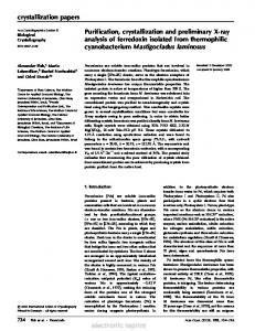
letters to nature Acknowledgements We thank N. Kukhtarev, S. Janz, J. Roovers and I. Le´vesque for stimulating discussions. Correspondence and requests for materials should be addressed to F.dM. (e-mail:
[email protected]) or P.C. (e-mail:
[email protected]).
................................................................. A nanometre-scale electronic switch consisting of a metal cluster and redox-addressable groups David I. Gittins, Donald Bethell, David J. Schiffrin & Richard J. Nichols Centre for Nanoscale Science, Department of Chemistry, University of Liverpool, Liverpool, L69 7ZD, UK .................................. ......................... ......................... ......................... ......................... ........
So-called bottom-up fabrication methods aim to assemble and integrate molecular components exhibiting specific functions into electronic devices that are orders of magnitude smaller than can be fabricated by lithographic techniques. Fundamental to the success of the bottom-up approach is the ability to control electron transport across molecular components. Organic molecules containing redox centres—chemical species whose oxidation number, and hence electronic structure, can be changed reversibly—support resonant tunnelling1,2 and display promising functional behaviour when sandwiched as molecular layers between electrical contacts3,4, but their integration into more complex assemblies remains challenging. For this reason, functionalized metal nanoparticles have attracted much interest5–7: they exhibit single-electron characteristics8–10 (such as quantized capacitance charging) and can be organized11–13 through simple self-assembly methods into well ordered structures, with the nanoparticles at controlled locations. Here we report scanning tunnelling microscopy measurements showing that organic molecules containing redox centres can be used to attach metal nanoparticles to electrode surfaces and so control the electron transport between them. Our system consists of gold nanoclusters
a few nanometres across and functionalized with polymethylene chains that carry a central, reversibly reducible bipyridinium moiety14,15. We expect that the ability to electronically contact metal nanoparticles via redox-active molecules, and to alter profoundly their tunnelling properties by charge injection into these molecules, can form the basis for a range of nanoscale electronic switches. The approach followed in the present work is summarized schematically in Fig. 1. The redox group (‘redox gate’) forms the backbone of a bifunctional ligand that attaches a gold nanoparticle to a gold substrate (see Methods). Electron (or hole) injection to the redox centre is controlled by the potential applied between the substrate and a counter electrode, and the resulting change in barrier transparency can be used to control electron tunnelling between the nanoparticle and the substrate. The tip of a scanning tunnelling microscope (STM) is positioned above the nanoparticle, and is used to monitor electron tunnelling (see Methods). The redox switchable group used here is a bipyridinium (viologen) moiety located at the centre of a chain of 20 methylene units in an a,v-polymethylenedithiol compound (1 in Fig. 1 inset), previously described in refs 14 and 15. Reduction of the bipyridinium group takes place readily and reversibly in a self-assembled film of the ligand on a gold electrode when Au nanoparticles have been attached to the film14,15; the redox process corresponds to the formation of the bipyridinium radical ion:
bipy 2þ þ e 2 O bipy 1þ 2+
ð1Þ 1+
where bipy represents the bipyridinium group and bipy the radical. Scanning tunnelling spectroscopy (STS)16, previously used to study electron transport through individual molecules17 and atoms18, is used to monitor the tunnelling properties of the assembly shown in Fig. 1. In STS, barrier properties are probed by altering the total potential difference between the substrate and the tip (Vbias) and measuring the resulting currents I (see Methods). The STS measurements, which require a constant substrate–tip distance while sweeping the bias voltage and the absence of electrochemical reactions, were conducted in mesitylene by first imaging the area of interest, then placing the tip above the chosen nanoparticle, disabling the feedback loop and immediately measuring the I–Vbias response. Performing this two-terminal measurement in a
Molecule (1) used in redox gate + S
+ N
8
STM tip
N
2 Br
S 8
–
s
Au nanoparticle
6 nm Counter electrode e–
Redox gate
3 nm
Au Substrate Figure 1 Schematic representation of the nanoscopic device. STM was used to examine the electrical characteristics of this device. Electrons can be injected into the redox gate by applying a suitable potential between the substrate and the counter electrode. The potential between the tip and the substrate (Vbias) is controlled independently, and s NATURE | VOL 408 | 2 NOVEMBER 2000 | www.nature.com
represents the tip–nanoparticle distance. The redox gate consists of up to 60 of the molecules shown in the inset. The counter electrode is immersed in the surrounding electrolyte.
© 2000 Macmillan Magazines Ltd
67
letters to nature condensed medium and using a non-polar organic solvent allows the tip–substrate potential difference to be swept over a wide range without interference from electrochemical reactions either on the tip and substrate, or on the redox moiety present in the ligand. In addition, the structures are protected from adventitious contamination. Figure 2 shows an STM image of isolated nanoparticles attached to the bifunctional ligand layer. Figure 3 shows the potential dependence of the current, plotted as (dI/dVbias) in order to highlight the potential dependence of the tunnelling conductivity. The solid line shows the tunnelling conductance of the nanoparticle assembly containing the viologen moieties. A very sharp resonance peak can be seen for tunnelling through the structure. The dashed line corresponds to the control experiment, in which gold nanoparticles were placed over a hexanedithiol monolayer. No peak is seen in the control experiment, showing that the resonance is related to the presence of the redox ligand within the nanoparticle–metal junction. Due to the stability of the bipy1+ state, tunnelling through the junction is likely to occur through a temporary population of the molecular redox state in a two-step electron transfer mechanism. The STS results (Fig. 3) show that the structures investigated display a very marked and sharp resonance with a half-width of 0.2 eV, which favours such a two-step mechanism19. But the STS experiments in mesitylene do not probe changes in barrier characteristics caused by external electron injection, as happens at potentials where the redox group can accept electrons. The advantage of using redox linkers to support nanoparticles is the independent control that can
Figure 2 An STM image of a low coverage of gold nanoparticles deposited on top of a selfassembled monolayer of the redox gate molecule shown in Fig. 1. Current–voltage characteristics (STS), as well as barrier height measurements, were performed by positioning the STM tip over an isolated gold nanoparticle.
be exercised over charge injection to the redox moiety (controlled with respect to a reference electrode in the solution) and the total bias applied between the particle and the substrate. Measurements of inverse decay length16 were used to study the influence of reduction of the bipyridinium group on junction properties. These measurements were conducted in aqueous electrolyte, enabling control of the redox state of the bipyridinium group. After positioning the tip above a chosen nanoparticle, the feedback loop was switched off, the tip was advanced 0.2 nm towards the surface and the current measured as the tip was withdrawn back to its original position at a rate of 2.2 nm s−1. From the average of several I(s) measurements (where s is the distance between the tip and the particle), the inverse decay length was calculated from the distance dependence of d(ln I)/ds according to16: d lnI t ¼ 2 2k ð2Þ ds where 2k is the inverse decay length of the tunnelling current. k is a measure of the decay of the electronic wavefunction away from the sample surface, as probed by the STM tip. The inverse decay length drops sharply on reduction of bipy2+ to bipy1+, from 16 6 1 nm−1 for bipy2+ to 7 6 1 nm−1 for bipy1+. Previous electrochemical STS experiments20 on Au(111) surfaces (also replicated by us, results not shown) indicate that the inverse decay length does not alter markedly with electrode potential: the changes observed here are due to the injection of charge into the redox group, and not to changes in the electrical double layer. Our measurements of the inverse decay length reflect the changes in the electronic properties of the junction brought about by redox switching. When the redox group in the junction is reduced, the electronic wavefunction of the gold surface, the bipy1+ moiety and the nanoparticle extensively couple, leading to conductivity in the junction. We propose that the dramatic change in the nature of the barrier when the bipyridinium group is reduced gives rise to the large change observed in the tunnelling parameters. These observations are currently being considered within the theoretical framework of the mechanism of electron tunnelling (J. Ulstrup, personal communication). In Fig. 4 we show the operation of a molecular switch based on the results we report here. By controlling the substrate-to-solution potential, the bipyridinium group can be switched between its oxidized (bipy2+) and reduced (bipy1+ and bipy0) states. With the bipyridinium in its bipy1+ reduced state (Fig. 4, centre panel), the device shows a high barrier transparency resulting from the
S Current (nA)
dI/dV (nA V–1)
30
20
S
π
T
–2 0 Substrate bias (V)
10
R
–2.0
T
S
0
0 –1.5 –1.0 –0.5 Substrate bias (V)
0.0
Figure 3 A current–voltage curve (inset) and its derivative (dI/dVbias) obtained for the surface shown in Fig. 2, immersed in mesitylene. The STM tip was positioned above an isolated gold nanoparticle for these measurements. The dotted line corresponds to the control experiment, in which gold nanoparticles were deposited on a hexanedithiol monolayer. 68
T
π*
5
+ N
+ N
R
R
N
+ N R
R
N
N
R
Figure 4 A schematic illustration of the operation of a nanoscopic electronic switch illustrated in Fig. 1. The figure shows the energy levels corresponding to the conduction bands of the substrate and STM tip (S, gold substrate; T, STM tip), and the lowest unoccupied molecular orbital and highest occupied molecular orbital of the bipyridinium moiety. Three redox states are shown: bipy2+ (left), bipy1+ (middle) and bipy0 (right). When the redox gate molecule is in its bipy1+ reduced state (centre), the device shows a high barrier transparency.
© 2000 Macmillan Magazines Ltd
NATURE | VOL 408 | 2 NOVEMBER 2000 | www.nature.com
letters to nature extension of the electronic wavefunction from the gold surface through the bipy1+ group and the nanoparticle. The resulting increase in conductivity provides the basis for the operation of this low-voltage switching structure. The bipyridinium group has a footprint of approximately 0.45 nm2 (ref. 21), and a maximum of 60 redox ligands could be attached to each gold nanoparticle. The actual number is most likely to be much less than this owing to steric hindrance by the chains, and we expect that the switch requires less than 30 electrons to operate (with half of the redox ligands in their reduced state). M
22. Brust, M., Bethell, D., Schiffrin, D. J. & Kiely, C. J. Novel gold-dithiol nano-networks with nonmetallic electronic properties. Adv. Mater. 7, 795–797 (1995). 23. Bethell, D., Brust, M., Schiffrin, D. J. & Kiely, C. From monolayers to nanostructured materials - an organic chemist’s view of self-assembly. J. Electroanal. Chem. 409, 137–143 (1996). 24. Ulman, A. An Introduction to Ultrathin Organic Films (Academic, San Diego, 1991).
Acknowledgements This work was supported by the UK EPSRC Scanning Probe Microscopy initiative. D.I.G thanks EPRSC for the award of a quota studentship. D.B. thanks the Leverhume Trust for the award of an Emeratus Fellowship. Correspondence and requests for materials should be addressed to R.J.N. (e-mail:
[email protected]).
Methods Preparation of nanostructures The preparation of N,N-di-(10-mercaptodecyl)-4,49-bipyridinium dibromide (1 in Fig. 1)14 and solutions of gold nanoparticles have been described previously22,23. The gold on glass substrates were cleaned in 70:30 H2SO4:H2O2 (after use this solution must not be stored as explosive oxo-peroxides may form), and annealed using a high-purity hydrogen/ air flame to yield Au(111) surfaces. Au film electrodes were derivatized by immersion for 18 h in 1 mM methanol solutions of (1)24, washed with methanol and toluene, and then immersed in a toluene solution of gold nanoparticles (average size 6 nm) for a short time so as to attach well-separated particles on the surface.
STM/STS measurements These were performed with a Pico2000 system (Molecular Imaging) using PicoScan software. STM tips (0.25 mm diameter 80:20 Pt-Ir wire, Goodfellow) were mechanically sharpened on a polishing wheel using fine abrasive paper. The STS measurements were performed using uncoated Pt-Ir tips in mesitylene, and two-probe measurements were made by altering the potential difference between the substrate and tip (Vbias), as described in ref. 2. In contrast, the inverse decay length measurements were recorded in aqueous electrolytes (0.1 M potassium phosphate buffer, pH 7) under N2, and Vbias and the electrode potential were controlled independently using a bipotentiostat. For these experiments, the Pt-Ir STM tips were freshly coated with a layer of Apiezon wax before use to decrease leakage currents (these were measured at a tip bias of 200 mVand only tips with a leakage current lower than 5 pA were used). The microscope was operated in a constantcurrent mode with a tunnelling current of 50 pA and 200 mV bias (tip positive). Scans in both directions (away and towards the substrate) were recorded to ensure that the tip– sample interactions were not perturbing the results. All solutions were de-aerated with high purity nitrogen for 20 min before use. Received 6 April; accepted 24 August 2000. 1. Tao, N. J. Probing potential-tuned resonant tunneling through redox molecules with scanning tunneling microscopy. Phys. Rev. Lett. 76, 4066–4069 (1996). 2. Han, W. H. et al. STM contrast, electron-transfer chemistry, and conduction in molecules. J. Phys. Chem. B 101, 10719–10725 (1997). 3. Feldheim, D. L. & Keating, C. D. Self-assembly of single electron transistors and related devices. Chem. Soc. Rev. 27, 1–12 (1998). 4. Chen, J., Reed, M. A., Rawlett, A. M. & Tour, J. M. Large on-off ratios and negative differential resistance in a molecular electronic device. Science 286, 1550–1552 (1999). 5. Ashoori, R. C. Electrons in artificial atoms. Nature 379, 413–419 (1996). 6. Collier, C. P., Saykally, R. J., Shiang, J. J., Henrichs, S. E. & Heath, J. R. Reversible tuning of silver quantum dot monolayers through the metal-insulator transition. Science 277, 1978–1981 (1997). 7. Oosterkamp, T. H. et al. Microwave spectroscopy of a quantum-dot molecule. Nature 395, 873–876 (1998). 8. Chen, S. W. & Murray, R. W. Electrochemical quantized capacitance charging of surface ensembles of gold nanoparticles. J. Phys. Chem. B 103, 9996–10000 (1999). 9. Ingram, R. S. et al. 28 kDa alkanethiolate protected Au clusters give analogous solution electrochemistry and STM coloumb staircases. J. Am. Chem. Soc. 119, 9279–9280 (1997). 10. Andres, R. P. et al. ‘‘Coulomb staircase’’ at room temperature in a self-assembled molecular nanostructure. Science 272, 1323–1325 (1996). 11. Kiely, C. J., Fink, J., Brust, M., Bethell, D. & Schiffrin, D. J. Spontaneous ordering of bimodal ensembles of nanoscopic gold clusters. Nature 396, 444–446 (1998). 12. Schmid, G. Clusters and Colloids (VCH, Weinheim, 1994). 13. Templeton, A. C., Wuelfing, M. P. & Murray, R. W. Monolayer protected cluster molecules. Acc. Chem. Res. 33, 27–36 (2000). 14. Gittins, D. I., Bethell, D., Nichols, R. J. & Schiffrin, D. J. Diode-like electron transfer across nanostructured films containing a redox ligand. J. Mater. Chem. 10, 79–83 (2000). 15. Gittins, D. I., Bethell, D., Nichols, R. J. & Schiffrin, D. J. Redox-connected multilayers of discrete gold particles: A novel electroactive nanomaterial. Adv. Mater. 11, 737–740 (1999). 16. Chen, C. J. Introduction to Scanning Tunneling Microscopy (Oxford Univ. Press, New York, 1993). 17. Joachim, C., Gimzewski, J. K., Schlittler, R. R. & Chavy, C. Electronic transparency of a single C60 molecule. Phys. Rev. Lett. 74, 2102–2105 (1995). 18. Yazdani, A., Eigler, D. M. & Lang, N. D. Off-resonance conduction through atomic wires. Science 272, 1921–1924 (1996). 19. Friis, E. P. et al. An approach to long-range electron transfer mechanisms in metalloproteins: In situ scanning tunneling microscopy with submolecular resolution. Proc. Natl Acad. Sci. USA 96, 1379– 1384 (1999). 20. Vaught, A., Jing, T. W. & Lindsay, S. M. Non-exponential tunneling in water near an electrode. Chem. Phys. Lett. 236, 306–310 (1995). 21. DeLong, H. C. & Buttry, D. A. Environmental effects on redox potentials of viologen groups embedded in an electroactive SAM. Langmuir 8, 2491–2496 (1992).
NATURE | VOL 408 | 2 NOVEMBER 2000 | www.nature.com
................................................................. Large disparity between gallium and antimony self-diffusion in gallium antimonide H. Bracht*†, S. P. Nicols*, W. Walukiewicz*, J. P. Silveira‡, F. Briones‡ & E. E. Haller* * University of California and Lawrence Berkeley National Laboratory, Berkeley, California 94720, USA ‡ Instituto de Microelectro´nica de Madrid, Centro Nacional de Microelectro´nica, CSIC, Serrano 144, 28066 Madrid, Spain .......................................... ......................... ......................... ......................... .........................
The most fundamental mass transport process in solids is selfdiffusion. The motion of host-lattice (‘self-’) atoms in solids is mediated by point defects such as vacancies or interstitial atoms, whose formation and migration enthalpies determine the kinetics of this thermally activated process1,2. Self-diffusion studies also contribute to the understanding of the diffusion of impurities, and a quantitative understanding of self- and foreign-atom diffusion in semiconductors is central to the development of advanced electronic devices. In the past few years, self-diffusion studies have been performed successfully with isotopically controlled semiconductor heterostructures of germanium3, silicon4, gallium arsenide5,6 and gallium phosphide7. Self-diffusion studies with isotopically controlled GaAs and GaP have been restricted to Ga self-diffusion, as only Ga has two stable isotopes, 69Ga and 71Ga. Here we report self-diffusion studies with an isotopically controlled multilayer structure of crystalline GaSb. Two stable isotopes exist for both Ga and Sb, allowing the simultaneous study of diffusion on both sublattices. Our experiments show that near the melting temperature, Ga diffuses more rapidly than Sb by over three orders of magnitude. This surprisingly large difference in atomic mobility requires a physical explanation going beyond standard diffusion models. Combining our data for Ga and Sb diffusion with related results for foreign-atom diffusion in GaSb (refs 8, 9), we conclude that the unusually slow Sb diffusion in GaSb is a consequence of reactions between defects on the Ga and Sb sublattices, which suppress the defects that are required for Sb diffusion. Compared to conventional self-diffusion experiments, which use radioactive probe atoms of the matrix introduced from the surface, diffusion studies with highly enriched stable isotopes are neither limited by the half-life of the radiotracer nor affected by nearsurface degradation. Such diffusion experiments can therefore be extended to much longer times and conducted over a wider temperature range. In combination, these advantages lead to more accurate data for the activation enthalpy of self-diffusion. †Present address: University of Mu¨nster, Institut fu¨r Materialphysik, Wilhelm-Klemm-Strasse 10, D-48149 Mu¨nster, Germany.
© 2000 Macmillan Magazines Ltd
69