A New Voltage-balancing Controller in Cascaded Multilevel Converters Xu She, Student Member, IEEE, Alex Q.Huang, Fellow, IEEE, Gangyao Wang, Student Member, IEEE, Tiefu Zhao, Member, IEEE, Fei Wang, and Wenxi Yao
Abstract—Voltage-balancing controller in cascaded multilevel converters has been discussed extensively in previous literatures where several effective methods have been proposed. The coupling effect between a voltage-balancing controller and the original system controller is however not addressed comprehensively. This paper proposes a new voltage-balancing controller for single-phase cascaded multilevel converters in a dq coordinate. The theoretical finding shows that the proposed method can effectively eliminate the coupling between two controllers in both steady and dynamic state. Simulation and experimental results validate the proposed method. Index Terms—cascaded multilevel converter, voltage balance, d-q control, decouple control
I. INTRODUCTION
T
HE multilevel converters are appealing solutions for high voltage applications since it is generally difficult to utilize a single power semiconductor to switch directly [1]. Cascaded multilevel converters have gained considerable attention recently compared with other multilevel topologies due to its advantages in terms of modularization, extendibility, and minimization of power semiconductors [1]-[28]. It has been proposed and widely employed in high voltage and high power applications such as inverters in AC motor drives, static synchronous compensators (STATCOM), and active power filters (APF) [4]-[9]. Another attractive application is to use this topology as a bidirectional active rectifier because of the available distinct dc links feeding separate loads [10]. It can reduce the harmonic distortion at the AC side and provide satisfactory regulation for all DC links. A good application example is the solid-state transformer (SST), which is reported in [11]. DC capacitor voltage imbalance is an inherent problem for both multilevel converter systems and multi-pulse converter systems [12]-[13]. In a cascaded multilevel converter, this can be caused by mismatch of active and passive components, different switching pattern, control resolutions, and different loads (operating as a rectifier) [7], [10]. The imbalance of the DC capacitor voltage will lead to degradation of the input current, imbalance of loss in each H-
This work was supported National Science Foundation under Award EEC0812121. Xu She, Alex Q.Huang, Gangyao Wang, and Fei Wangare with Future Renewable Electric Energy Delivery and Management Systems Center, North Carolina State University, Raleigh, NC 27695, USA (e-mail:
[email protected],
[email protected],
[email protected],
[email protected]). Tiefu Zhao is with Eaton Corporation, 4201 North 27th street, Milwaukee, WI 53261, USA (
[email protected]) Wenxi Yao is with Zhejiang University, Hangzhou, ZJ 310027, China (email:
[email protected])
978-1-4577-0541-0/11/$26.00 ©2011 IEEE
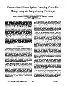
bridge, and even collapse of the whole system (over voltage, over current, etc) [14]. The basic requirement for a DC voltage-balancing controller is to balance the DC link voltages under all operation conditions. While a good DC voltagebalancing controller should also be simple, fast, and easily expanded to a cascaded converter with N H-bridges. Besides, the reactive power should be controlled independently of the active power, thus it can be possibly equally distributed in each H-bridge cell according to the requirement. Furthermore, the voltage-balancing controller should couple with the original system controller as less as possible. The last point emphasized here requires for a control system that can be separated into two decoupled layers. The upper layer only control the total DC voltage and the lower layer only eliminate the voltage difference among H-bridges. In this paper, a new voltage-balancing controller is proposed to reduce the coupling effect between the voltagebalancing controller and the original system controller for a single-phase cascaded multilevel converter. A single-phase dq model is firstly established with consideration of DC voltage imbalance. Then the coupling term between two controllers is identified and a control scheme is proposed to eliminate it. Comparisons between the proposed method and previous methods are conducted. Furthermore, DC voltage-balancing controller reference generation techniques are discussed and proved to be of big impact to the DC voltage balance during the start up process. A suitable reference is then chosen to get rid of this undesired impact. Simulations and experiments are provided to validate the theoretical findings. II. AVERAGE MODELING IN D-Q COORDINATE CONSIDERING VOLTAGE IMBALANCE Fig.1 (a) shows the configuration for a single-phase cascaded multilevel rectifier with N H-bridges. vs is the point of common
coupling
(PCC)
voltage,
Ls is
the
boost
inductor, Rs is the equivalent resistor of the inductor ,wire, and losses. Ci and Ri ( i = 1...N ) are DC capacitors and loads in each DC output. N H-bridges are series connected to synthesize a 2N+1 level waveform, which is vab , from N isolated DC voltage sources, which are denoted as vdc1 − vdcN . Taij (i = 1...N , j = 1...4) denotes the switches in the
converter.
177
Rs
Ta13
is
Ls
The average modeling in d-q coordinate considering the voltage imbalance can be obtained as:
idc1
Ta11
vab1
C1
Ta12
Ta14
Ta 21
Ta 23
⎡ d ⎤ ⎛ − Rs ⎢ dt isd ⎥ ⎜ Ls ⎢ ⎥ =⎜ ⎢ d i ⎥ ⎜ −w ⎢⎣ dt sq ⎥⎦ ⎜ ⎝
R1
vdc1 idc 2
vs
vab 2
vab
Ta 24
TaN 1
TaN 3
vdc 2
idcN
vabN TaN 2
CN
vdcN
TaN 4
(a) Topology of original N H-bridges cascaded rectifier idc1 Ta11 Rs
Ls
Tm11
Tm13
is
Ls
vab1 Ta12
Ta 21
vs
Ta13
vab
C1
Tm12
Tm14
Tm 21
Tm 23
Tm 24
Tm 22
TmN 1
TmN 3
TmN 2
TmN 4
idc 2
Ta 23
vab 2 Ta 22
Ta 24
TaN 1
TaN 3
C2
vdc 2
vm
R2
idcN
vabN TaN 2
TaN 4
CN
vdcN
RN
(b) Topology of N H-bridges cascaded rectifier with hypothesized phase Fig. 1 Topology for cascaded rectifier with N H-bridges
Different from the three-phase system, N imaginary Hbridges, which lag 900 with the original N H-bridges, have to be hypothesized in order to realize the single-phase d-q transformation [29]. This is illustrated in Fig. 1 (b). The inductor current in the real and hypothesized cascaded Hbridges are represented as is and im while the PCC voltage for the hypothesized converter is vm . Tmij (i = 1...N , j = 1...4) denotes the switches in the hypothesized converter. The relationship between vs and vm is shown in Fig. 2. The detailed theory of the single-phase d-q transformation can be found in [29].
vs vm 900
⎡ d dN ⎤ ⎢d ⎥) ⎣ qN ⎦
I base is the base value of the input current. H ed , H id , H iq are
im
R1
vdc1
Ta14
Rs
⎡dd 2 ⎤ vdcN ⎢ d ⎥ + ... + Ls ⎣ q2 ⎦
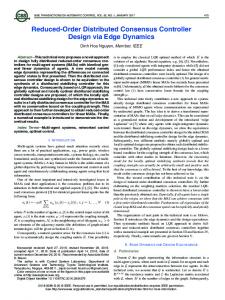
(1) d vdci vdci (i = 1...N ) d di isd + d qi isq = Ci + (2) dt Ri In the cascaded multilevel inverter application, the reactive current is controlled to a certain value for reactive power compensation (such as in STATCOM and APF). In the active rectifier application, the reactive current is controlled to zero to obtain unity power factor. The DC capacitor voltage is regulated by the active current. Fig. 3 demonstrates the d-q coordinate dual loop control for a cascaded multilevel rectifier with N H-bridges. In Fig. 3, NE is the total DC voltage reference, Vbase is the base value of the PCC voltage, and
C2
Ta 22
⎞ w ⎟ ⎡i ⎤ ⎡ v ⎤ d ⎟ ⎢ sd ⎥ + ⎢ sd ⎥ 1 − ( vdc1 ⎡⎢ d 1 ⎤⎥ + vdc 2 d − Rs ⎟ ⎢isq ⎥ ⎢ vsq ⎥ Ls L Ls s ⎣ q1 ⎦ ⎟⎣ ⎦ ⎣ ⎦ Ls ⎠
the controllers for the DC bus voltage, active current, and reactive current respectively. The dq-am transformation and the d-q decoupling control can be found in [29], which is similar with the classical d-q decoupling control in a threephase system. PCC voltage feed-forward control is also implemented so that the distortion of the grid voltage will not affect the controller since only the L-type filter is adopted in this paper. In the DC voltage loop, a notch filter at 120Hz is added to the feedback loop to eliminate the second harmonic component in the DC capacitor voltages by assuming that the grid frequency is 60Hz. If the controller only considers the DC capacitor voltages balanced condition and only controls the total DC voltages, it is called the original system controller in this paper. If the system is unbalanced, certain modification has to be made for active component of duty cycles, which are Δd1 , Δd 2 , … Δd n , as shown in dotted arrow, and these are given by an additional voltage balancing controller. Since the total DC voltage is already regulated by the original system controller, only N-1 additional DC voltage control loop can be added. If the duty modification of the last one is not well designed, this additional voltage-balancing controller is coupled with original system controller. The effort of this paper is to minimize the coupling effect between the original system controller and the voltage balancing controller as such they can be designed separately. III. A NEW VOLTAGE BALANCING CONTROLLER WITH MINIMUM EFFECT TO THE ORIGINAL CONTROLLER A. Theoretical Analysis DC voltage in each capacitor may become imbalanced for many reasons such as different loads connected to each DC port. Although the total voltage is still controlled by the original system controller, the unequal distribution of voltage among H-bridges exists. Active power should be re-distributed among H-bridge modules in order to achieve voltage balance.
Fig. 2 Relationship between values in real and hypothesized circuits
178
vs
vsd
θ
1 / V sb ase
vm
vdc1 vdc 2
+
+
1/ NE +
vdcN
−
+ 1
is
isd
1/ I sbase
vsq
isq
θ
H ed
vsd
isdref +
isd isq
−+ +
H id
−
dd
wLs / NE
+
wLs / NE
−
−
H iq
isqref
−
dq
Δd1 +
+
Δd 2 +
+
Δd N +
+
d a1 da 2
d aN
vsq
+
Fig. 3 D-q coordinate controller for N H-bridges cascaded multilevel converter
The dynamic equation for the original system controller can be described by (3), where d d and d q are active and
the pre-designed original system controller. Define the coupling index as follows:
reactive duty cycle generated by it. The average voltage of each DC output is assumed to be E , which should be selected as the reference for the DC voltage balance controller as shown in (4). This will be further explained in detail in part IV. di Ls sd = − Rs isd + wLs isq + vsd − N Ed d dt (3) disq = − Rs isq − wLs isd + vsq − N Ed q Ls dt
J1 = ( N Ed d − ∑ d di vdci ) 2 = ( N Ed d − ∑ (d d + Δdi )( E − Δvdci )) 2
2
(8)
i =1
Where, Δdi is the modification of duty cycle and Δvdci is the error between the reference and the feedback voltage for each DC output. Since the reactive duty cycle are not modified and this means d q = d qi . (8) is already zero since E is chosen as
(4)
shown in (4). The problem of how to minimize J1 can be achieved if equation (9) is satisfied. N
∑ (d
d
+ Δdi )( E − Δvdci ) = N Ed d
(9)
i =1
Expand (5) further leads to:
the modified duty cycles. The dynamic equation for the system becomes: N di Ls sd = − Rs isd + wLs isq + vsd − ∑ vdci d di dt i =1 (5) N disq = − Rs isq − wLs isd + vsq − ∑ vdci d qi Ls dt i =1 This can be rewritten as: N di Ls sd = − Rs isd + wLs isq + vsd − N Ed d + ( N Ed d − ∑ vdci d di ) dt i =1 (6) N disq Ls = − Rs isq − wLs isd + vsq − N Ed q + ( N Ed q − ∑ vdci d qi ) dt i =1 Comparing equation (6) with (3), it is clear that i =1
i =1
J 2 = ( N Ed q − ∑ d qi vdci )
When DC voltages become imbalanced, voltages in DC ports are denoted as vdci (i = 1...N ) and d di , d qi (i = 1...N ) are
N
i =1
(7)
i =1
( N Ed d − ∑ vdci d di )
N
N
N
N E = ∑ vdci
N
N
∑d i =1
d
N
N
N
i =1
i =1
i =1
E − ∑ d d Δvdci + ∑ Δdi E − ∑ Δdi Δvdci = N Ed d
(10)
Equation (10) can be simplified as: N
∑ ( E − Δv
dci
i =1
N
N
i =1
i =1
)Δdi = ∑ (vdci )Δdi = ∑ Δvdci d d
(11)
Since there are altogether N DC voltages needed to be controlled and the total DC voltage has already been regulated by the original system controller, only N-1 closed loop regulator can be added in order to ensure the stability of the control system. Without losing generality, the modifications of duty cycles for the first N-1 H-bridges are generated by a PI controller, thus to eliminate the difference between the feedback value and the reference value. Δdi = k pi (vdcref − vdci ) + kii ∫ (vdcref − vdci )(i = 1...N − 1) (12)
N
and ( N Ed q − ∑ vdci d qi ) are the additional terms i =1
Then the modification of active duty cycle in Nth H-bridge should meet (13) in order to minimize the coupling effect.
added by the voltage balancing controller. If an advanced modulation strategy is adopted, these two terms will be zero since duty cycles are not modified. However if feedback closed loop regulation is adopted, duty cycle is modified for each H-bridge thus making the first term unequal to zero. The key strategy in this paper is to eliminate this additional term so that the voltage-balancing controller will not affect
N
∑ Δv
dci
Δd N =
179
i =1
N −1
d d − ∑ vdci Δdi i =1
vdcN
(13)
If the total DC voltage is controlled properly, which means the voltage difference comes out among H-bridges while the total DC bus voltage is controlled well, then the following approximation is reasonable: N
∑ Δv
dci
≈0
N
∑ Δd
(14)
Then the following approximation equation for (13) is satisfied:
N −1
Δ d N = − ∑ Δd i
−∑ vdci Δdi i =1
vdc1
vdc 2 ref
. . vdcN −1 − vdc ( N −1) ref. +
H edc1 H edc 2
H edcN −1
Δd1
Δd 2
N
Δd N −1
∑ Δd
. vdcN −1 . .
+
-1 −
vdcN
÷
Δd N
N
i =1
is obvious that the lower the coupling index is, the better the performance is. The comparison is made between the proposed method and the method in [20], [27], and [28]. In the comparison, three H-bridges are cascaded to a seven-level converter. The input AC voltage is 110 V and the DC voltages are set to 70 V for each port, which has 25 Ω load connected to it. The inductor is chosen to be 3.5 mH , and capacitor is chosen as 900 μF .
: multiplier dd
B. Comparison of proposed methods with previous methods In order to compare the proposed method with the previous methods proposed in [25]-[28], which all try to balance the DC bus voltage in the d-q coordinate. The equivalent duty cycle modification expressions in these literatures are analyzed below. (1) Method proposed in [25]-[26] The methods proposed in [25] and [26] are based on the per-phase modification concept, and the modifications of duty cycles are defined in (16). This method is theoretically not suitable since it has together N+1 voltage loops to control N DC voltages, thus may bring oscillation in the system. Δdi = k pi (vdcref − vdci ) + kii ∫ (vdcref − vdci )(i = 1...N ) (16)
N
Fig. 5 demonstrates the value of ( N Ed d − ∑ vdci d di )2 for both i =1
cases when there is a voltage imbalance caused by load change at 2 s . In this scenario, the load connected to the third H-bridge is changed from 25 Ω to 35 Ω . The red one is the coupling index by adopting the proposed method, and the blue one is the one by adopting the method equivalent to the one proposed in [20],[27], and[28]. It can be observed that before the load disturbance, both values approximate to zero. Unlike the proposed method, in which the value is still zero when voltage becomes imbalanced, the value becomes large when imbalance happens and it will decrease as the voltage becomes balanced by using the methods proposed in [20], [27],and [28].Obviously, the previously proposed methods will bring an additional term to the original system dynamics when the system is imbalanced, and this can be eliminated by the proposed method. Besides, the coupling interaction becomes worse when the voltage imbalance is serious. The wider the range of load changes, the larger the effect of the additional term to the original system dynamic becomes. The
(2) Method proposed in [27] The method adopted in [27], which is the same with the one used in [20], is shown in (17). The idea is to distribute the duty cycle to each H-bridge so that the total power transferred is guaranteed. The relationship among modifications of duty cycles are satisfied as shown in (18).
ki = k pi (vdcref − vdci ) + kii ∫ (vdcref − vdci )(i = 1...N ) ki
(17)
N
∑k
(20)
Take the coupling index ( N Ed d − ∑ vdci d di )2 as the criterion, it
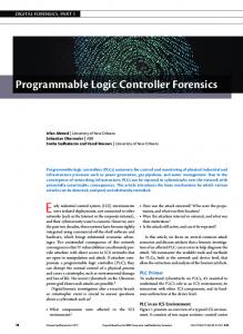
Fig. 4 Voltage balance controller for cascaded H-bridge converter
d di = d d
=0
The difference between the proposed method and the previous methods is that it considers the actual DC voltages when designing the voltage-balancing controller. If assuming that the system has operated in a steady state after the load disturbance, which means the DC bus voltages have converged to the same value, (13) and (15) proposed in this paper are the same with (18) and (20). However, when the cascaded converter is operating as a rectifier with load on each DC port, power in each DC port always changes. Therefore, the DC bus voltage is always in a dynamic state. During these dynamic responses, the DC voltages are actually imbalanced. The addition of the voltage-balancing controller will affect the original system controller dynamics.
: adder
+ + +
+ +
i
i =1
vdc1
vdc 2
(19)
i =1
(15)
vdcN The proposed voltage-balancing controller is shown in Fig. 4, where H edci (i = 1...N − 1) are PI controllers for the first N-1 H-bridges. It should be noted that (13) provides the fundamental relationship among modification values of active duty cycles for all H-bridges, which is especially important and differs with previous methods especially when DC capacitor voltages are not exactly the same. If the total DC voltage is controlled well, (15) can be adopted as a good approximation, as shown in the dotted line in Fig. 4. − + vdc 2 − +
(18)
Δdi = k pi (vdcref − vdci ) + kii ∫ (vdcref − vdci )(i = 1...N − 1)
N −1
vdc1ref
=0
(3) Method proposed in [28] The method proposed in [28] is actually the same with the method in [27], as illustrated in (19) The summation of the duty modification equals to zero.
i =1
Δd N =
i
i =1
i
consequence of the term
i =1
N
( N Ed d − ∑ vdci d di )
may lead to an
i =1
unexpected
180
performance
of
the
pre-designed
system
controller, and this unpredicted effect may be unacceptable. The purpose of the proposed decoupling method is to eliminate this effect so that the two controllers can be designed separately with the desired performance. 3
P1 N
∑ Pi
≤
wL I E 1 − ( s s )2 Vs NE
(27)
i =1
As shown in (27), the balancing operation of the system is limited by the active power distribution of it. Equation (27) is a good estimation for the power difference allowed for the designed system.
Proposed controller Previous controller
2
1
0
D. Experimental Results The validity of the proposed method is verified in a three H-bridges cascaded seven-level active rectifier through experimental work. The system parameters are set in Table. I. The switch adopted is the INFINEON 20N60CFD power MOSFET. Two 25 mH inductors (ferrite core with air gap) are connected in series to compose the desired 50 mH input filter inductor. Since the experiments are carried out in a low frequency and very low current situation [11], the input inductance is chosen to be relatively large. However this will not affect the performance evaluation. Two 100 μF , 200 V capacitors produced by Nichicon are paralleled in each DC output. The controller is realized by using the TI TMS320F 28335 DSP. In the experiments, the input AC voltage is generated from Chroma AC power supply (61602) and three variable resistance load banks are used as the loads.
-1
-2
-3 0
0.5
1
1.5
2
2.5
3
3.5
4
Fig. 5 Comparison of coupling index between proposed method and previous methods
C. Discussion of on voltage balancing controller effective range issue The proposed control system contains an original system controller and N-1 voltage-balancing controllers. The PI tuning process should follow certain principles. The original system controller should be designed firstly by assuming that there is no voltage imbalance exists. The design of this controller is the same with a traditional boost rectifier dual loop control system [10]. The output of voltage balancing controller is added to the original system controller output as the modification, so the effective voltage balancing area should be defined, which is mainly limited by the modulation index. Finally, the N-1 DC voltage-balancing controllers can be designed within the preset PI output limitation according to the real operation conditions. The PI parameter tuning is not the key in this paper and is not discussed in detail. The voltage-balancing constraint can be derived as shown below [28]. According to the circuit shown in Fig. 1: N
∑V
= Vs − jwLs I s
(21)
Vabi = (d di + d qi j ) E (i = 1...N )
(22)
abi
Table. I system parameter Source voltage
80Vrms
Source frequency
60Hz
DC link voltage
i =1
Substitute (22) into (21) and rearrange the terms: N V (23) d di = s ∑ E i =1 N − wLs I s (24) d qi = ∑ E i =1 The active power of each H-bridge can be calculated as: P (25) Pi = I s d di E = in d di E (i = 1...N ) Vs When loads connected to DC ports are different, the active power consumed by them is different. Without losing generality, assume that d d 1 ≥ d d 2 ≥ ... ≥ d dN . For each Hbridge, the operation is limited by the modulation index: d di2 + d qi2 ≤ 1(i = 1...N ) (26) Substitute (25) into (26) and assume that the reactive power is equally distributed among H-bridges, the following constraints for active power distribution is obtained:
50*3 = 150V
Switching frequency
1080Hz
Input inductance
50mH
DC link capacitor
200uF
DC load resistor
250Ω
(a) Balanced state DC voltages
(b) Balanced state AC side waveforms
181
difference. In the Fig. 6 (d), the DC voltages can converge to 50 V immediately with the aid of the proposed voltagebalancing controller. Considering that the modification mechanism of the duty cycle for the third H-bridge is different from the first and the second H-bridge, a test is also conducted for the third H-bridge to verify the effectiveness of the proposed controller. In Fig. 6 (e), without the voltagebalancing controller, Vdc 3 becomes lower than 50 V and Vdc1 , Vdc 2 becomes higher than 50 V when R3 changes from 250 Ω to 220 Ω . While in Fig. 6 (f), the voltages converge to 50 V immediately after the loads change due to the effectiveness of the proposed voltage-balancing controller. It can be concluded from Fig. 6 that the proposed voltage-balancing controller can effectively balance the DC voltages.
(c) Voltage imbalance in H-bridge 2
IV. INVESTIGATION ON REFERENCE GENERATION TECHNIQUES OF VOLTAGE BALANCING CONTROLLER
(d) Voltage balancing process in H-bridge 2
In part III, the relationship among modification of duty cycles in H-bridges is analyzed. Another important, yet easily ignored problem is how to design the reference generation for the balancing controller. In the previous literature, a discussion of the effect of the balancing controller to soft start-up process is rare. In the following analysis, the effect of the reference generation to the start-up process is identified and addressed. In previous PI-based control algorithms, the reference of the balance-controller is not mentioned [20]-[23] or is given by a fixed value that is equal to the steady state value [10],[19],[25],[28]. In industrial applications, a soft start-up process is needed especially for a high power and high voltage converter, in which huge inrush current may damage the power semiconductor devices. Fig. 7 shows the typical DC bus voltage of a rectifier using a soft start algorithm. The system is firstly charged through a resistor connected between PCC and the cascaded H-bridges to avoid a large inrush current. Then the resistor is bypassed and a diode charge is performed to charge the DC capacitor voltage. When the diode charge is finished, a ramp current charge is used with only the current loop regulation to further charge the DC capacitor voltage and approach the rated value. Lastly, the DC outer loop is closed to realize the steady state regulation.
(e) Voltage imbalance in H-bridge 3
(f) Voltage balancing process in H-bridge 3 Fig. 6 Experimental results of cascaded seven-level converter
Fig. 6 shows the experimental results of the proposed method and are explained as follows. Fig. 6 (a) shows the balanced DC voltages when the load connected to each output are equal. The DC voltages are all controlled to 50 V . Fig. 6 (b) shows the AC voltage, PWM voltage, and AC current under this situation. Since the converter is cascaded by three H-bridges under the PS-PWM [30], it generates a seven-level PWM voltage. The input current is in phase with the input voltage thus indicates a unity power factor. In order to verify the effectiveness of the proposed voltage-balancing controller, the comparison is made between the dynamic response of DC voltages without the voltage-balancing controller and with the voltage-balancing controller when load R2 changes from 250 Ω to 220 Ω . Fig. 6 (c) shows the DC voltages without the voltage-balancing controller. The voltages diverge to different values because of the load
Vc
(1)
(2)
(3)
(4)
Fig. 7 Soft-start algorithm of rectifier
182
vs
vsd
θ
1 / V sb a se
is
isd
1/ I sbase
vsq
isq
vm
θ
vdc1 vdc 2
+
+
1/ NE
−
+ 1
+
vdcN
H ed
vsd
isdref +
isd
H id
−
+
wLs / NE
−
H iq
isqref
+
−
vdc 2 − +
vdcN −1 +
H edc1 H edc 2
−
H edcN
Δd1
Δd 2
Δd N −1
dd
wLs / NE
isq
vdc1
− + +
−
−
dq
Δd1
+
d a1
+ Δd 2 +
da2
Δd N + +
d aN
+
+ vsq
vdc1
vdc 2 vdcN −1
+ +
+ −
vdcN
÷
Δd N
+ + +
dd
Fig. 8 Control diagram of cascaded rectifier under d-q coordinate
It is understood that when the system works under the softstart process, the total DC capacitor voltage is below the desired voltage. If the reference value for the balancing controller remains constant, even if the voltages are balanced, there will still be a modification value generated by the voltage-balancing controller, which may lead to undesired DC bus regulation performance. In order to eliminate this phenomenon, this paper recommends the average DC bus voltage of all H-bridges as the reference voltage for DC voltage-balancing controller. By adopting this method, the DC capacitor voltage will be balanced during the start-up process since the reference is changing with the actual DC bus voltage, then the effect of the voltage-balancing controller to the original system controller will be further minimized and two controllers are totally decoupled. Based on what has been discussed above, the whole control system is given in Fig. 8, and the voltage-balancing controller is based on (13). The whole system controller is divided into two layers. The upper layer is the original system controller and the lower layer is the voltage-balancing controller. In order to compare the performance of the presented reference generation method with traditional ones in [10],[19],[25] and [28], a soft-start performance is carried out for three cases under balanced load condition, and the waveforms are given in Fig. 9.
(b) DC voltages with balanced load with traditional voltage reference generation
(c) DC voltages with balanced load with presented voltage reference generation Fig. 9 Comparison of different voltage reference for balance controller
Fig. 9 (a) shows the DC voltages in a soft-start process without the balancing controller. Since the system is balanced naturally, the voltages are balanced for both start-up and steady state. Fig. 9 (b) shows the soft-start with the voltage balancing controller by using a fixed reference. Although the voltages are balanced in steady state, an imbalance is observed in the start-up process. This phenomenon has already been well explained previously. Fig. 9 (c) shows the soft-start with the proposed balancing controller, in which the reference is equal to the averaging of the DC capacitor voltages. The voltages will remain balanced all the time, and this indicates that this method has no effect on the original control system even during the start-up process. Obviously, the fixed reference for the voltage-
(a) DC voltages with balanced load without voltage-balancing controller
183
[13]. I.Araujo-Vargas, A.J.Forsyth, and F.J.Chitite-Zabalza, “Capacitor Voltage-Balancing Techniques for a Multi-pulse Rectifier with Active Injection,” IEEE Trans. Ind.Appl, vol.47, no.1, pp.185-198, Jan.2011 [14]. K.Fujii, R.Ww.De Doncker, and S.Konishi, “A novel DC-link voltage control of PWM-switched cascaded cell multi-level inverter applied to STATCOM, ” in Proc. IEEE IAS, 2005, pp.961-967. [15]. Y.Cheng, C.Qian, M.L.Crow, S.Pekarek, and S.Atcitty, “A comparison of diode-clamped and cascaded multilevel converters for a STATCOM with energy storage,” IEEE Trans.Ind.Electron, vol.53, no.6, pp.2930-2945, Dec.2007 [16]. J.I.Leon, S. Vzaquez, A.J. Watson, L.G.Franquelo, P.W. Wheeler, and J.M. Carasco, “Feed-forward space vector modulation for single-phase multilevel cascaded converters with any DC voltage ratio,” IEEE Trans.Ind.Electron, vol.56, no.2, pp.315-324, Feb 2009 [17]. L.M.Tolbert, F.Z.Peng, T.Cunnygham, and J.N.Chiasson, “Charge balance control schemes for cascaded multilevel converter in hybrid electric vehicles,” IEEE Tran.Ind.Electron, vol.49, no.5, pp.1058-1064, Oct. 2002 [18]. Y.Liu, S.Bhattacharya, W.Song, and A.Q.Huang, “Control strategy for cascaded multilevel inverter based STATCOM with optimal combination modulation,” in Proc. IEEE PESC, 2008, pp.4812-4818 [19]. G.Escobar, M.F.Martinez-Montejano, P.R.Martinez-Rodriguez, and M.Hernandez-Gomez, “A model-based controller for the cascade h-bridge multilevel converter used as a shunt active filter,” in Proc. IEEE PESC, 2006, pp.1-5 [20]. A.J.Watson, P.W.Wheeler, and J.C.Clare, “A complete harmonic elimination approach to DC link voltage balancing for cascaded multilevel rectifier,” IEEE Trans.Ind.Electron., vol.54, no.6, pp 2946-2953, Dec.2007 [21]. Eini.H.I, Schanen.J.L, Farhangi.S, and Roudet.J, “A modular strategy for control and voltage balancing of cascaded H-bridge rectifiers”, IEEE Trans.Power Elec, vol.23, no.5, pp2428-2442, Sept 2008 [22]. Barrena.J.A, Marroyo.L, Vidal.M.A.R, and Apraiz.J.R.T, “Individual voltage balancing strategy for PWM cascaded H-bridge converter-based STATCOM,” IEEE Trans.Ind.Electron, vol.55, no.1, pp21-29, Jan.2008 [23]. Barrena.J.A, Marroyo.L, and Rodriguez.M.A, “DC voltage balancing for PWM cascaded H-bridge converter based STATCOM,” in Proc. IEEE IECON, 2006, pp1840-1845 [24]. Akagi.H, Inoue.S, and Yoshii.T, “Control and performance of a transformerless cascaded PWM STATCOM with star configuration,” IEEE Trans.Ind.Appl, vol.43, no.4, pp1041-1049, July 2007 [25]. C.Han, A.Q.Huang, Y.Liu, and B.Chen, “A generalized control strategy of per-phase DC voltage balancing for cascaded multilevel converter-based STATCOM,” in Proc. IEEE PESC, 2007, pp 1746-1752. [26] S. Sirisukprasert, A.Q. Huang, and J.S. Lai, “Modeling, analysis and control of cascaded-multilevel converter-based STATCOM,” in Proc. IEEE PES, 2003, pp.2561-2568 [27] H.Q.S. Dang, A. Watson, J. Clare, P. Wheeler, S. Kenzelmann, Y.R. de Novaes, and A.Rufer, “Advanced integration of multilevel converters into power system,” in Proc. IEEE IECON, 2008, pp.3188-3194 [28]. T.F.Zhao, GY.Wang, J.Zeng, S.Dutta, S.Bhattacharya, A.Q.Huang, “Voltage and power balance control for a cascaded multilevel solid state tranformer”, in Proc. IEEE APEC, 2010, pp 761-767 [29]. R.Zhang, M.Cardinal, P.Szczesny, and M.Dame, “A grid simulator with control of single-phase power converters in D-Q rotating frame, ” in Proc. IEEE PESC, 2002, pp1431-1436 [30]. D.G.Holmes and T.A.Lipo, pulse width modulation for power converters: principles and practice, Wiley-Interscience, c2003
balancing controller will bring voltage imbalance during the start-up process, while a dynamic reference can solve this problem. Actually, the imbalance may even be observed in the dynamic response when total DC voltage is not regulated well. The average of the DC voltages should be chosen as the reference so that the voltage-balancing controller will only see the imbalance among DC outputs without considering the total DC voltage. V. CONCLUSION Previous papers designed the voltage-balancing controller without considering its coupling effect to the original system controller comprehensively. This paper has investigated this problem in detail. Two important factors, which are modification of duty cycle and reference generation for voltage balancing controller, are investigated. This paper proposed an effective voltage-balancing controller that can not only balance the DC voltages but also reduce the coupling effect.. Theoretical analysis, simulation verification, and experimental demonstration are given. It is recommended to design the voltage-balancing controller with minimized effect to the original system controller so that the system dynamics will be maintained in both the steady and dynamic state response. REFERENCES [1]. J.Rodriguez, J.S.Lai, and F.Z.Peng, “Multilevel inverters: A survey of topologies, controls, and applications, ” IEEE Trans.Ind.Electron., vol.49, no.4, pp.724-738, Aug.2002 [2]. F.ZPeng, J.S.Lai, J.W. Mckeever, and J.Vancoevering, “A multilevel voltage-source inverter with separate DC sources for static Var generation”, IEEE Trans. Ind. Appl., vol.32, no.5, pp.1130-1138, Sep./Oct.1996 [3]. S.Kouro, M.Malinowski, K.Gopakumar, J.Pou, L.G.Franquelo, B.Wu, J.Rodriguez, M.A.Perez, and J.I.Leon, “Recent advances and industrial applications of multilevel converters,” IEEE Trans.Ind.Electron., vol.57, no.8, pp.2553-2580, Aug.2010 [4]. J.Rodriguez, S.Bernet, B.Wwu, and J.O.Pontt, “Multilevel voltage source converter topologies for industrial medium voltage drives,” IEEE Trans.Ind.Electron., vol.54, no.6, pp.2930-2945, Dec.2007. [5]. Q.Song, W.H.Liu, and Z.C.Yuan, “Multilevel optimal modulation and dynamic control strategies for STATCOMS using cascaded multilevel inverters,” IEEE Trans.Power.Del, vol.22, no.3, pp.1937-1946, July 2007 [6]. M.E.Ortuzar, R.e.Carmi, J.W.Dixon, and L.Moran, “Voltage-source active power filter based on multilevel converter and ultracapacitor dc link,” IEEE.Trans.Ind.Electron., vol.53, no.2, pp.477-485, Apr.2006 [7] Y.Liu, A.Q.Huang, W.C.Song, S. Bhattacharya, and G.J.Tan, “ Smallsignal model-based control strategy for balancing individual DC capacitor voltages in cascaded multilevel inverter-based STATCOM,” IEEE Trans.Ind.Electron., vol.56, no.6, pp2259-2269, June.2009 [8] M.Hagiwara, K.Nishimura, and H. Akagi, “A medium-voltage drive with a modular multilevel PWM inverter,” IEEE Trans.Power Elec, vol.25, no.7, pp1786-1799, July 2010 [9] Q.Song and W.H..Liu, “Control of a cascade STATCOM with star configuration under unbalanced conditions,” IEEE Trans.Power Elec, vol.24, no.1, pp45-58, Jan 2009 [10]A.D.Aquila., M.Liserre, V.G. Monopoli, and P. Rrotondo, “Overview of PI-based solutions for the control of DC buses of a single-phase H-bridge multilevel active rectifier,” IEEE Trans.Ind.Appl, vol.44, no.3, pp857-866, May.2008 [11] S. Bhattacharya, T.F.Zhao, G.Y.Wang, S.Dutta, S.Baek, Y.Du, B. Parkhideh, X.H.Zhou, and A.Q.Huang, “Design and development of Generation-I silicon based solid state transformer,” in Proc. IEEE APEC, 2010, pp.1666-1673 [12]. Y.H.Liu, J.Arrillaga, and N.R.Waston, “Capacitor voltage-balancing in multi-level voltage rejection (MVLR) converters,” IEEE Trans.Power. Del, vol.20, no.2, pp.1728-1737, Apr 2005
184