IEEE TRANSACTIONS ON WIRELESS COMMUNICATIONS, VOL. 5, NO. 2, FEBRUARY 2006
1
A Novel Method for Down-Conversion of Multiple Bandpass Signals Aditya Mahajan, Manu Agarwal, and Ajit K. Chaturvedi, Senior Member, IEEE
Abstract— Simultaneous down-conversion of multiple bandpass signals is desirable for a number of wireless applications. Bandpass sampling technique can be used for this purpose, but it is difficult to implement and has several drawbacks. In this paper we propose a novel front-end technique to directly down-convert multiple frequency division multiplexed (FDM) signals separated by certain minimum frequency. A special downconversion function is derived to achieve simultaneous downconversion of the received signals. The technique requires simpler bandpass filters and the ADC has a baseband input as compared to bandpass sampling, which imposes strict requirements on bandpass filters and requires an ADC which can handle RF inputs. The performance of the method has been evaluated by simulating a BPSK receiver employing this technique. Index Terms— Analog-digital conversion, bandlimited communication, bandpass filters, demodulation, frequency conversion, signal design, signal reconstruction, signal sampling, radio spectrum management.
I. I NTRODUCTION
N
EXT generation wireless standards must support dynamic spectrum allocation and spectrum sharing to achieve higher total spectral efficiency and provide better QoS as the traffic loads change over a multi-network [1]. Thus in a cellular network dynamically allocated spectrum need not be in contiguous blocks, rather small blocks at different, noncontiguous carrier frequencies can be allocated. To demodulate the desired signals, the receiver must simultaneously downconvert multiple bandpass signals. Bandpass sampling has been proposed to achieve this objective [2], [3]. Algorithms to compute the sampling frequency for down-converting multiple signals using bandpass sampling have been given in [4] and [5]. However, bandpass sampling imposes many stiff requirements on the front-end hardware, i.e., the bandpass filters and the ADC [2]. The bandpass filters should be centered at the carrier frequencies and require narrow passbands, thereby requiring precise center frequencies and a high Q factor. The ADC input bandwidth needs to be very high, of the order of carrier frequencies of the bandpass signals. This increases complexity, hardware noise and power consumption. Manuscript received DATE; revised DATE; accepted DATE. The associate editor coordinating the review of this letter and approving it for publication was NAME. This project was the joint undergraduate thesis of Aditya Mahajan and Manu Agarwal under the supervision of Ajit K. Chaturvedi, while all the authors were at Indian Institute of Technology, Kanpur 208016, India. Aditya Mahajan is with the Department of Electrical Engineering and Computer Science, University of Michigan, Ann Arbor, MI 48106, USA (email:
[email protected]). Manu Agarwal is with the Department of Electrical Engineering, Stanford University, Stanford, CA 94305, USA (e-mail:
[email protected]). Ajit K. Chaturvedi is with the Department of Electrical Engineering, Indian Institute of Technology, Kanpur 208016, India (e-mail:
[email protected]). Digital Object Identifier 10.1109/TWC.2006.xxxxx.
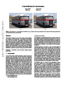
Finding the sampling frequency to simultaneously downconvert multiple bandpass signals using bandpass sampling is not straightforward. For N bandpass signals, a numerical solution ¡ ¢ for the sampling frequency is obtained by solving 3 + N2 constraint equations [3, Eq. (1) · · · (4)]. Often, these constraints can lead to considerable oversampling requirements i.e., the solution needs much higher sampling frequency than the sum of sampling rates required by all desired signals. Higher sampling rate not only increases the ADC complexity but also requires higher DSP speeds, thereby also increasing the power consumption. Moreover, the complexity of finding an appropriate sampling frequency is high and is clearly shown in [5] for a two channel system. It is easy to see that such methods will become increasingly more complex and solution for sampling frequency harder to find with increase in the number of channels. We propose an alternative front-end scheme that offers several advantages over bandpass sampling for directly downconverting multiple bandpass signals. We present our scheme in section II, suggest a realization of down-conversion function in section III, provide simulation results in section IV, make some general remarks about the scheme in section V and conclude in section VI. II. P ROPOSED S CHEME We will use a novel function, referred to as the downconversion function, to mechanise the front-end of the receiver in such a way that the signal received by the digital hardware for the proposed scheme is in no way different from the signal received by the digital hardware in a conventional single channel receiver. In the digital domain the usual lowpass or matched filtering is assumed. Let the N bandpass signals of interest be −1 th {mi (t) cos 2πfc,i t}|N baseband i=0 , where mi (t) is the i signal with bandwidth Wi and fc,i is its carrier frequency. We propose a receiver front-end for the simultaneous and direct down-conversion of these N signals. As shown in Fig. 1, the received signal is passed through a bandpass filter array to allow only the N signals of interest to pass through. Let Wmax be the bandwidth of the signal with the maximum bandwidth, amongst the N signals being considered. For the present we assume that each bandpass filter (BPF) in the array is ideal and its bandwidth B is equal to Wmax . The output of the filter array is given by
c 2006 IEEE 1536-1276/06$20.00 °
rBPF (t) =
N −1 X i=0
mi (t) cos 2πfc,i t
(1)
2
IEEE TRANSACTIONS ON WIRELESS COMMUNICATIONS, VOL. 5, NO. 2, FEBRUARY 2006
x 0 [n]
r(t)
BPF BPF 22
.. .
+
LNA
×
s(t)
AAF
s F (t)
ADC
d(t)
Downconversion Function
BPF N
Fig. 1.
r BPF (t)
x [n]
Demultiplexer
Analog
BPF 1
LPF
y 0 [n]
.. Digital . x i [n]
LPF
y i [n]
.. . LPF
y N − 1 [n]
x N − 1 [n]
Block diagram for the proposed receiver
This is passed through a low noise amplifier and then multiplied by a down-conversion function d(t). The downconversion function has to bring all the messages to baseband, so it can be of the form d(t) =
N −1 X
k=0
gi (t) cos 2πfc,i t
(2)
i=0
where gi (t) is a baseband signal. Multiplying rBPF (t) with d(t) gives s(t) = rBPF (t)d(t) =
N −1 1 X mk (t)gk (t) 2
+
k=0 N −1 N −1 X X
1 2
k=0 m=0
N −1 N −1 1 X X mk (t)gm (t) cos 2π(fc,k+fc,m )t 2 m=0 k=0
(3)
The signal s(t) is passed through an anti-aliasing filter which should be able to filter out the double summation terms. This is possible only when |fc,k −fc,m | for all k and m is greater than certain minimum value, which we call minimum frequency separation. We determine the minimum frequency separation required, in Appendix II. For the moment we assume that the |fc,k −fc,m | is large enough for the last two terms to be easily filtered. The filtered s(t) is given by, sF (t) =
N −1 1 X mk (t)gk (t) 2
The down-conversion function d(t) is to be designed such that these N digital signals are the sampled versions of the corresponding message signals mi (t). In the remaining parts of this section we consider the design of the down-conversion function d(t), the constraints on the anti-aliasing filter, minimum frequency separation required and finally consider ways for reducing the complexity of the bandpass filters. A. Design of Down-conversion Function
mk (t)gm (t) cos 2π(fc,k−fc,m )t
m6=k
+
digital filters is to remove the out of band noise from the digital signals, leaving the message unaffected. Thus, µ ¶ µ ¶ N −1 nN + i nN + i 1 X mk gk (6) yi [n] = 2 RS RS
(4)
k=0
This is sampled at a rate RS , which can be as low as N Wmax samples/sec. We can increase RS to simplify the design of bandpass filter, as shown in Section II-E. After sampling we get, ¶ µ n (5) x[n] = sF RS which is demultiplexed into N different digital channels, −1 {xi [n]}|N i=0 . This demultiplexing downsamples each channel by a factor of N with a suitable phase shift. The downsampled signals, having a sample rate of RNS , are passed through digital lowpass filters with bandwidth equal to the corresponding −1 message bandwidth, giving {yi [n]}|N i=0 . The purpose of these
The baseband signals gi (t)s are to be chosen such that yi [n] in (6) is the sampled version of the corresponding message signal mi (t), i.e., µ ¶ nN + i yi [n] = λ · mi (7) RS where λ is some constant. If this is possible then yi [n] is not different in any way to the digitized baseband signal in a conventional single channel receiver. For convenience we assume a symmetric form for the down-conversion function d(t) wherein all the gi (t) are just time shifted versions of each other, i.e., µ ¶ i gi (t) = g0 t − (8) RS Thus we only need to design g0 (t), and then we can use (2) and (8) to obtain d(t). General Down-conversion Function Consider a periodic function g0 (t) having H harmonics with its Fourier Transform of the form ¶ µ H X RS (9) G0 (f ) = ck δ f − k N k=−H
A sufficient condition that the down-conversion function d(t), obtained from this g0 (t) using (8) satisfies (7) is given by b H−m c N
X
cm+kN = K,
k=−b H+m N c
¹ º¾ ½ ¹ º N N ,..., (10) ∀m = − 2 2
MAHAJAN et al.: A NOVEL METHOD FOR DOWN-CONVERSION OF MULTIPLE BANDPASS SIGNALS
where K is some constant and ¹ º N H≥ 2
3
(11)
We prove this result in Appendix I. B. Minimum Frequency Separation Required The Fourier transform of d(t), D(f ) is spread out around each of the carrier frequencies. In general when we multiply d(t) with rBPF (t), the product s(t) may experience interference amongst the N message signals. However, if the signals have some separation in their carrier frequencies this situation can be avoided. It is shown in Appendix II that a minimum frequency separation given by ∆fmin = max {∆fi,j } = 2H i,j
RS B Wmax + + N 2 2
(12)
will prevent interference amongst the signals. Note that the carrier frequencies need not be equi-spaced. However the separation between any two of them should be greater than the minimum value obtained from (12). The Optimal Solution: We want to optimize the downconversion function such that the minimum frequency separation required is lowest possible. To minimize ∆fmin given by (12), we must minimize H. Now according to (11), the minimum value of H is b N2 c. Thus, ¹ º N H opt = (13) 2 Solving for G0 (f ) subject to the constraints (10) (assuming K = 1) and (A8) for H = b N2 c, we get1 Gopt 0 (f )
1 = N
bN 2 c
X
n=−b N 2 c
¶ ³n´ µ RS δ f −n rect N N
(a) Plot of g0 (t) cos 2πfc,0 t. The dashed envelope shows g0 (t).
(b) Plot of g1 (t) cos 2πfc,1 t. The dashed envelope shows g1 (t).
(c) Plot of g0 (t) cos 2πfc,0 t + g1 (t) cos 2πfc,1 t. Both the envelops g0 (t) and g1 (t) are shown.
(14)
Taking the inverse Fourier transform we obtain, g0opt (t)
k=b N X2 c ¡ ¢ ¡ ¢o 1n k = 1+2 rect N cos 2π kR t S N N
(15)
k=1
Using (8), we get giopt (t)
k=b N X2 c ¡ ¢ ¡ ¢o 1n rect Nk cos 2π = 1+2 k(RS t − i) (16) N N k=1
From (12), we obtain that the minimum frequency separation for the case of optimal d(t) is given by ¹ º N RS B Wmax opt ∆fmin = 2 + + (17) 2 N 2 2 C. Example of Optimal Down-conversion function Suppose there are N = 5 message signals to be downconverted. Parts g0 (t) and g1 (t) of the optimal downconversion function for this case, as given by (16), are shown in Fig. 2(a) and 2(b). It can be seen that here gi (t) peaks at only those sampling instants where the ith channel is to be sampled and is zero at sampling instants of other channels. 1 We
¡ ¢ follow the convention that rect ± 12 =
1 . 2
(d) Plot of d(t). All the envelopes g0 (t), g1 (t), g2 (t), g3 (t) and g4 (t) are shown. Fig. 2.
Down-conversion function.
Since the number of channels is five, gi (t) will have a peak at every fifth sampling instant and four zeros at the sampling instants in between. The overall down-conversion function is a sum of five similar gi (t)s upconverted to different carrier frequencies. The sum of g0 (t) and g1 (t) after upconversion to fc,0 and fc,1 is shown in Fig. 2(c). Fig. 2(d) shows the complete down-conversion function d(t) along with all the envelopes gi (t). It is important to note the difference between the N is even and N is odd cases. Although H remains the same for N = 2k and N = 2k+1 for integer k, there is a difference between the down conversion functions as shown here by example. Fig. 3 shows the Fourier Transforms D4 (f ) and D5 (f ) of the downconversion function for the cases N = 4 (even) and N = 5 (odd). From (13), we get Hopt = 2 for both cases. However, for
4
IEEE TRANSACTIONS ON WIRELESS COMMUNICATIONS, VOL. 5, NO. 2, FEBRUARY 2006
RS 4
1/4
D 4( f ) 1/8 f c,0
f c,1
f c,2
f c,3
fc,0
RS 5
Fig. 4.
f c,0
f c,1
f c,2
f c,3
passband
fc,i
fc,N− 1
B
bandwidth
f
(a) Fourier Transform of Down-Conversion function for N = 4
D 5( f ) 1/5
Wmax
f c,4
f
Bandpass filter.
f
(b) Fourier transform of down-conversion function for N = 5 Fig. 3. Fourier transforms of down-conversion function for N = 4 and N = 5.
even N, for all the gi (t)s the amplitude of the highest cosine is half the amplitude of other cosines, as can be seen from Fig. 3(a). This is because for even N , the highest frequency corresponds to the ‘edges’ of the rect function, so their value is half of the maximum. For odd N, all the cosines in gi (t) have the same amplitude as can be seen from Fig. 3(b).
and bandwidth of the bandpass filter should be chosen so as to avoid this aliasing. At the same time, the filter must allow the signal of interest to pass undistorted. Hence, the passband, centered around the carrier frequency, must have a width larger than the message bandwidth. Thus B > Wmax . Moreover, ± when Wmax < B < RS N , the signal ±is not aliased, as shown in Fig II-E. Furthermore, if B > RS N , this ± multiplication causes aliasing. However, for B < 2RS N − Wmax , this aliasing does not distort the message signals as shown in Fig. II-E. Hence for the message signals to remain undistorted Wmax ≤ B < 2
D. Anti-Aliasing Filter Bandwidth anti-aliasing filter must allow the baseband signal PThe N −1 m k (t)gk (t) to pass undistorted. Moreover, it should k=0 not allow any part of the signal that comes as a result of frequency difference terms in (3) to pass, as they can cause aliasing. Thus, the bandwidth of the anti-aliasing filter WF , should be between FRi,j and FLi,j , shown in Fig. 9 and given by (A16) and (A17). Hence, ½ ¾ RS Wi Wj RS B H + max + ≤ WF ≤ ∆fi,j − H − N 2 2 N 2 (18) RS Wmax RS B ⇒H + ≤ WF ≤ min{∆fi,j } − H − (19) N 2 N 2 The output of the anti-aliasing filter is fed into the ADC. We observe that the input to the ADC is a baseband signal as opposed to bandpass sampling where the input to the ADC is an RF signal. This considerably simplifies the design of the ADC, as further discussed in Section V . E. Bandpass Filter and Reducing its Complexity A bandpass filter is characterized by its center frequency, passband width and bandwidth (refer to Fig. 4). In this section, we explain the necessity of a bandpass filter array and determine the constraints on the passband width and bandwidth of the filters. A bandpass filter array is needed to avoid aliasing when rBPF (t) is multiplied with the down-conversion function. For simplicity we assume that all the filters have the same bandwidth B. The minimum frequency separation (Section II-B) ensures that there is no interference amongst the different components of rBPF (t), i.e. the component of rBPF (t) centered at fc,i will not interfere with the component centered at fc,j , ∀j 6= i, after multiplication with d(t). However, the component centered at fc,i can still be aliased when multiplied with the component gi (t) cos 2πfc,i t of d(t). The passband
RS − Wmax N
(20)
The filter response between fc,i ± W2max and fc,i ± B2 need not be flat. This means that we can increase the transition band of the filter, without introducing any additional noise in the message bandwidth. A larger transition band simplifies the design of the filter. This leads to a useful trade-off between ADC design and filter design. The design of the filter can be simplified by increasing the sampling rate which will lead to an increase in the complexity of the ADC. Let us consider an example to illustrate the flexibility provided by this trade-off. Assume that there are N = 2 signals, each of bandwidth Wi = 2MHz. Suppose we want to keep the ADC as simple as possible. This means that we need a sampling rate RS of N Wmax = 4 M samples/sec. At this sampling rate, the maximum bandwidth of the BPF that we can have, without causing aliasing, is Bmax = 2 RNS − Wmax = 2 MHz. Assuming the carrier frequency to be of the order of 1 GHz, we need to realize a BPF with Q ∼ 1G/2M = 500 which can be difficult to realize. Now assume that we can easily realize filters with Q ∼ 50. So we need to have a BPF with B = 20 MHz and RS = N2 (B + Wmax ) = 22 Msamples/sec, thereby increasing ADC complexity. Thus one can trade-off filter complexity with ADC complexity. Table I shows the flexibility available in the choice of the bandwidth of the bandpass filter at the cost of a higher sampling frequency and larger ∆fmin . In this table, the minimum frequency separation corresponds to its minimum possible values, employing the optimal downconversion function as derived in Section II-B. III. R EALIZATION OF D OWN -C ONVERSION F UNCTION In this section, we present a very simple method of realizing the down-conversion function, thus emphasizing the simplicity of this seemingly complex function. The realization of the down-conversion function can be divided into two parts, the
Down Conversion Function
Output of andpass Filter
MAHAJAN et al.: A NOVEL METHOD FOR DOWN-CONVERSION OF MULTIPLE BANDPASS SIGNALS
Width of BPF R BPF ( f )
RS N
After Multiplication
fc, i
f c, i +
f
RS N
fc,i
RS N
RS N
0
Message Signal
Fig. 6.
˜
˜ 1 fc,N−
Lowpass Block
f
d(t)
+
×
(RS , N)
S (f )
˜ ×
Cosine Sources
G i (f )
− Output of Bandpass Filter
fc,0 gi (t) Generator
f
Wmax B
Dowm Conversion Function
×
90º Phase Shift
Message Signal
fc, i −
RF Block
Hardware implementation for the down-conversion function.
TABLE I T RADEOFF BETWEEN FILTER BANDWIDTH (B) AND SAMPLING FREQUENCY (RS )
Width of Bandpass Filter
R BPF ( f )
f Gi ( f )
RS N
fc, i − After Multiplication
5
fc, i
f c, i +
No. of Signals N
Sampling Freq RS (M spl./sec)
Bandwidth B (MHz)
Min. freq. separation ∆fmin (MHz)
2 2 5 5
4 22 10 55
2 20 2 20
6 33 10 55
f
RS N
S(f)
f
W max B −
RS N
of weights given by (22) to get gi (t). Then the gi (t)s are up-converted and added to get the down-conversion function d(t). The block diagram of this scheme is shown in Fig. 6. Though this is a realization for the special case of the optimal solution (Section II-B), this idea can also be used to generate the general baseband gi (t).
RS N
0
Fig. 5. Fourier transform of signal after bandpass sampling and multiplication with the down-conversion function.
generation of the baseband signals gi (t)s and combining them to generate d(t). For the generation of gi (t) in the optimal solution case, consider (16)
gi (t) =
1 N
j k N k= 2
(
1+2
X
rect
¡ k ¢h N
cos
¡ 2π ¢ ¡ 2π ¢ N i cos N kRS t
k=1
¡ ¢ ¡ 2π ¢i i sin kR t + sin 2π S N N
=
1 N
j
(
N X2
k
k=
1+2
rect
¡k¢ N ×
k=1
¢ ¡ 2π ¢¢ ¡ ¡ Ai cos 2π N kRS t + Bi sin N kRS t where, Ai = cos
µ
¶ 2π i N
)
µ and
Bi = sin
¶ 2π i N
) (21)
(22)
From (21) we get that gi (t) is a weighted sum of low frequency sine and cosine functions. We generate the sines S and cosines of frequency kR and add them in the ratio N
IV. S IMULATION R ESULTS We simulated the proposed front end scheme by simultaneously down-converting N channels using the optimal (in terms of the lowest ∆fmin ) down-conversion function derived in Section II. The signals were initially modulated using uncoded BPSK, received over an AWGN channel, down-converted using the proposed scheme, sampled using an ideal ADC and demodulated using digital matched filtering. In one simulation we varied the number of channels N , each having a data rate Rb of 1 Mbp. We chose the bandpass filter bandwidth2 as 5 MHz and the digital processing rate of each demultiplexed channel RS /N as 10 samples/(bit duration) (=10 M samples/sec), regardless of the value of N . The bandwidth of the anti-aliasing filter WF was chosen to be (bN/2c · 10 + 4) MHz. It can be seen that this choice satisfies (19). Fig. 7 shows the performance curves of the proposed receiver, for two, three and five channels along with the performance curve of the conventional single channel receiver drawn for reference. It is clear from the figure that the performance is independent of the number of channels and is same as that for a conventional receiver. In another simulation we fixed the number of channels to two and simulated for three different bandwidths that satisfied (20). We again used messages with data rate Rb of 1 Mbps and digital processing 2 We chose B to be larger than the minimum required by a data rate of 1 Mbps to ease the design of the bandpass filter (refer Section II-E).
6
IEEE TRANSACTIONS ON WIRELESS COMMUNICATIONS, VOL. 5, NO. 2, FEBRUARY 2006
−1
10
BER
Conventional 2 Channels 3 Channels 5 Channels
−2
10
−3
10
1
1.5
2
2.5
3
3.5 SNR
4
4.5
5
5.5
6
5.5
6
Performance for different values of N .
Fig. 7. −1
10
Conventional B < R s /N B = R s /N
BER
B > R s /N
−2
10
−3
10
1
Fig. 8.
1.5
2
2.5
3
3.5 SNR
4
4.5
5
Performance for different bandwidths of the BPF for N = 2.
rate RS /N of 10 M samples/sec. Since N was taken to be two, this means that the sampling rate RS was 20 M samples/sec. WF , the bandwidth of the anti-aliasing filter was fixed at 14 MHz. The result is shown in Fig. 8 along with the curve for a conventional system. We observe that the performance does not get affected by the width of the bandpass filter, if it is within the bounds derived in (20). V. D ISCUSSION There are no issues of cross-talk from the theoretical perspective. We have assumed ideal filters and not taken into account the possible phase distortion caused by the anti-aliasing filter, which will lead to deviation from this zero cross-talk behavior. However, this distortion can be pre-compensated while generating the down-conversion function or computationally removed in the digital domain. Furthermore, for zero crosstalk, the carrier frequencies of the message signals must be separated by more than the minimum frequency separation given by (17). This however is not a major limitation as in most cases, ∆fmin can be designed to moderate values (see Table I). Moreover if the signals are located very close to
each other, they can be considered as a single message signal, down-converted together as a single band and separated in digital processing, as is done in wide-band receivers [6]. In some applications it may be desirable to choose the downconversion function so as to minimise the errors due to jitter which, in turn, will also lead to cross-talk. The errors because of jitter would depend on the slope of the baseband gi (t) at its zero crossings. But the slope alone cannot be the criterion for choosing gi (t) as its bandwidth will have implications on the minimum frequency separation required. In section III, a simple architecture for generating the down-conversion function was presented. Although we have not looked into all the details required for the hardware implementation of the proposed scheme, yet there are some inherent advantages over bandpass sampling technique vis-avis ADC and bandpass filter design. In bandpass sampling, ADC has RF input, while in the proposed scheme it has a baseband signal as input. Designing an ADC for an RF input is harder as it is difficult to implement sample and hold circuit for high analog frequencies. Furthermore, a bandpass sampling receiver is very prone to thermal noise. A typical bandpass sampling receiver architecture consists of a stage, either a BPF array or a subsequent buffer stage, which drives the ADC analog input. The output impedance of this stage, typically 50 Ohm, feeds white thermal noise into the ADC. An ADC with RF input has a very small input capacitance and hence a large noise power is sampled [2]. Since the output bandwidth of the ADC is low, as the signal is being undersampled, this large noise power is distributed over a much smaller bandwidth, thereby reducing the effective SNR. Even in our scheme the digital demultiplexing, which is equivalent to undersampling, would multiply the power of the thermal noise from the stage driving the ADC. However the multiplication factor will be equal to the number of channels being down-converted in the system (∼2-10), which is small and the total noise would still be dominated by the channel noise. On the contrary in bandpass sampling systems, downsampling factors can be expected to be huge (∼50-1000), thereby leading to significant increase in thermal noise. Moreover, bandpass sampling requires bandpass filters having a high Q-factor. In our scheme if we use such high Q-factor filters, we can operate the ADC at a rate close to the sum of Nyquist rates of all messages. More importantly, in our scheme the design of bandpass filters can be simplified by oversampling, as discussed in Section IIE. In practical digital receivers oversampling is inherently needed for phase and timing recovery, thus bandpass filter design can be simplified without drastically increasing the ADC complexity. Furthermore, bandpass sampling needs to separate different messages computationally during the digital processing. In the proposed scheme, different messages are separated by the simple operation of demultiplexing. Thus the amount of DSP computation required is same as that in a conventional receiver, and considerably less than what is required in bandpass sampling. VI. C ONCLUSION In this paper we have proposed an alternative to bandpass sampling using a novel down-conversion function, to directly
MAHAJAN et al.: A NOVEL METHOD FOR DOWN-CONVERSION OF MULTIPLE BANDPASS SIGNALS
down-convert N message signals which have certain minimum frequency separation. The design of the system has been discussed and all the proposed blocks have been explained. The proposed system provides several advantages in terms of sampling rate, Band Pass Filter and ADC requirements.
7
as gi (t) is the sampling function for mi (t) with a sampling period of RNS ). This implies that the Fourier transform of g0 (t) is of the form H X
G0 (f ) =
k=−H
R EFERENCES [1] R. Berezdivin, R. Breing, and R. Topp, “Next-generation wireless communication concepts and technologies,” IEEE Commun. Mag., vol. 40, no. 3, pp. 108–116, 2002. [2] R. G. Vaughan, N. L. Scott, and D. R. White, “The theory of bandpass sampling,” IEEE Trans. Signal Processing, vol. 39, pp. 1973–1984, Sept. 1991. [3] D. M. Akos and M. Stockmaster, “Direct bandpass sampling of multiple distinct RF signals,” IEEE Trans. Commun., vol. 47, pp. 983–988, July 1999. [4] N. Wong and T. S. Ng, “An efficient algorithm for down-converting multiple bandpass signals using bandpass sampling,” in Proc. IEEE International Conference on Communications, vol. 3, 2001, pp. 910–914. [5] C. H. Tseng and S. C. Chou, “Direct downconversion of multiple RF signals using bandpass sampling,” in Proc. IEEE International Conference on Communications, vol. 3, 2003, pp. 2003–2007. [6] Rhode, Ulrich, and et al., Communication Receivers, 3rd ed. New York: McGraw-Hill, 2002.
A PPENDIX I G ENERAL S OLUTION OF THE D OWN - CONVERSION F UNCTION We want the down-conversion function (2) to be such that we get the desired output (7), µ ¶ nN + i yd,i [n] = λ · mi (A1) RS
¶ µ RS ck δ f − k N
(A7)
where H is the number of harmonics. Since g(t) is real, the Fourier coefficients should also have conjugate symmetry. Thus, cp = c∗−p
∀p ∈ {−H, . . . , H}
(A8)
Any function gi (t) of the form (A7) that satisfies (A2) and (A3) can be used in (2). Taking Fourier Transform of (A4) we get, ∞ ´ ³ω X RS − kRS ∀ ω ∈ (−π, π] G0 2π k=−∞ (A9) where G(ejω ) is the DTFT of g[n] and G0 (f ) is the Fourier Transform of g0 (t). Substituting (A7) in (A9), we get
=⇒ G(ejω ) = RS
∞ X
jω
G(e ) = RS RS
H X
µ cm δ
k=−∞ m=−H
µ
bN 2 c
X
bm δ
RS ω RS − kRS − m 2π N
ω RS RS − m 2π N
¶ when H ≥
¥N ¦ 2
m=−b N where λ is some constant. In this appendix, we will derive = 2 c , µ ¶ H X a class of solutions for g(t) under the constraint that g(t) is ¦ ¥ ω R S cm δ RS − kRS − m when H < N2 RS symmetric (8) and the output of the receiver is given by (7). 2π N n=−H To get the desired output we can choose gi (t) satisfying, (A10) ( µ ¶ λ if n ≡ i (mod N ) n gi = , for 0 ≤ i ≤ (N −1) for all ω ∈ (−π, π] where RS 0 otherwise (A2) We assume that all the gi (t) are just time shifted versions of b H−m c N X © ¥ ¦ ¥ ¦ª each other, that is bm = cm+kN , ∀ m = − N2 , . . . , N2 (A11) ¶ µ i k=−b H+m c N gi (t) = g0 t − (A3) RS Thus we only need to solve for g (t) and using (A3), we can Combining (A10) and (A6), gives 0
find all gi (t)s. Let
µ g[n] , g0
n RS
¶ (A4)
For H ≥ b N2 c, For H < b N2 c,
(A2) implies that
( λ g[n] = 0
if n ≡ 0 (mod N ) otherwise
(A5)
Taking DTFT gives, G(ejω ) =
2πλ N
Let K =
2πλ N RS .
© ¥ ¦ ¥ ¦ª 2πλ , ∀ m = − N2 , . . . , N2 N RS inconsistent equations (A12) bm =
Then, (A11) and (A12) imply
c b H−m N
µ
bN 2 c
X
m=−b N 2 c
δ
RS ω RS − m 2π N
X
¶ (A6)
Now, we can assume that gi (t)s are periodic functions with a time period of RNS . (This is a reasonable assumption to make,
cm+kN = K
© ¥ ¦ ¥ ¦ª ∀ m = − N2 , . . . , N2
k=b H+m N c
(A13) ¹ H≥
N 2
º (A14)
8
IEEE TRANSACTIONS ON WIRELESS COMMUNICATIONS, VOL. 5, NO. 2, FEBRUARY 2006
The extreme left alias (message signal along with all the undesirable signal allowed by the BPF) of Mi (f ) ∗ Gj (f ± ∆fi,j ) + Mj (f ) ∗ Gi (f ± ∆fi,j ) will be at
B S(f )
Mj
Mi
fc,i
fc, j
f
Wi
D(f )
··· ··· fc,i
··· ··· fc, j − H RNS
fc,i + H RNS
fc, j
f
Fx Baseband Signal
··· ···
··· ···
0
fc,i − fc, j FRi, j
Fig. 9.
FLi,j = ∆fi,j − H
B RS − N 2
(A17)
As seen from Fig. 9 to avoid aliasing Fx = FLi,j − FRi,j ≥ 0. Thus, ½ ¾ RS B Wi Wj ∆fi,j = |fi −fj | ≥ 2H + +max , for all i, j N 2 2 2 Thus, ∆fmin = max {∆fi,j }
f
FLi, j
i,j
= 2H
Fourier transform of s(t) and d(t).
A PPENDIX II M INIMUM F REQUENCY S EPARATION Let S(f ) and Gi (f ) be the Fourier Transform of s(t) and gi (t) respectively. From (3) we get that,
RS B Wmax + + N 2 2
(A18)
Aditya Mahajan received his B.Tech. degree in Electrical Engineering from Indian Institute of Technology Kanpur, India in 2003. He is currently working towards a Ph.D. in Electrical Engineering and Computer Science from University of Michigan, Ann Arbor, Michigan. His research interests include real-time communication systems and stochastic decision theory.
N −1 1 X Mk (f ) ∗ Gk (f ) S(f ) = 2 k=0 N −1 N −1 X X
1 + 4
Manu Agarwal received his B.Tech. degree in Electrical engineering from the Indian Institute of Technology, Kanpur, India in 2003 and his M.S. Degree in Electrical Engineering from Stanford University, Stanford, California in 2005. He is currently working toward a Ph.D. degree in Electrical engineering at Stanford University. During his undergraduate career he interned at the Technical University of Ilmenau in Germany and at the EPFL, Switzerland. During his graduate career, he has interned at Agilent Labs in Palo Alto, CA, on characterizing dipole surface drive MEMS actuators. His current research interests include design of high frequency MEMS resonators for frequency references and analog circuit design.
Mk (f ) ∗ Gl (f − ∆fk,m )
k=0 m=0 m6=k
+
1 4
N −1 N −1 X X
1 4
N −1 N −1 X X
1 4
N −1 N −1 X X
Mk (f ) ∗ Gl (f + ∆fk,m )
k=0 m=0 m6=k
+
Mk (f ) ∗ Gl (f − fc,k−fc,m )
k=0 m=0 m6=k
+
Mk (f ) ∗ Gl (f + fc,k+fc,m )
(A15)
k=0 m=0 m6=k
The signal at ∆fi,j = |fc,i − fc,j | should not overlap with PN −1 the message signals at the baseband k=0 mk (t)gk (t). Thus ∆fi,j should be large enough so that mi (t)gj (t)cos2π∆fi,j t PN −1 does not overlap with k=0 mk (t)gk (t). The Fourier Transform of S(f ) is shown in Fig. 9. We assume that B ≥ Wmax and G0 (f ) is of the form (A7). The last (extreme right) alias (message only) of Mi (f ) ∗ Gi (f ) + Mj (f ) ∗ Gj (f ) will be at ½ ¾ Wi Wj RS + max , (A16) FRi,j = H N 2 2
Ajit K. Chaturvedi (S’91-M’96-SM’03) received his B.Tech., M.Tech., and Ph.D. degrees in Electrical Engineering from Indian Institute of Technology Kanpur in 1986, 1988, and 1995, respectively. He was a faculty member in the Department of Electronics Engineering at Institute of Technology, Banaras Hindu University, Varanasi, India from 1994 to 1996. Subsequently, he joined the faculty of the Department of Electronics and Computer Engineering at University of Roorkee, Roorkee (now Indian Institute of Technology Roorkee). Since 1999 he has been teaching in the Department of Electrical Engineering at Indian Institute of Technology Kanpur. His research interests are in the area of communication theory, spread spectrum systems and wireless communications. Dr. Chaturvedi has been actively involved in the Uttar Pradesh section of IEEE. He has served the section in several capacities and is presently its Chairman.