528
JOURNAL OF MICROELECTROMECHANICAL SYSTEMS, VOL. 9, NO. 4, DECEMBER 2000
A Novel Parametric-Effect MEMS Amplifier Jean-Pierre Raskin, Member, IEEE, Andrew R. Brown, Member, IEEE, Butrus T. Khuri-Yakub, Fellow, IEEE, and Gabriel M. Rebeiz, Fellow, IEEE
Abstract—This paper presents the theory and measurements of a mechanical parametric-effect amplifier with a 200-kHz input signal and a 1.84-MHz output signal. The device used is a MEMS time-varying capacitor which is composed of an array of low-stress metallized silicon-nitride diaphragms, and is pumped by a largesignal voltage at 1.64 MHz. This induces a large change in the capacitance, and results in parametric amplification of an input signal at 200 kHz. The parametric amplifier capacitance is 500 pF, resulting in an output impedance of 140 . A higher impedance can also be achieved with a lower capacitance. To our knowledge, this device is the first-ever MEMS mechanical up-converter parametric-effect amplifier developed with an up-conversion ratio of 9 : 1. The measurements agree very well with theory, including the effect the series resistance and the of the MEMS time-varying capacitor. The application areas are in amplifiers which operate at very high temperatures (200 C–600 C), under high particle bombardment (nuclear applications), in non-semiconductor-based amplification, and in low-noise systems, since parametric amplifiers do not suffer from thermal, shot, or 1/f noise problems. [571]
I. INTRODUCTION
P
ARAMETRIC-EFFECT devices, based on nonlinear reactances such as capacitors and inductors, have been extensively used in the 1960s for amplification, frequency upand down-conversion, and oscillators at microwave frequencies [1], [3]. Parametric devices transfer the power from the pump frequency ( ) to the signal frequency ( ), as opposed to standard amplifiers which transfer power from the dc source to the signal frequency. Parametric amplifiers were commonly built using varactor diodes for microwave applications. Since parametric amplifiers are not based on semiconductor junction effects and resistors, they do not suffer from the Johnson, Shot, and 1/f noise, resulting in low-noise amplifiers [3], [6]. With the introduction of MESFETs, parametric amplifiers were abandoned and, to our knowledge, they are not used anymore in microwave applications. However, in recent years, the parametric amplification has seen a resurgence mostly in optical systems [7], [8]. This paper presents a micromechanical (MEMS) up-converter parametric-effect amplifier. The MEMS time-varying capacitor is composed of a thin low-stress metallized silicon–nitride diaphragm and is pumped by a large-signal voltage at a pump frequency . This results in large changes in the Manuscript received May 3, 2000; revised August 7, 2000. This work was supported by the DARPA Sonoelectronics Program under Contract DAAG55-98-10432 and by the Army Research Office under Contract DAAG55-98-10432. Subject Editor, N. deRooij. J.-P. Raskin is with the Microwave Laboratory, Université catholique de Louvain, Louvain-la-Neuve, Belgium (e-mail:
[email protected]). A. R. Brown and G. M. Rebeiz are with Radiation Laboratory, The University of Michigan, Ann Arbor, MI 48109-2122 USA. B. T. Khuri-Yakub is with Edward L. Gizton Laboratory, Stanford University, Stanford, CA 94305 USA. Publisher Item Identifier S 1057-7157(00)10175-1.
capacitance and parametric amplification of an input signal at . The design and analysis of this amplifier is presented in this paper, together with measurements of the transducer gain at 1.84 MHz. The theory of parametric amplification is first presented and the capacitance values, impedances, and amplifier gain are calculated for various frequencies. It is seen that the capacitance of the MEMS varactor determines the input and output impedance of the parametric amplifier, and to obtain high amplification, the MEMS capacitor must be pumped such that the capacitance component at the pump frequency is at least 30% of the dc capacitance. A detailed extraction technique based on – measurement of the MEMS capacitor under small- and large-signal conditions is then presented, and the capacitance, inductance, series resistance, and, most important, the capacitance variation are determined. These values are used in the construction and measurement of a 200-kHz input/1.84-MHz output parametric up-converter amplifier. The frequency of operation is controlled by the pump frequency (1.6 MHz, in this case), which can be increased up to 10–20 MHz by reducing the size of the MEMS diaphragm. The MEMS varactor is built using silicon micromachining techniques, but can also be integrated on ceramic, quartz, etc., substrates, resulting in a 10 kHz–10 MHz amplifier on nonsemiconductor based substrates. This may be excellent for building amplifiers for sensors (thermal, pressure, gravitational, chemical, nuclear, piezoelectric, etc.) without any CMOS electronics. Important advantages over CMOS based electronic amplifiers are the possibilities to operate at very high temperatures (control of the reaction rate in combustion chambers) and under high particle bombardment (nuclear applications) where CMOS electronics die after some time. Moreover, because parametric amplifiers do not suffer from thermal, shot, or 1/f noise problems, MEMS parametric amplifiers could be preferred to CMOS for building ultra-low-noise circuits. II. REVIEW OF PARAMETRIC AMPLIFICATION A. Manley–Rowe Equations Manley and Rowe have derived a very general pair of equations relating power flowing into and out of a one-port passive and lossless device with an arbitrary nonlinear characteristic [9]. These relations are a powerful tool in predicting whether or not power gain is possible in a given situation, and in predicting the maximum gain that can be achieved. The device is simuland a pump tanously fed by a signal source at frequency at the combination source at frequency . Active power is positive if it is fed to the nonlinear reactance, frequency and negative if it is delivered by the nonlinear reactance. Intuis applied to itively, when one external source of frequency
1057–7157/00$10.00 © 2000 IEEE
RASKIN et al.: A NOVEL PARAMETRIC-EFFECT MEMS AMPLIFIER
529
(a)
(b)
(c) Fig. 1. Amplitude spectra for parametric amplifier three-frequency operation. (a) Noninverting up-converter. (b) Inverting up-converter. (c) Inverting negative resistance amplifier.
the nonlinear capacitor, harmonic frequencies will be generated because of the nonlinear operation. Furthermore, in the presand , numerous new ence of two applied frequencies of are produced, where and are any frequencies of integers from zero to infinity. The manner of nonlinear interaction is similar to that which occurs in a nonlinear conductance device. The only new feature involved here is that no loss—or negligible loss—is considered with nonlinear susceptances, i.e., if power enters the nonlinear capacitor at the pump frequency, the same amount of power must leave the capacitor at the other frequencies through the nonlinear interaction. General analytical energy relations of nonlinear susceptances were comprehensively treated by Manley and Rowe in [9]. Their final results can be summed up in the following two equations: (1) (2) These relations are remarkable in that they are independent of the shape of the nonlinear characteristic and the power levels involved. The usefulness of these relations can be illustrated by several cases in which power flow at only three frequencies is allowed. By allowing only a single combination frequency besides the signal frequency and the pump frequency (all other combination frequencies are filtered), the general result (1) and (2) can be simplified. Two choices for are the following. upper sideband frequency, and 1) since and vary in the same direction, this is called the frequency-noninverting case, and results in (Fig. 1) (3) 2)
lower sideband frequency, and since and vary in opposite directions, this choice is called the frequency-inverting case (Fig. 1) (4)
Notice that the power gain is equal to the ratio of the output to input frequencies, and this can be as much as 10 : 1 or even
Fig. 2. Equivalent model and amplitude spectra for a generic parametric up-converter. The time-varying capacitance is pumped at ! , the input signal frequency is ! , and the up-converted frequency is ! ! ! . Since we consider ideal input and output filters, all other sidebands are terminated with an open-circuit.
=
+
50 : 1 depending on the choice of and . The output power is negative due to the definition of powers in the Manley/Rowe equations. B. Gain, Bandwidth, and Stability of Parametric Amplifier/Up-Converter The parametric amplifier is based on a time-varying capaci, which is pumped at and is defined by [11] tance
(5) is the dc capacitance of the MEMS capacitor and where are the Fourier-series coefficients which characterize the nonlinear behavior of the capacitance function. The time-varying capacitor is terminated in an ideal filter, such that signal volt, and ages at only the three frequencies , are allowed to exist. The noninverting case is of particular importance, since it can be proven [10] that the device is stable and yields maximum gain with a matched source and load impedance. Under matched conditions, the power gain is equal to the ratio of output to input frequencies as determined by the equations above. The transducer gain corresponding to the equivalent circuit presented in Fig. 2 is defined as the ratio of the output power in
530
JOURNAL OF MICROELECTROMECHANICAL SYSTEMS, VOL. 9, NO. 4, DECEMBER 2000
TABLE I SIMULATIONS FOR THE PARAMETRIC AMPLIFIER WITH DIFFERENT FREQUENCIES AND CAPACITOR VALUES
a load, ( (
), to the available input power from the source, ), and is calculated by [11] as
Manley and Rowe relationships (3) for the noninverting case. The input and output impedances become (13)
(6) being the two-port -parameters of the time-varying with , is the total external circuit impedance at capacitor ( ), and is the total external ( ). circuit impedance at and Neglecting the losses of the matching inductances ( ), the maximum transducer gain and bandwidth are obtained under the matched conditions defined as follows:
Note that the parametric amplifier does not result in an impedance transformation between the input and output ports, , even if the input and output frequencies and is dependent on are separated by a ratio of 10 : 1. Also, , and a low-impedance parametric amplifiers require a large-value MEMS capacitor. Under the matching conditions defined above, the maximum 3-dB gain bandwidth of the up-converter is independent of the capacitance and is given by (14)
(7)
(9)
The parametric amplifier can be designed to fit any transducer impedance by choosing the dc capacitance ( ) and the capac). Table I shows the calitance modulation ratio ( culated parameters for parametric amplifiers with varying , and . It is seen that a large gain and bandwidth can be obtained using parametric amplifiers at 100–1000 kHz, with an impedance anywhere from 50 k to 50 .
(10) (11)
III. MEMS VARACTOR FABRICATION PROCESS
(8)
with
and is given by (12) , and is the effective quality where ). factor of the time-varying capacitor ( , For the case of a lossless time-varying capacitor ( ), the transducer gain tends to the ratio , i.e., which is in accordance with the power gain defined from the
The central component of the MEMS parametric up-converter is a time-varying capacitor which consists of a thin diaphragm of metallized silicon nitride (top electrode) suspended above a heavily doped silicon bulk (bottom electrode). In order to decrease the magnitude of the pump signal voltage, the structure is made resonant at the pump frequency, the gap between the thin metallized silicon nitride diaphragm and the heavily doped silicon bulk is minimized (0.75 m), and the backside air loading (air between electrodes) is evacuated for reducing damping effects.
RASKIN et al.: A NOVEL PARAMETRIC-EFFECT MEMS AMPLIFIER
531
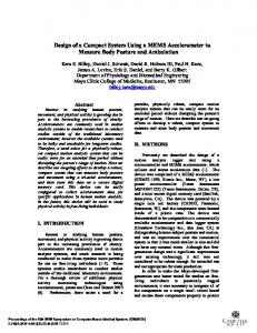
Fig. 3. Fabrication steps of the MEMS capacitor.
The main fabrication steps are shown in Fig. 3. An n-type (100) silicon wafer is heavily doped to achieve good conductivity at the wafer surface (defining the bottom electrode) and a 0.75- m oxide layer is grown with a wet oxidation process. This thin oxide layer is used as a sacrificial layer in the process. The oxide layer is patterned in order to define the diameter of the resonant silicon nitride membrane and etched using buffered hydrofluoric acid (BHF). A 6000-Å layer of LPCVD nitride is then deposited. The residual stress of the nitride can be varied by changing the proportion of silane to ammonia during the deposition process [2]. The residual stress obtained is around 170 MPa. A pattern of holes is then transferred to the wafer with an electron beam lithography process. The nitride is plasma etched and the sacrificial oxide is removed with BHF to release the silicon nitride diaphragm. A low-temperature oxide (LTO) layer is deposited and patterned on the released membrane, vacuum sealing the holes. Finally, aluminum is sputtered and patterned to act as the top electrode. The same aluminum deposition also defines bonding contacts to the bottom electrode through a lithographically defined trench in the silicon nitride layer. The fabricated capacitor is composed of 4500 orthogonally shaped silicon nitride membranes with 0.6- m thickness ( ), a residual stress ( ) of 170 MPa, 0.75- m gap ( ), and 50- m radius ( ). The total device area is around 1 cm . The cross section and top view of the built MEMS capacitor are presented in Fig. 4.
(a)
(b) Fig. 4. (a) SEM cross section. (b) Top view photograph of the built MEMS capacitor.
where mass of the movable structure in kilograms; damping coefficient in N s/m; spring constant in N/m; electrostatic applied external force in N. For a circular diaphragm, the coefficients are (16) (17)
IV. CHARACTERIZATION OF THE MEMS CAPACITOR The MEMS capacitor is modeled as a suspended resonator, and the system is described by the second-order differential equation (15)
is the density of the diaphragm material, the radius, the thickness of the diaphragm, is Young’s Modulus in pascals of the beam material, is the residual stress in the beam, and is Poisson’s ratio. The damping coefficient ( ) expresses the energy dissipation in the system by airflow force, squeeze force, internal friction,
and
532
Fig. 5.
JOURNAL OF MICROELECTROMECHANICAL SYSTEMS, VOL. 9, NO. 4, DECEMBER 2000
Simplified mechanical model of the MEMS time-varying capacitor.
and support loss, and is related to the mechanical quality factor ( ) of the mechanical structure as (18) Fig. 6.
Capacitance variation versus dc voltage.
A. Static Analysis The external electrostatic force ( ) is induced by the source voltage , and is applied between the two electrodes of the MEMS capacitor (19) Fig. 7. Small-signal electrical model of the MEMS capacitor.
where displacement of the membrane from the zero-voltage position; area of the membrane; gap between the two electrodes.
on the dc bias ( ), and this induces a small ac displacement . The dynamics of the resonator are approximately determined by the second-order ordinary differential equation (23)
In the electrostatic case, (15) is simplified as where
is the small-signal ac electrostatic force expressed by
(20) (24)
and (21) Fig. 6 shows the measured capacitance variation of the MEMS capacitor (described in Section III) versus dc bias , the increase in the electrostatic force conditions. At is much greater than the increase in the restoring force. Subinto (21), the “pull-down” or “collapse” stituting voltage is (22) The calculated collapse potential for the measured structure is 85 V. It is important to work under this limit to avoid the collapse of the capacitive membrane. B. Small-Signal Analysis In the linear case, we assume that the displacements ( ) are small compared to the physical gap dimension of the structure. , superimposed The capacitor is driven by a small ac voltage
and
. This results in (25)
is the phasor representation of the displacement, and is the resonant frequency. By analogy, the spring-mass-damping system in Fig. 5 can be represented by the equivalent small-signal electrical circuit represents the conductor losses in in Fig. 7. In this model, the capacitor plate and interconnect resistance. The capacitor current is
where
(26) and in phasor form (27)
RASKIN et al.: A NOVEL PARAMETRIC-EFFECT MEMS AMPLIFIER
533
Fig. 8. Setup measurement for the extraction of the MEMS capacitor small-signal electrical model.
is the ac small-signal applied across the capacitance , with From (25), the current is and
.
Fig. 9. Real part of 1=Y
versus frequency.
(28)
By comparing (25) and (28), the equivalent electrical elecan be related to the mechanical quantiments , , and ties as (29) (30) (31) The quality factor is given by (32) The device is first measured using an -parameter set-up and a low-frequency network analyzer (Fig. 8). The 50- -based two-port measurements are used to obtain the -parameters of the capacitor [5], and the equivalent model is extracted as described below. Far above the mechanical resonant frequency, the suspended . membrane does not vibrate with the ac small-signal voltage The equivalent admittance ( ) of the LCR series circuit therefore tends to zero (Fig. 7). Under high-frequency conditions, the can be simplified as inverse of the admittance (33) The quality factor of the MEMS capacitor is obtained by the 3-dB peak width method and the phase condition (34)
Fig. 10.
Equivalent capacitance (Y
=! ) around the resonant frequency.
The resonant frequency of the plate capacitor is extracted . is obtained directly from the following at subtraction:
(35) and capacitance can be exThe equivalent inductance and , respectively. At very low tracted by is frequency (a few kilohertz), the equivalent capacitance . obtained as and Figs. 9 and 10 represent the measured for the fabricated MEMS capacitor described in , , Section III. The extracted values obtained for , , are, respectively, 55 , 500 pF, 32.5 pF, 0.29 mH, and and 166 . The resonant frequency of the MEMS plate capacitor is 1.64 MHz and has a quality factor of 18.
534
JOURNAL OF MICROELECTROMECHANICAL SYSTEMS, VOL. 9, NO. 4, DECEMBER 2000
Fig. 12.
Scheme for extraction of C (t) expression.
, and the time-varying capacitance can be obtained numerically from
Fig. 11. Measured voltage time-varying capacitor C (t).
v(t)
(41)
and current i(t) flowing through the
Since
is a periodic function, it can be decomposed as
C. Large-Signal Analysis If a large pump signal voltage is applied, the displacements of the suspended diaphragm become nonnegligible compared to is generated the gap ( ), and a time-varying capacitance
(42) or
(36) when . The extraction of the Fourier with Series coefficients is an essential step for designing a parametric amplifier/up-converter. Two cases are considered: Case 1, with , and Case 2, with being substantial compared to . is small such that , the coefCase 1: If ficients can be extracted directly from the current spectrum magnitude (measured with a spectrum analyzer). The current through the time-varying MEMS capacitor with a voltage signal can be expressed as
Then, from the calculated numerical function and are extracted as coefficients
(44) (45) with (46)
(37) and the following expressions for the three first harmonics are obtained: (38) (39) (40) is not negligible, the current phase also needs Case 2: If and coefficients. The to be measured to determine the phase information can be obtained by the measurement of the and the current (Fig. 11). The current is voltage easily obtained by measuring the voltage across an external reconnected in series with the time-varying capacitor sistor (Fig. 12). (extracted from Knowing the value of the parasitic resistor is given by the small-signal analysis), the voltage across
(43) (36), the
From (44) and (45), the coefficients given by
and
in (42) are
(47) (48) Fig. 13 shows the measured harmonics level at the 50- input of the spectrum analyzer for the MEMS time-varying capacitance pumped with an ac large signal with 1.64 MHz. Due to the high value of (55 ) as 400 ) compared to the equivalent impedance ( of the MEMS capacitor, the second extraction method is used. is presented in Fig. 14, and the coefficients The calculated and are found to be 0.22, 0.05, 0.01, 7 , 3 and 0.85 . with
RASKIN et al.: A NOVEL PARAMETRIC-EFFECT MEMS AMPLIFIER
Fig. 13. Spectrum of the current flowing through the MEMS time-varying 60 V and v 15 V. capacitor for V
=
=
Fig. 14. Time-varying capacitance versus time for V
= 60 V and v = 15 V.
V. MEMS PARAMETRIC UP-CONVERTER AMPLIFIER MEASUREMENTS Fig. 2 shows the experimental setup for the parametric amplifier. The input filter is a Chebyshev bandpass filter composed of three LC sections and is designed to pass 200 kHz. It presents a bandwidth of 40 kHz and an insertion loss of 0.9 dB. The MEMS capacitor is pumped with a large ac signal at 1.64 MHz. In order to avoid power loss from the input signal at 200 kHz, and from the output signal at 1.84 MHz, into the pump signal generator, a Chebyshev bandpass filter composed of three LC sections is connected in series with the pump signal generator. This filter presents a bandwidth of 100 kHz and an insertion loss of 3.6 dB (not important for the gain measurements). The output filter is also a Chebyshev bandpass filter composed of three LC sections centered at 1.84 MHz with a bandwidth of 100 kHz. It attenuates greatly the image frequency at 1.44 MHz ( 60 dB). The input and output filters are also designed to do 140 an impedance transformation: from the generator (
535
Fig. 15. value.
Parametric up-converter transducer gain versus the load resistance
Fig. 16.
Parametric up-converter transducer gain versus .
) to the equivalent input impedance of the time-varying ca( equal to pacitor 85 at the resonant frequency) for the input filter and from ( equal to the equivalent output impedance of 85 at the resonant frequency) to 140 ) for the output bandpass filter. the load ( The measured and simulated transducer gain of the parametric up-converter versus the load resistance is shown in bandpass filters losses, Fig. 15. After de-embedding the we observe a good agreement between measurements and simulations. The gain was measured with an input signal from 0.1 to 0.5 V and was found to be the same. The measured optimum load of 135 is in accordance with the value of 140 calculated using (7). The bandwidth of operation was limited by the input filter to 40 kHz. Fig. 16 represents the measured transducer gain versus the which depends on the pump signal power. For coefficient these measurements, the matching networks and filters has been . As predicted by the simulations, the optimized for
536
JOURNAL OF MICROELECTROMECHANICAL SYSTEMS, VOL. 9, NO. 4, DECEMBER 2000
transducer gain of the MEMS parametric up-converter increases in order to with . It is seen that one needs at least a obtain any substantial gain from the circuit. of 15 V was used to achieve a A pump-signal magnitude coefficient equal to 0.22. This corresponds to a power of 560 mW delivered by the pump generator at 1.64 MHz. This high value of power is linked to the low mechanical quality factor of the measured structure ( ). In our case, the air loading (air in the front volume of the diaphragm) is the main factor which contributes to the global damping term of the mechanical structure. Wang et al. [4] have shown that it is possible to achieve quality factors of 10 000 under vacuum condition at 1–2 MHz. For this high value of , a coefficient of 0.22 can of less than 1 V, resulting be reached with a pump signal in a supply power at the pump frequency of less than 2 mW. Therefore, the optimization of the MEMS time-varying capacitor package is an important issue for reducing the power consumed by the novel MEMS parametric up-converter. VI. CONCLUSION This paper presented the theory of operation of MEMS-based parametric amplifiers. The parametric amplifier is critically dependent on the capacitance variation, and an accurate technique is presented to determine the fourier coefficients of the MEMS capacitor under large signal conditions. A 200-kHz input/1.84-MHz output MEMS parametric amplifier with a measured gain of 6 dB was presented. In the future, it is possible to build higher frequency amplifiers (up to 1–5 MHz) using smaller area membranes. The advantage of this technique is that one can build amplifiers for sensors (thermal, pressure, acoustic, gravitational, chemical, etc.) without any CMOS electronics. Some applications include very high temperatures amplifiers (200 C–600 C), high particle bombardment (nuclear applications) amplifiers, and very low 1/f noise amplifiers.
[8] G. M. Gale, F. Hache, and M. Cavallari, “Broad-bandwidth parametric amplification in the visible: Femtosecond experiments and simulations,” IEEE J. Select. Topics Quantum Electron., vol. 4, pp. 224–229, Feb. 1998. [9] J. M. Manley and H. E. Rowe, “Some general properties of nonlinear elements—Part 1: General energy relations,” Proc. IRE, pp. 904–914, July 1956. [10] H. E. Rowe, “Some general properties of nonlinear elements—Part 2: Small signal theory,” Proc. IRE, pp. 850–860, May 1958. [11] L. A. Blackwell and K. L. Kotzebue, Semiconductor-Diode Parametric Amplifiers. Englewood Cliffs, NJ: Prentice-Hall, 1961.
Jean-Pierre Raskin (M’97) was born in Aye, Belgium, in 1971. He received the Industrial Engineer degree from the Instiut Supérieur Industriel d’Arlon, Belgium, in 1993, and the B.S. and Ph.D. degrees in applied sciences from the Université catholique de Louvain, Louvain-la-Neuve, Belgium, in 1994 and 1997, respectively. From 1994 to 1997, he was a Research Engineer at the Microwave Laboratory, Université catholique de Louvain, where he worked on the modeling, characterization, and realization of MMICs in silicon-on-insulator technology for low-power low-voltage applications. In 1998, he joined the EECS Department of The University of Michigan, Ann Arbor. He has been involved in the development and characterization of micromachining fabrication techniques for microwave and millimeter-wave circuits and microelectromechanical transducers/amplifiers working in hard environments. Since January 2000, he has been an Associate Professor at the Microwave Laboratory of the Université catholique de Louvain. His research interests are the modeling, characterization and fabrication of SOI MOSFETs for RF and microwave applications, planar circuits at millimeter and sub-millimeter waves frequencies, microwave devices controlled by optical signal, and MEMS for automobile, spacial, and biomedical applications.
Andrew R. Brown (S’96–M’00) received the B.S.E.E., M.S.E.E., and Ph.D. degrees from the University of Michigan, Ann Arbor, in 1995, 1996, and 1999, respectively. He is currently the President of M-Squared Technologies, LLC, where he is researching microwave MEMS-based tunable filters, phase shifters, and other microwave and millimeter-wave high-Q resonant structures.
ACKNOWLEDGMENT The authors would like to thank DARPA contract monitors E. Martinez and T. Kooj, and U.S. Army contract monitor J. Harvey. REFERENCES [1] G. L. Matthaei, “A study of the optimum design of wide-band parametric amplifiers and up-converters,” IRE Trans. Microwave Theory Tech., vol. MTT-10, pp. 23–28, Jan. 1961. [2] J. M. Bustillo, G. K. Fedder, C. T.-C. Nguyen, and R. T. Howe, “Process technology for the modular integration of CMOS and polysilicon microstructures,” in Microsystem Technologies. New York: Springer-Verlag, 1994, vol. 1, pp. 30–41. [3] E. Sard, B. Peyton, and S. Okwit, “A positive resistance up-converter for ultra-low-noise amplification,” IEEE Trans. Microwave Theory Tech., vol. 14, pp. 608–618, Dec. 1966. [4] K. Wang and C. T.-C. Nguyen, “High-order medium frequency micromechanical electronic filters,” J. Microelectromech. Syst., vol. 8, pp. 534–557, Dec. 1999. [5] K. Kurokawa, “Power waves and the scattering matrix,” IEEE Trans. Microwave Theory Tech., vol. MTT-14, pp. 194–202, Mar. 1965. [6] R. D. Weglein and F. Keywell, “A low-noise X-band parametric amplifier using a silicon mesa diode,” IRE Trans. Microwave Theory Tech., pp. 39–43, Jan. 1961. [7] Y. J. Ding and J. B. Khurgin, “Backward optical parametric oscillators and amplifiers,” IEEE J. Quantum Electron., vol. 32, pp. 1574–1582, Sept. 1996.
Butrus T. Khuri-Yakub (F’95) was born in Beirut, Lebanon. He received the B.S. degree in 1970 from the American University of Beirut, Beirut, Lebanon, the M.D. degree in 1972 from Dartmouth College, Hanover, NH, and the Ph.D. degree in 1975 from Stanford University, Stanford, CA, all in electrical engineering. He joined the Research Staff at the Edward L. Ginzton Laboratory of Stanford University in 1976 as a Research Associate. He was promoted to Senior Research Associate in 1978 and then Professor of Electrical Engineering (Research) in 1982. He has served on many university committees in the School of Engineering and the Department of Electrical Engineering. Presently, he is the Deputy Director of the Edward L. Ginzton Laboratory. He has been teaching both at the graduate and undergraduate levels for over 15 years. His current research interests include in situ acoustic sensors (temperature, film thickness, resist cure, etc.) for monitoring and control of integrated circuits manufacturing processes, micromachining silicon to make acoustic materials and devices such as airborne and water-immersion ultrasonic transducers and arrays, and fluid ejectors, and the field of ultrasonic nondestructive evaluation and acoustic imaging and microscopy. He has authored over 300 publications and has been principal inventor or co-inventor of 40 issued patents. Dr. Khuri-Yakub is an Associate Editor for Research in Nondestructive Evaluation, a journal of the American Society for nondustructive testing. He received the Stanford University School of Engineering Distinquished Advisor Award, June 1987 and the Medal of the City of Bordeaux for contributions to NDE, 1983. He is a Senior Member of the Acoustical Society of America and a Member of Tau Beta Pi.
RASKIN et al.: A NOVEL PARAMETRIC-EFFECT MEMS AMPLIFIER
Gabriel M. Rebeiz (F’97) received the Ph.D. degree in electrical engineering from the California Institute of Technology, Pasadena, in 1988. In September 1988, he joined the faculty of the University of Michigan, Ann Arbor, and was promoted to Full Professor in 1998. He has held short visiting professorships at Chalmers University of Technology, Gothenburg, Sweden, Ecole Normale Superieur, Paris, France, and Tohoku University, Sendai, Japan. His research interests include applying micromachining techniques and MEMS for the development of novel components and sub-systems for radars and wireless systems. He is also interested in Si/GaAs RFIC design for receiver applications, and in the development of planar antennas and microwave/millimeter-wave front-end electronics for communication systems, automotive collision-avoidance sensors, monopulse tracking systems and phased arrays. Dr. Rebeiz was the recipient of the National Science Foundation Presidential Young Investigator Award in April 1991, the URSI International Isaac Koga Gold Medal Award for Outstanding International Research in August 1993, and the Research Excellence Award from the University of Michigan in April 1995. Together with his students, he is the winner of Best Student Paper Awards from the IEEE Microwave Theory and Techniques Society (1992, 1994, and 1999) and the IEEE Antennas and Propagation Society (1992 and 1995), and received the JINA’90 Best Paper Award. He received the University of Michigan Electrical Engineering and Computer Society’s Department Teaching Award in October 1997, and was selected by the students as the 1997–1998 Eta-Kappa-Nu EECS Professor of the Year. In 1998, he received both the College of Engineering Teaching Award and the Amoco Foundation Teaching Award, given yearly to one faculty member at the University of Michigan for excellence in undergraduate teaching. He is the co-recipient (with Scott Barker) of the IEEE 2000 Microwave Prize on MEMS Seitches and Phase Shifters.
537