an average grain alignment of 10⦠at 77K. Based on this approach, a road to competitive high-Tc ... crease of the grain boundary critical current density Jc.
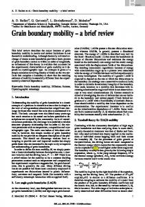
A Possible Solution of the Grain Boundary Problem for Applications of High-Tc Superconductors
arXiv:cond-mat/0208253v1 [cond-mat.supr-con] 13 Aug 2002
G. Hammerl, A. Herrnberger, A. Schmehl, A. Weber, K. Wiedenmann, C. W. Schneider, and J. Mannhart Experimentalphysik VI, Center for Electronic Correlations and Magnetism, Institute of Physics, Augsburg University, D-86135 Augsburg, Germany It is shown that the critical current density of high-Tc wires can be greatly enhanced by using a threefold approach, which consists of grain alignment, doping, and optimization of the grain architecture. According to model calculations, current densities of 4 · 106 A/cm2 can be achieved for an average grain alignment of 10◦ at 77 K. Based on this approach, a road to competitive high-Tc cables is proposed.
Vital for large scale applications of high-Tc superconductors [1,2] is the solution of the grain boundary problem, which manifests itself by the exponential decrease of the grain boundary critical current density Jc of the high-Tc cuprates as a function of the grain boundary angle [3,4]. We propose to solve this problem using a threefold approach: through 1) grain alignment [3], 2) grain boundary doping [5], and 3) optimization of the microstructure to maximize the effective grain boundary area [6]. In contrast to the powder-in-tube technology where large grain boundary areas and grain alignment are used to enhance Jc [7–9], today’s coated conductor technologies [10–12] focus on grain alignment only. As we have shown, however, simple ways exist to also preferentially dope the grain boundaries [5] and engineer large effective grain boundary areas [13,14] to further enhance the performance of coated conductors.
FIG. 1. Sketch of a coated conductor containing grains with big aspect ratios. Large currents are supported by the conductor, because bypasses around the standard, small area grain boundaries are provided.
The calculation of current percolation through disordered networks of weak links, some of which may be Josephson junctions, is a complex problem [6]; and several algorithms have been developed for its solution (see, e. g. Ref. 6, 15 – 19). As the fast algorithms are limited to two-dimensional networks, for the present work a new one had to be devised. Like in several of the existing algorithms, to achieve the required speed, phase effects and self fields were neglected.
As pointed out in 1987, large effective grain boundary areas can be realized by engineering the microstructure of the superconductor to obtain grains with big aspect ratios, for example by stacking in a brickwall-type manner platelet-like grains on top of each other [6,7]. The enhancement of the critical currents hereby gained is responsible for the large Jc of the Bi-based high-Tc superconductors fabricated with the powder-in-tube technology [6–9]. Recently we found ways to use large effective grain boundary areas to enhance Jc of coated conductors that consist of two- or three dimensional grain boundary networks, as illustrated in Fig. 1. Although it is clear that each one of the three techniques described substantially enhances Jc , the increase that can be gained by utilizing all three, for example as shown by Fig. 2, is unknown.
FIG. 2. Simplified sketch of a tape, fabricated by the rolling assisted biaxially textured substrate (RABiTS) technology, with a modified grain architecture which is based on grains with aspect ratios ρ ≫ 1. Preferentially doping of the grain boundaries is achieved by utilizing a doped cap layer and grain boundary diffusion.
Therefore we have calculated the performance, which can be achieved by combining grain orientation, doping, and large effective grain boundary areas. Based on these calculations, optimized sets of parameters for the fabrication of coated conductors are derived. 1
These calculations are based on Dijkstra’s shortest path algorithm for undirected graphs [20], the grains acting as vertices, the grain boundaries, weighted by their critical currents, as edges. To initialize a calculation, a polycrystalline superconductor, typically containing 103 – 104 grains is modelled first. To this superconductor an intragrain Jc,grain and misorientation angle dependent grain boundary critical current densities Jc = Jc (θ) are ascribed. The calculations are performed in steps, in each step i the algorithm finds in Dijkstra’s sense the shortest path through the network. The critical current Ii of this path and the respective current densities are calculated and compared to the current densities of the grains and boundaries that form this path. At the end of step i, the critical currents of the grains and grain boundaries involved are reduced by Ii . After the final step m, all possible current paths have been cancelled by this P procedure and the critical current I is given by I = m i=1 Ii . These calculations are repeated N times to calculate Jc for different networks. The final result is obtained by averaging the intermediate results. Because the algorithm uses an undirected graph model, it is fast and capable to determine the critical current of three dimensional grain boundary networks. Its accuracy is a function of the grain number and of N . The numerical accuracy of the data presented, typically obtained with 103 grains and N = 20, is better than 5%. This algorithm was used to assess possible approaches for the optimization of coated conductors at 77 K. For the present calculations, the intragrain Jc was taken to be 5 · 106 A/cm2 , and the grain orientations and lengths were chosen using Gaussian distributions with parameterized widths (see also Ref. 13). To determine the effects of doping on Ic the Jc (θ)-dependence in the simulation was modified based on the experimental data [5], which show that at least in the range of 24◦< θ < 36◦ the critical current density can be doubled by doping. For lower and higher angles, Jc is taken to be exponentially reduced to the undoped values. To consider the effects of stacking coated conductors in multilayer configurations, the intergrain critical currents flowing in c-direction were modelled by reducing Jc (θ) by an additional c-axis coupling factor fc . For bilayers, the transverse misalignment of the grains in the top and bottom layer was taken to be 30% of the grain width. These calculations provide a clear assessment of the possibilities to optimize coated conductors, as shown in the following. In Fig. 3 the critical current densities of various coated conductors are plotted as function of the average grain misorientation σ and aspect ratio ρ of the grains. As seen, the current density of conventional tapes (ρ = 1, σ ≥ 15◦ ) is approximately doubled by doping the grain boundaries, in agreement with experimental results. An enhancement of the aspect ratio significantly increases Ic further, and a tape with σ = 45◦ and ρ = 50 has the same Jc as conven-
tional tape with an alignment of 6◦ . This graph suggests to combine moderate grain alignment (σ = 10 ◦ ), large aspect ratios (ρ = 20 to 30), and doping to achieve critical current densities of 3 − 4 · 106 A/cm2 .
FIG. 3. Calculated critical current densities of various RABiTS tapes with different grain aspect ratios ρ as a function of the grain misorientation σ.
As revealed by Fig. 4, in which Jc is plotted as a function of aspect ratio ρ and coupling fc for two undoped RABiTS tapes with 10◦ texturing stacked on top of each other, the use of bilayers increases Jc roughly by 106 A/cm2 . Bilayers therefore only provide a significant advantage for conventional tapes with ρ ≈ 1. The benefits are much smaller for tapes with larger aspect ratios and it seems reasonable to apply for a given tape only either stacking or elongation of the grains.
FIG. 4. Calculated dependence of the critical current density as a function of the aspect ratio ρ of two RABiTS tapes with misorientation σ = 10◦ stacked on top of each other with different coupling factors fc = 0 (a), 10−4 (b), and 10−3 (c). The inset shows a sketch of such a tape, the intermediate layer is used to weld the two tapes together.
2
The perspectives opened by the data shown in Fig. 3 and Fig. 4 suggest the mass production of high-Tc tapes, as illustrated by Fig. 5.
duction of coated conductors with large critical currents. We gratefully acknowledge helpful discussions with M. Beasley, J. G. Bednorz, M. Blamire, P. Chaudhari, T. Claeson, J. Evetts, H. Hilgenkamp, B. Holzapfel, Z. G. Ivanov, S. Leitenmeier, D. G. Schlom, and L. Schultz. This work was supported by the BMBF (13N6918).
[1] J. G. Bednorz and K. A. M¨ uller, Z. Phys. B 65, 189 (1986). [2] M. K. Wu et al., Phys. Rev. Lett. 58, 908 (1987). [3] D. Dimos, P. Chaudhari, and J. Mannhart, Phys. Rev. B 41, 4038 (1990); Z. G. Ivanov et al., Appl. Phys. Lett. 59, 3030 (1991). [4] H. Hilgenkamp and J. Mannhart, Rev. Mod. Phys. 74, 485 (2002). [5] G. Hammerl et al., Nature 407, 162 (2000). [6] J. Mannhart and C. C. Tsuei, Z. Phys. B 77, 53 (1989). [7] J. Mannhart, ”What limits the critical current density in high-Tc superconductors?”, in Earlier and Recent Aspects of Superconductivity, edited by J. G. Bednorz and K. A. M¨ uller (Springer-Verlag, Heidelberg), 208 (1990). [8] L. N. Bulaevskii et al., Phys. Rev. B 45, 2545 (1992). [9] B. Hensel, G. Grasso, and R. Fl¨ ukiger, Phys. Rev. B. 51, 15456 (1995). [10] Y. Iijima et al., Appl. Phys. Lett. 60, 769 (1992). [11] D. P. Norton et al., Science 274, 755 (1996). [12] M. Bauer, R. Semerad, and H. Kinder, IEEE Trans. Appl. Supercond. 9, 1502 (1999). [13] S. Leitenmeier et al., Ann. Phys. (Leipzig) 11, 3 (2002). [14] G. Hammerl et al., Eur. Phys. J. B 27, 299 (2002). [15] C. S. Nichols and D. R. Clarke, Acta Metallurgica 39, 995 (1991). [16] Z.-X. Cai and D. O. Welch, Phys. Rev. B 45, 2385 (1992). [17] B. Hensel et al., Physica C 205, 329 (1993). [18] N. A. Rutter, B. A. Glowacki, and J. E. Evetts, Supercond. Sci. Technol. 13, L25 (2000); B. Zeimetz et al., Supercond. Sci. Technol. 14, 672 (2001). [19] B. Holzapfel et al., IEEE Trans. Appl. Supercond. 11, 3872 (2001). [20] E. Dijkstra, Numer. Math. 1, 269 (1959). [21] F. E. H. M¨ uller, M. Heilmaier, and L. Schultz, Mat. Science and Eng. 234, 509 (1997). [22] T. Araki et al., Supercond. Sci. Technol. 15, L1 (2002); Q. Li et al., Physica C 357–360, 987 (2001).
FIG. 5. Sketch illustrating large scale production of ReBa2 Cu3 O7−δ based RABiTS tapes as suggested by the results shown in Fig. 3 and 4.
This process is based on the standard RABiTS technology, and is aimed to generate tapes with high critical currents by utilizing grain boundary doping and tapes containing grains with big aspect ratios. Here it is envisaged that Ni tapes with elongated grains and proper texture can be fabricated, using processes as reported in Ref. 21. A RABiTS tape is rolled and annealed to obtain an average grain misorientation of ≈ 10◦ and aspect ratios in the range of 20 – 50. The buffer layer system and the ReBa2 Cu3 O7−δ -film are deposited with non-vacuum techniques [22], before the tape is covered with a cap layer of Re1−x Cax Ba2 Cu3 O7−δ , annealed and cut. According to Fig. 3, such tapes support critical current densities of 4 · 106 A/cm2 , corresponding to critical currents of 400 A/cm for 1 µm thick, single sided superconducting films. Although significant technological problems associated with the growth of thick superconducting films, ac-losses, and quench protection remain to be solved, the process outlined appears to be suited for large scale pro-
3