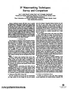
533
RADIOENGINEERING, VOL. 20, NO. 2, JUNE 2011
A Sequential Circuit-Based IP Watermarking Algorithm for Multiple Scan Chains in Design-for-Test Wei LIANG1,2,3, *Xingming SUN1,3, Zhiqiang RUAN1,3, Jing LONG2, Chengtao WU3 1
Jiangsu Engg. Center of Network Monitoring, Nanjing Univ. of Information Sci. & Technology, Nanjing, 210044, China 2 School of Computer Science and Engineering, Hunan University of Science and Technology, Xiangtan, 411201, China 3 School of Computer and Communication, Hunan University, Changsha, 410082, China
[email protected],
[email protected],
[email protected],
[email protected],
[email protected]
Abstract. In Very Large Scale Integrated Circuits (VLSI) design, the existing Design-for-Test(DFT) based watermarking techniques usually insert watermark through reordering scan cells, which causes large resource overhead, low security and coverage rate of watermark detection. A novel scheme was proposed to watermark multiple scan chains in DFT for solving the problems. The proposed scheme adopts DFT scan test model of VLSI design, and uses a Linear Feedback Shift Register (LFSR) for pseudo random test vector generation. All of the test vectors are shifted in scan input for the construction of multiple scan chains with minimum correlation. Specific registers in multiple scan chains will be changed by the watermark circuit for watermarking the design. The watermark can be effectively detected without interference with normal function of the circuit, even after the chip is packaged. The experimental results on several ISCAS benchmarks show that the proposed scheme has lower resource overhead, probability of coincidence Pc and higher coverage rate of watermark detection S by comparing with the existing methods.
Keywords IP reuse, VLSI, DFT, LFSR, multiple scan chains.
1. Introduction With the rapid development of deep sub-micron integrated circuit systems, SOC (System on Chip) has become the mainstream in IC (Integrated Circuit) design. IP (Intellectual Property) reuse used by more semiconductor companies is essential to shorten design time and reduce product risk [1-3]. The problem of effective IP protection has been widely concerned. Digital watermarking applied in DFT design has been extensively concerned [4], [5]. For most of the DFT watermarking techniques, the authors can insert their copyright into IP core, thus enabling identification of these cores. DFT watermarking, typically “protection and detection”, is an IP protection technique for embedding watermark at various design stage of SOC design by using testability.
Recently, a number of DFT watermarking techniques have been proposed [6-22]. In the methods proposed by Fan et al. [7-8], the watermark generation is integrated in the test module. Five possible methods for watermark hiding are presented. Since only the test circuit instead of the IP core is marked independently, it is vulnerable to removal attacks. Cui et al. [9-11] proposed to insert watermark through reordering the scan cells in a single scan chain minimizing power overhead. Saha et al. [12-13] proposed to watermark both the scan tree and single scan chain, separately embedding the signatures of the owner of physical design tool and that of the logic design tool. The scheme proposed by Kirovski [14-15] marked the design by restricting some specific registers to appear in the scan chain at the DFT stage. The watermark is verified by comparing some simulation values of the design and the retrieved values in the output vectors in the test mode. It is only applicable to the partial scan architectures but not full scan designs. These techniques solve the problems of watermark embedding time, additional overhead and traceability existed in the previous methods. However, with the increasing complexity of circuit, the correlation of test vector for multiple scan chains may affect the circuit performance. Moreover, these methods are vulnerable to reverse engineering attack. The attackers can damage the overall project only by resynthesis and remapping. An IP protection method is proposed by watermarking multiple scan chains in sequential circuit. The proposed scheme adopts DFT test model in SOC design, and uses an LFSR for pseudo random test vector generation [16]. All of the test vectors are shifted in scan input for the construction of multiple scan chains with minimum correlation. A watermark logic circuit is designed to change specific registers in multiple scan chains for watermarking the design.
2. Related Work Usually, digital watermarking [17-20] methods are used along with DFT design in practical application. In this section, some basic definitions lay out the theoretical foundation for the construction of multiple scan chains with the minimum correlativity.
534
WEI LIANG, ET AL., A SEQUENTIAL CIRCUIT-BASED IP WATERMARKING ALGORITHM FOR MULTIPLE SCAN CHAINS …
Definition 1: If there is at least one path from input vector SI to output vector SO in sequential circuit, SI is connected with SO. If there is at least one output vector SO connected with input vectors SI1 and SI2 respectively, then SI1 and SI2 are correlated; otherwise, uncorrelated. Definition 2: In sequential circuit, N output vectors connected with input vectors SI1 and SI2 respectively, if it exists, the correlation is N, denoted by (SI1, SI2) = N or (SI2, SI1) = N; otherwise, SI1 and SI2 are uncorrelated, (SI1, SI2) = 0 or (SI2, SI1) = 0. Definition 3: In multiple scan chains M, supposing each chain has equal length, denoted by d (except as hereinafter provided). The ordering of scan cells in c1 and c2 is represented by {s1,1, s1,2,…,s1,n} and {s2,1, s2,2,…,s2,m} respectively. The correlation of scan chains c1 and c2 is denoted by c1 , c2 : d
c1 , c2 s1,i , s2,i .
(1)
i 1
Similarly, in multiple scan chains M with λ scan chains c1, c2,…,cλ, correlation of M is the sum of correlation of every two different scan chains, denoted by M : 1
1
i 1 j i 1
i 1 j i 1 k 1
d
d
M ci , c j si,k , s j ,k (k ) . 1
Here, (k )
i 1 j i 1
(2)
k 1
si,k , s j ,k denotes the sum of correla-
tion of every two different input signals in column k of the multiple scan chains. Definition 4: In multiple scan chains M, considering two input signals s ,k , s ,k2 respectively in columns k1, k2, if the inequation 1
k1
s
i1,i
i,k1
k2
s
, s,k 2
i1,i
i,k 2
k1
s
, s,k1
i,k1
i1,i
k2
s
, s,k1
i,k2
i1,i
, s,k 2 (3)
is satisfied, that is , , , where k1 k2 1, d , 1, k1 and 1,| k2 | , then s ,k1 and s ,k2 is exchangeable, the exchange operation is called vector exchange. k1
k2
k1
k2
Theorem: Multiple scan chains M0 is transformed into Mp after series of vector exchanges. In multiple scan chains Mp, two input signals s ,k1 , s ,k2 in any two columns k1 and k2, the inequation
k1
k2
,
,
k1
k2
is satisfied,
where k1 k2 1, d , 1, k1 , 1, k2 . There-
fore, correlation of the multiple scan chains Φ(Mp) is the minimum. Proof: Consider M0, if any two input signals in any two columns satisfy the inequation in theorem, M0 is equal to Mp; otherwise, there must be at least two input signals in different columns not satisfying the inequation. Randomly selecting two input signals P and Q, P in column ki and Q in k k k k column kj, ki k j 1, d , P ,Q P ,Q P Q , the i
j
i
j
vector correlation of M0 is defined as: M 0 ki k j
d
k
(4)
k 1, k ki , k k j
P Q u m ki
kj
u is constant uncorrelated with P and Q, m represents vector correlation sum of other columns except ki and kj. By exchanging the positions of P and Q in M0, we get multiple scan chains M1. In Φ(M1), the correlation of the vectors has no change except that of columns ki and kj, thus we have M 1 ki1 k j1
d
k
(5)
k 1, k ki , k k j
P ,Q Q , P u m ki
kj
Comparing (4) and (5), since have Φ(M1) < Φ(M0).
ki P
Q P ,Q Q , P , we kj
ki
kj
We perform the same operations on M1. Considering M1, if any two input signals in any two columns satisfy the inequation, M1 is equal to Mp; otherwise, perform another exchange for new multiple scan chains M2, having Φ(M2) < Φ(M1), repeat by the same logic. Considering multiple scan chains Mp, any two input signals s ,k1 , s ,k2 in any two columns k1 and k2,
k1
k2
,
,
k1
k2
is satis-
fied. If k1 is equal to k2, the correlation Φ(Mp) will not be affected after exchanging positions; otherwise, the correlation of the new multiple scan chains after exchanging positions must be equal or greater than Φ(Mp). Thus the vector correlation of multiple scan chains Mp denoted by Φ(Mp) is the minimum. Simultaneously, correlation of vectors in new multiple scan chains decreases a positive integer after an exchange operation. Therefore, for any design with multiple scan chains architecture, the minimum correlation must be equal or greater than 0, i.e. multiple scan chains M0 will be transformed into Mp after finite times of exchange operations and Mp has the minimum correlation.
3. Multiple Scan Chains-Based Watermarking 3.1 Watermarking Principle The test architecture of multiple scan chains has emerged for solving the test time problem in single scan chain [21]. Here, architecture of multiple scan chains with the minimum correlation is presented for better performance. The multiple scan chains Md could be transformed into Mp with the minimum correlation Φ(Mp) after exchange operations. Fig. 1 shows the test architecture of multiple scan chains. LFSR shifts test vectors in multiple scan chains for testing. By comparing with single scan chain, multiple scan chains architecture has the advantage of less test time and good resistance.
535
RADIOENGINEERING, VOL. 20, NO. 2, JUNE 2011
In the normal mode (w_en=0), the circuit under test executes normal scan test and in the watermark mode (w_en=1), a specific state shifted in ALC may cause 1, thus values of some cells in multiple scan chains will be reversed and then be output. The IP identification could be verified by comparing the output in normal mode and watermark mode for the same input vector.
3.2 Watermark Embedding
Fig. 1. The test architecture of multiple scan chains.
Fig. 2 shows the watermarking architecture of multiple scan chains in DFT. LFSR provides test vectors for n chains and input of watermark circuit (WMC). After watermarking, the watermarked response vectors will be shifted out.
First of all, the signature, which can intuitively represent one’s identity, is encrypted and then hashed [22]. The generated digital digest is inserted into IP core as watermark. Hash function H is actually a transformation, using x as input, the returned value is called hash value, denoted by h, i.e. h = H(x). Since hash is an oneway function, given a value h, it is impossible to calculate x by using H(x) = h. Assume that, the signature is “hnulw…”, firstly, we transform it into ASCII code “110100011…”. The RSA algorithm is used for encryption, with the encrypted text denoted by W. By using hash function H, the digital digest Msg = H(W) is generated, i.e. the watermark Wm. After that, we generate a random sequence without repetition, represented by Rn = {r1, r2,…,rn}. With the sequence, the watermark Wm will be grouped into a number of fragments, denoted by wm , wm ,..., wm . These fragments are mapped into a set of position constraints for watermark embedding. 1
2
Group sequence:
Watermark sequence: 1 0 0
Fig. 2. The watermarking architecture of multiple scan chains.
Fig. 3 shows an example for watermarking multiple scan chains. Assume that, the circuit under test consists of 6 scan cells si , i = 1, 2,…,6, these cells are organized into two scan chains c1 = {s1,s2,s3} and c2 = {s4,s5,s6}. In the watermark circuit, one input of XOR gate is connected to one cell in multiple scan chains, and another controlled by watermark enable signal w_en and output of arbitration logic circuit (ALC). However, the output of ALC is under the control of states in LFSR.
Embedded positions:
of
multiple
scan
chains
based
4
2
4
…
11
0101
…
3
6
…
Fig. 4. The generation of watermark fragments.
Suppose that the generated digital digest Msg =100110101…, i.e. the watermark Wm. The random sequence Rn = {3, 2, 4…} is used to group watermark into fragments, the numbers in Rn represent the length of each watermark fragment wm (i = 1,2,…,λ). As shown in Fig. 4, i after grouping, the first three watermark fragments are wm1 100 , wm 2 11 , wm 3 0101 , and the corresponding decimal numbers are respectively 4, 3, 6. This sequence represents the positions of the watermarked registers. The specific registers at these positions will be changed through watermark circuit for watermarking. The following pseudo-code summarized the approach: Read in netlist and desired signature S; WA CHAR _ TO _ ASCII ( S ) ; WAR (WA ) ; Wm H (WAR ) , store Wm; Generating random sequence Rn(k) = Random(), store Rn(k); 6 Rn(k): Group (Wm); 7 for(i=1; group number i