Jun 28, 2007 - 2QUANTOP, Danish Quantum Optics Center and Niels ... realization of remarkable nonlinear optical phenomena, where individual photons strongly ..... The key principle is to utilize the presence or absence of a photon in an initial âgateâ pulse ..... [28] Shen, J.T. & Fan, S. Coherent photon transport from ...
A single-photon transistor using nano-scale surface plasmons D.E. Chang,1 A.S. Sørensen,2 E.A. Demler,1 and M.D. Lukin1 1
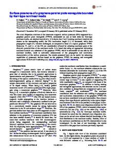
Physics Department, Harvard University, Cambridge, MA 02138 2
QUANTOP, Danish Quantum Optics Center and Niels
arXiv:0706.4335v1 [quant-ph] 28 Jun 2007
Bohr Institute, DK-2100 Copenhagen Ø, Denmark (Dated: February 1, 2008)
Abstract It is well known that light quanta (photons) can interact with each other in nonlinear media, much like massive particles do, but in practice these interactions are usually very weak. Here we describe a novel approach to realize strong nonlinear interactions at the single-photon level. Our method makes use of recently demonstrated efficient coupling between individual optical emitters and tightly confined, propagating surface plasmon excitations on conducting nanowires. We show that this system can act as a nonlinear two-photon switch for incident photons propagating along the nanowire, which can be coherently controlled using quantum optical techniques. As a novel application, we discuss how the interaction can be tailored to create a single-photon transistor, where the presence or absence of a single incident photon in a “gate” field is sufficient to completely control the propagation of subsequent “signal” photons.
1
In analogy with the electronic transistor, a photonic transistor is a device where a small optical “gate” field is used to control the propagation of another optical “signal” field via a nonlinear optical interaction [1, 2]. Its fundamental limit is the single-photon transistor, where the propagation of the signal field is controlled by the presence or absence of a single photon in the gate field. Nonlinear devices of this kind would have a number of interesting applications ranging from optical communication and computation [2] to quantum information processing [3]. However, their practical realization is challenging because the requisite single-photon nonlinearities are generally very weak [1]. While several schemes for producing nonlinearities at the single-photon level are currently being explored, ranging from resonantly enhanced nonlinearities of atomic ensembles [4, 5, 6, 7, 8] to individual atoms strongly coupled to photons in cavity quantum electrodynamics (QED) [9, 10, 11, 12, 13], a robust, practical approach has yet to emerge. Recently, a new method to achieve strong coupling between light and matter has been proposed [14] and experimentally demonstrated [15]. It makes use of the tight concentration of optical fields associated with guided surface plasmons (SPs) on conducting nanowires to achieve strong interaction with individual optical emitters. In essence, the tight localization of these fields causes the nanowire to act as a very efficient lens that directs the majority of the spontaneously emitted light into the SP modes, resulting in efficient generation of single plasmons (single photons) [14]. While this process is essentially a linear optical effect, as it only involves one photon at a time, here we show that such a system also allows for the realization of remarkable nonlinear optical phenomena, where individual photons strongly interact with each other. As an example, we describe how these nonlinear processes may be exploited to implement a single-photon transistor. While ideas for developing plasmonic analogues of electronic devices by combining SPs with electronics are already being explored [16], the process we describe here opens up fundamentally new possibilities, in that it combines the ideas of plasmonics with the tools of quantum optics [5, 7, 8, 10] to achieve unprecedented control over the interactions of individual light quanta.
NANOWIRE PLASMONS: INTERACTION WITH MATTER
SPs are propagating electromagnetic modes confined to the surface of a conductordielectric interface [16, 17]. Their unique properties make it possible to confine them to 2
sub-wavelength dimensions, which has led to fascinating new approaches to waveguiding below the diffraction limit [18], enhanced transmission through sub-wavelength apertures [19], and sub-wavelength imaging [20, 21, 22]. Large field enhancements associated with plasmon resonances of metallic nano-particles have also been utilized to detect nearby single molecules via surface-enhanced Raman scattering [23, 24]. Similar properties directly give rise to the strong interaction between single SPs on a conducting nanowire and an individual, proximal optical emitter (see Figs. 1a, b), as we describe below. Much like in a single-mode fiber, the SP modes of a conducting nanowire constitute a one-dimensional, single-mode continuum that can be indexed by the wavevectors k along the direction of propagation [14, 18, 25]. Unlike a single-mode fiber [26], however, the nanowire continues to display good confinement and guiding when its radius is reduced well below the optical wavelength (R≪λ0 ). Specifically, in this limit, the SPs exhibit strongly reduced wavelengths and small transverse mode areas relative to free-space radiation, which scale like λpl ∝1/k∝R and Aeff ∝R2 , respectively. The tight confinement results in a large interaction strength between the SP modes and any proximal emitter with a dipole-allowed transition, √ with a coupling constant that scales like g ∝ 1/ Aeff . The reduction in group velocity also yields an enhancement of the density of states, D(ω) ∝ 1/R. The spontaneous emission rate into the SPs, Γpl ∼g 2 (ω)D(ω) ∝ (λ0 /R)3 , can therefore be much larger than the emission
rate Γ′ into all other possible channels. A relevant figure of merit is an effective Purcell
factor P ≡ Γpl /Γ′ , which can exceed 103 in realistic systems (see Fig. 1c). As will be seen, the Purcell factor plays an important role in determining the strength and fidelity of the nonlinear processes of interest. Motivated by these considerations, we now describe a general one-dimensional model of an emitter strongly coupled to a set of travelling electromagnetic modes (see Figs. 1a, b). We first consider a simple two-level configuration for the emitter, consisting of ground and excited states |gi, |ei separated by frequency ωeg . The Hamiltonian describing this system is given by H=h ¯ (ωeg − iΓ′ /2)σee +
Z
dk h ¯ c|k|ˆ a†k a ˆk − h ¯g
Z
�
�
dk σeg aˆk eikza + h.c. ,
(1)
where σij = |iihj|, a ˆk is the annihilation operator for the mode with wavevector k, g is the emitter-field interaction matrix element, and za is the position of the emitter. We have assumed that a linear dispersion relation holds over the relevant frequency range, νk = c|k|, 3
where c is the group velocity of SPs on the nanowire, and similarly that g is frequencyindependent. In the spirit of the stochastic wave function or “quantum jump” description of an open system [27], we have also included a non-Hermitian term in H due to the decay of state |ei into a reservoir of other radiative and non-radiative modes at a rate Γ′ . SINGLE EMITTER AS A SATURABLE MIRROR
The propagation of SPs can be dramatically altered by interaction with the single twolevel emitter. In particular, for low incident powers, the interaction occurs with near-unit probability, and each photon can be reflected with very high efficiency. At the same time, for higher powers the emitter response rapidly saturates, as it is not able to scatter more than one photon at a time. The low-power behavior can be easily understood by first considering the scattering of a single photon, as illustrated schematically in Fig. 1b. Since we are interested only in SP modes near the optical frequency ωeg , we can effectively treat left- and right-propagating SPs as completely separate fields. In particular, one can define operators that annihilate √ R a left (right)-propagating photon at position z, EˆL(R) (z) = (1/ 2π) dk eikz a ˆL(R),k , where operators acting on the left and right branches are assumed to have vanishing commutation relations with the other branch. An exact solution to the scattering from the right to left branches in the limit P → ∞ was derived in [28], and this approach can be generalized to finite P . In particular, it is possible to solve for the scattering eigenstates of a system containing at most one (either atomic or photonic) excitation, as described in Methods. The reflection coefficient for an incoming photon of wavevector k is r(δk ) = −
1+
Γ′ /Γ
1 , pl − 2iδk /Γpl
(2)
where δk ≡ck−ωeg is the photon detuning, while the transmission coefficient is related to r by
t(δk ) = 1+r(δk ). Here Γpl = 4πg 2 /c is the decay rate into the SPs, as obtained by application of Fermi’s Golden Rule to the Hamiltonian in Eq. (1). On resonance, r≈ − (1 − 1/P ), and
thus for large Purcell factors the emitter in state |gi acts as a nearly perfect mirror, which simultaneously imparts a π-phase shift upon reflection. The bandwidth ∆ω of this process is determined by the total spontaneous emission rate, Γ = Γpl + Γ′ , which can be quite large. Furthermore, the probability κ of losing the photon to the environment is strongly 4
suppressed for large Purcell factors, κ≡1 − R − T = 2R/P , where R (T ) ≡ |r|2 (|t|2 ) is the reflectance (transmittance). These results are illustrated in Fig. 1d, where R, T , κ are plotted as a function of detuning δk , taking a conservative value of P = 20. The nonlinear response of the system can be seen by considering the interaction of a single emitter not just with a single photon, but with multi-photon input states. While the reflectance and transmittance for this system at low powers resemble those derived for a single photon, the arrival of several photons within the bandwidth ∆ω∼Γ saturates the atomic response and these photons cannot be efficiently reflected. To be specific, we consider the case when the incident field consists of a coherent state, the quantum mechanical state that most closely corresponds to a classical field [27]. We now describe a mapping that allows the scattering dynamics to be solved exactly. We assume that the incident field propagates to the right and that the emitter is initially in the ground state, such that the ˜ initial wave function can be written in the form |ψ(t→ − ∞)i = D({αk e−iνk t })|vaci|gi, where the displacement operator D({αk }) ≡ exp( dk aˆ†R,k αk − αk∗ aˆR,k ) [27] creates a multiR
mode coherent state from vacuum. This property of the displacement operator motivates a state transformation given by [29] ˜ = D {αk e−iνk t } |ψi, |ψi �
�
(3)
so that the initial state is transformed into |ψ(t→ − ∞)i = |vaci|gi. In the Heisenberg picture, the field operator transforms as EˆR (z, t)→EˆR (z, t) + Ec (z, t), where the external field √ R amplitude is Ec (z, t) = (1/ 2π) dk αk eikz−iνk t . The transformation thus maps the initial
coherent state to a c-number in the interaction Hamiltonian, which physically corresponds to √ a classical Rabi frequency (given by Ωc = 2πgEc ), while simultaneously mapping the initial photonic state to vacuum. An important consequence is that the dynamics of the emitter interacting with the field modes can now be treated under the Wigner-Weisskopf approximation, i.e., interaction with the vacuum modes gives rise to an exponential decay rate from state |ei to |gi at a rate Γ. The evolution of the atomic operators consequently reduces to the usual Langevin-Bloch equations [27], which enables all properties of the atomic operators and the scattered field to be calculated (see Methods). For a narrow bandwidth (δω≪Γ), resonant (δk = 0) input field, the steady-state transmittance and reflectance are found to be T =
1 + 8(1 + P )2 (Ωc /Γ)2 , (1 + P )2 (1 + 8(Ωc /Γ)2 ) 5
(4)
R =
1 1+ P
�
�−2
1 . 1 + 8(Ωc /Γ)2
(5)
At low powers (Ωc /Γ≪1), the emitter has scattering properties identical to the single-photon case, R≈(1 + 1/P )−2 , T ≈(1 + P )−2 , and for large Purcell factors the single emitter again acts as a perfect mirror. At high incident powers (Ωc /Γ≫1), however, the single emitter saturates and most of the incoming photons are simply transmitted past with no effect, T →1, R∼O((Γ/Ωc )2 ). The significance of these results can be understood by noting that saturation is achieved at a Rabi frequency Ωc ∼ Γ that, in the limit of large P , corresponds to a switching energy of a single quantum (∼ h ¯ ν) within a pulse of duration ∼ 1/Γ. PHOTON CORRELATIONS
The strongly nonlinear atomic response at the single-photon level leads to dramatic modification of photon statistics that cannot be captured by only considering average intensities. We now consider higher-order correlations of the transmitted and reflected fields. Specifically, we focus on the normalized second-order correlation function for the outgoing field, (2)
gR,L (t), which for a stationary process is defined as (2) ˆ † (z, τ )Eˆ † (z, τ + t)Eˆβ (z, τ + t)Eˆβ (z, τ )i/hE ˆ † (z, τ )Eˆβ (z, τ )i2 , gβ=R,L (z, t) ≡ hE β β β
(6)
where t denotes the difference between the two observation times τ and τ + t. The statistics of the reflected field is identical to the well-known result for resonance fluorescence [27] in three dimensions (see Fig. 2). This can intuitively be understood because it is a purely scattered field. It follows that the field is strongly anti-bunched, g (2) (0) = 0, since the emitter can only absorb and re-emit one photon at a time. The transmitted field, however, has unique properties because it is a sum of the incident and scattered fields. For near-resonant excitation, we find for low powers that (see Methods) �
g (2) (t) = e−Γt P 2 − eΓt/2
�2
+ O(Ω2c /Γ2 ),
(7)
while for high powers g (2) (t) approaches unity for all times. The high power result indicates that no change in statistics occurs and is due to saturation of the atomic response. The low-power behavior reflects that of an efficient single-photon switch. In particular, for P ≫1, individual photons have a large reflection probability, but when two photons are incident 6
simultaneously the transition saturates, so that photon pairs have a much larger probability of transmission (for P ≪1 the emitter has little influence and the statistics of the transmitted field are almost unchanged). This phenomenon yields a strong bunching effect at t = 0 that behaves like g (2) (0)≈P 4 . One also finds a subsequent anti-bunching and perfect vanishing of g (2) (t) at the later time t0 = (4 log P )/Γ for weak input fields. A more detailed understanding of these features can be gained from a quantum jump picture describing the system’s evolution following the detection of a photon [30]. Unlike for the reflected field, the picture for the transmitted field is more complicated because one cannot determine whether the detected photon originates from the emitter or from direct transmission of the incident field. More formally, the change in the wave function following detection is described by the application of a jump operator to the system, given in this case by the √ ˆT = EˆR,f ree + Ec + 2πigσge /c (cf. Eq. (10) in Methods). For transmitted field operator, E ˆT is strongly influenced by its atomic component. This is responsible for, e.g., large P , E the low transmittance T ≈(1 + P )−2 in steady-state, as the field scattered by the emitter destructively interferes with the incoming field. Because multiple incident photons increase the transmission probability, the detection of a photon enhances the conditional probability that another photon is present in the system. In the quantum jump picture this translates into a sudden enhancement of the coherence hσge i by a factor of 1 + P over its steady-state value (see Methods). The destructive interference between the incoming and scattered fields ˆT i is subsequently lost, and the jump causes a sudden enhancement in the field amplitude hE while also inducing a π-phase shift relative to its equilibrium value. The initial enhancement ˆT i gives rise to bunching. Then, the π-phase shift and subsequent relaxation back to in hE
equilibrium causes hEˆT i to pass through zero at time t0 , which yields the subsequent anti-
bunching and reflects the cancellation of the incoming and scattered fields. For P = 1, this cancellation happens exactly at t = 0 such that g (2) (0) = 0.
IDEAL SINGLE-PHOTON TRANSISTOR
While the two-level emitter analyzed previously is capable of acting as a switch that distinguishes between single- and multi-photon fields, a greater degree of coherent control can be gained by considering the interaction of light with a multi-level emitter. For concreteness, we consider the three-level configuration shown in Fig. 3. Here, a metastable state |si is 7
decoupled from the SPs due to, e.g., a different orientation of its associated dipole moment, but is resonantly coupled to |ei via some classical, optical control field with Rabi frequency Ω(t). States |gi, |ei remain coupled via the SP modes as discussed earlier. Using this system, we now describe a process in which a single “gate” photon can completely control the propagation of subsequent “signal” pulses consisting of either individual or multiple photons, whose timing can be arbitrary. In analogy to the electronic counterpart, this corresponds to an ideal single-photon transistor. We first describe how one can achieve coherent storage of a single photon, and then how this can be combined with the reflective properties derived above to realize a single-photon transistor. The storage is an important ingredient, as it provides an atomic memory of the gate field and hence allows the gate to interact with the subsequent signal field. The idea behind single-photon storage is to initialize the emitter in |gi and to apply the control field Ω(t) simultaneous with the arrival of a single photon in the SP modes. The control field, if properly chosen (or “impedance-matched”) [31], will result in capture of the incoming single photon while inducing a spin flip from |gi to |si. Generally, one can show by time reversal symmetry [32] that the optimal storage strategy is the time-reversed process of single-photon generation, where the emitter is driven from |si to |gi by the external field while emitting a single photon, whose wavepacket depends on Ω(t). By this argument, it is evident that optimal storage is obtained by splitting the incoming pulse and having it incident from both sides of the emitter simultaneously (see Fig. 3), and that there is a one-to-one correspondence between the incoming pulse shape and the optimal field Ω(t). Moreover, the storage efficiency is identical to that of single photon generation and is thus given by ∼1 − 1/P for large P [14]. This result is also derived explicitly in Supplemental Information, where we solve for the dynamics of this three-level system exactly. Physically, the fidelity of storage is simply determined by the degree to which coupling of the emitter to the SP modes exceeds the coupling to other channels. A detailed analysis reveals that this optimum is achievable for any input pulse of duration T ≫1/Γ and for a certain class of pulses of duration T ∼ 1/Γ [32]. Finally, we note that if no photon impinges upon the emitter, the pulse Ω(t) has no effect and the emitter remains in state |gi for the entire process. The result is more generally described as a mapping between single SP states and metastable atomic states, (α|0i + β|1i)|gi → |0i(α|gi + β|si). We next consider the reflection properties of the emitter when the control field Ω(t) is 8
turned off. If the emitter is in |gi, the reflectance and transmittance derived above for the two-level emitter remain valid. On the other hand, if the emitter is in |si, any incident fields will simply be transmitted with no effect since this state is decoupled from the SPs. Therefore, with Ω(t) turned off, the three-level system effectively behaves as a conditional mirror whose properties depend sensitively on its internal state. The techniques of state-dependent conditional reflection and single-photon storage can be combined to create a single-photon transistor, whose operation is illustrated in Fig. 3. The key principle is to utilize the presence or absence of a photon in an initial “gate” pulse to conditionally flip the internal state of the emitter during the storage process, and to then use this conditional flip to control the flow of subsequent “signal” photons arriving at the emitter. The first step is to implement the storage protocol for the gate pulse, consisting of either zero or one photon, starting with the emitter in |gi. The presence (absence) of a photon causes the emitter to flip to (remain in) state |si (|gi). Next, the interaction of each signal pulse arriving at the emitter depends sensitively on the internal state that results after storage. The storage step and conditional spin flip causes the emitter to be either highly reflecting or completely transparent depending on the gate, and the system therefore acts as an efficient switch or transistor for the subsequent signal field. The ideal operation of the transistor is limited only by the characteristic time over which an undesired spin flip can occur. In particular, if the emitter remains in |gi after storage of the gate pulse, the emitter can eventually be optically pumped to |si upon the arrival of a sufficiently large number of photons in the signal field. For strong coupling the number of incident photons n that can be scattered before pumping occurs is given by the branching ratio of decay rates from |ei to these states, n∼Γe→g /Γe→s , which can be large due to the >P and the emitter can reflect O(P ) photons before large decay rate Γe→g ≥ Γpl . Thus n∼ an undesired spin flip occurs. This number corresponds to the effective “gain” of the singlephoton transistor. Finally, we note that there exist other possible realizations of a single-photon transistor as well. The “impedance-matching” condition and the need to split a pulse for optimal storage, for example, can be relaxed using a small ensemble of emitters and photon storage techniques based on electromagnetically induced transparency (EIT) [33]. Here, storage also results in a spin flip within the ensemble that sensitively alters the propagation of subsequent photons. 9
INTEGRATED SYSTEMS
Thus far we have not dealt with the inevitable losses that SPs experience as they propagate along the nanowire, which could potentially limit their feasibility as long-distance carriers of information and their use in large-scale devices. For the nanowire, one must consider the trade-off between the larger Purcell factors obtainable with smaller diameters and a commensurate increase in dissipation due to the tighter field confinement. However, these limitations are not fundamental, if one can integrate SP devices with low-loss dielectric waveguides and other microphotonic devices. Here, the SPs can be used to achieve strong nonlinear interactions over very short interaction distances, but are rapidly in- and out-coupled to conventional waveguides for long-distance transport. One such integration scheme is illustrated in Fig. 4, where excitations are transferred to and from the SP modes of a nanowire from an evanescently coupled, phase-matched dielectric waveguide. The losses will be small provided that the distance needed for the SPs to be coupled in and out and interact with the emitter is smaller than the characteristic dissipation length. This can be accomplished by techniques such as optimizing of SP geometries (e.g., tapered wires or nanotips [14, 25]) and engineering of SP dispersion relations [34] via periodic structures. Coupling efficiencies exceeding 95%, for example, are predicted using simple systems [25]. Such a conductor/dielectric interface would provide convenient integration with conventional optical elements, enable many nonlinear operations without loss, and make large-scale, integrated photonic devices feasible. Another key feature of nano-scale SPs is that the strong interaction with a single emitter is very robust. In particular, the large coupling occurs over a very large bandwidth and no special tuning of either the emitter or nanowire is required. SPs are thus promising candidates for use with solid-state emitters such as quantum dot nanocrystals [35] or color centers [36], where the spectral properties can vary over individual emitters. Color centers in diamond [37], for instance, are especially promising because they offer sharp optical lines and three-level internal configurations. At the same time, guided SPs might be used for trapping isolated neutral atoms in the vicinity of suspended wires, thereby creating an effective interface for isolated atomic systems.
10
OUTLOOK
We now outline some new directions opened up by this work. We have shown that a single emitter near a conducting nanowire provides a strong optical nonlinearity at the level of single photons, which can be exploited to create a single-photon transistor. This can be used for a variety of important applications, such as very efficient single-photon detection, where the large gain in the signal field provides for efficient detection of the gate pulse. This system also finds applications in quantum information science. One can prepare Schrodinger cat states of photons, for example, if the gate pulse contains a superposition of zero and one photon, since this initial pulse can be entangled with the propagation direction of a large number of subsequent signal photons. The controlled-phase gate for photons proposed in [11] for cavity QED is also directly extendable to our plasmonic system. In particular, this scheme relies on the conditional phase shifts acquired as photons are reflected from a resonant cavity containing a single atom, which are analogous to the reflection dynamics derived for single SPs here. In addition, by using SPs it is possible to achieve very large optical depths with just a few emitters, which would make this system effective for realizing EIT-based nonlinear schemes [38]. Furthermore, the present system is an intriguing candidate to observe phenomena associated with strongly interacting, one-dimensional many-body systems. For example, non-perturbative effects such as photon-atom bound states [39] and quantum phase transitions [40] involving photons can be explored. Higher-order correlations created in the transmitted field can become a useful tool to study and probe the non-equilibrium quantum dynamics of these strongly interacting photonic systems.
METHODS Single-photon dynamics
Because we are interested only in the dynamics of near-resonant photons with an emitter, we can make the approximation that left- and right-propagating photons form completely separate quantum fields [28]. We define annihilation and creation operators for the two fields, aˆL(R),k , a ˆ†L(R),k , where the index k is assumed to run over the range ±∞; in principle this allows for the existence of negative-energy modes, but this is unimportant if we consider near-resonant dynamics. Under this two-branch approximation, the relevant terms in Eq. (1) 11
are transformed via σeg (ˆ aR,k + a ˆL,k ) eikza .
R
dk h ¯ c|k|ˆ a†k a ˆk →
R
�
dk h ¯ ck a ˆ†R,k a ˆR,k + aˆ†L,−k a ˆL,−k
�
and σeg a ˆk eikza →
To solve for the reflection and transmission coefficients of single-photon scattering, we write the general wave function for a system containing one (either photonic or atomic) excitation in the following way (here a two-level emitter is assumed), |ψk i =
Z
�
�
dz φL (z)EˆL† (z) + φR (z)EˆR† (z) |g, vaci + ce |e, vaci.
(8)
The field amplitudes are chosen to correspond to photons of well-defined momenta in the limits z→ ± ∞, e.g., φR (z→ − ∞)∼eikz , φR (z→∞)∼teikz , and φL (z → −∞) ∼ re−ikz for a photon propagating initially to the right, where t (r) is the transmission (reflection) coefficient. Following [28], we obtain Eq. (2) by solving the time-independent Schrodinger equation H|ψk i = Ek |ψk i for r, t and ce . Multi-photon dynamics
In the two-branch approximation, the Heisenberg equations of motion for the fields are given by !
1∂ ˆ ∂ ER (z, t) = + ∂z c ∂t
√
2πig σge (t)δ(z − za ), c
(9)
which can be formally integrated to give ˆR (z, t) = EˆR,f ree (z − ct) + E
√
2πig σge (t − (z − za )/c) Θ(z − za ), c
(10)
ˆL . Assuming that where Θ(z) is the Heaviside step function. A similar equation holds for E the field initially propagates to the right, EˆR (z, t) is the field transmitted past the emitter for z > za , while for z < za , EˆL (z, t) is the reflected field. We now discuss how to calculate the transmitted field intensity (a similar method holds for finding the reflected intensity). Under the transformation given by Eq. (3), the first-order correlation function for the right-going field is given by (1) GR (z, t) = h(EˆR† (z, t) + Ec∗ (z, t))(EˆR (z, t) + Ec (z, t))i,
(11)
which upon evaluating at z > za yields the average transmitted intensity. We proceed by substituting Eq. (10) into Eq. (11). Because the initial photonic state is vacuum following the transformation, EˆR,f ree has no effect and thus calculation of G(1) reduces to calculating 12
correlations between atomic operators. Techniques for evaluating these correlations are wellknown using the Langevin-Bloch equations [27]. Calculation of g (2) (t) proceeds in a similar manner by using Eq. (10) to express g (2) (t) in terms of two-time atomic correlations, which can be evaluated using the well-known quantum regression theorem [27]. The system in consideration undergoes a quantum jump following detection of a transmitted photon. Immediately following the detection, the density matrix is given by ˆT† /hE ˆT† EˆT i , where ρss is the steady-state density matrix and hi denotes ρjump = EˆT ρss E ss ss ˆT is the jump operator defined in the the average of quantities in steady state. Here E “Photon correlations” section and physically corresponds to the transmitted field. In the weak-field limit, it is straightforward to show that hσge ijump = (1 + P )hσge iss = 2iΩc /Γ′ , ˆT i = 1 − P 2 . Note in particular that for large P , there is an initial enand hEˆT ijump /hE ss hancement in the transmitted field amplitude as well as a π-phase shift from its equilibrium value.
[1] Boyd, R.W. Nonlinear Optics (Academic Press, New York, 1992). [2] Gibbs, H.M. Optical bistability: controlling light with light (Academic Press, Inc., Orlando, FL 1985). [3] Bouwmeester, D., Ekert, A. & Zeilinger, A., Eds. The Physics of Quantum Information (Springer, Berlin, 2000). [4] Schmidt, H. & Imamoglu, A. Giant Kerr nonlinearities obtained by electromagnetically induced transparency. Opt. Lett. 21, 1936 (1996). [5] Harris, S.E. Electromagnetically Induced Transparency. Phys. Today 50, 36 (1997). [6] Harris, S.E. & Yamamoto, Y. Photon Switching by Quantum Interference. Phys. Rev. Lett. 81, 3611 (1998). [7] Lukin, M.D. Colloquium: Trapping and manipulating photon states in atomc ensembles. Rev. Mod. Phys. 75, 457 (2003). [8] Fleischhauer, M., Imamoglu, A. & Marangos, J.P. Electromagnetically induced transparency: Optics in coherent media. Rev. Mod. Phys. 77, 633 (2005). [9] Vahala, K., Ed. Optical Microcavities (World Scientific, Singapore, 2004). [10] Miller, R. et al. Trapped atoms in cavity QED: coupling quantized light and matter. J. Phys.
13
B: At. Mol. Opt. Phys. 38, S551 (2005). [11] Duan, L.-M. & Kimble, H.J. Scalable Photonic Quantum Computation through CavityAssisted Interactions. Phys. Rev Lett. 92, 127902 (2004). [12] Birnbaum, K.M. et al. Photon blockade in an optical cavity with one trapped atom. Nature 436, 87 (2005). [13] Waks, E. & Vuckovic, J. Dipole Induced Transparency in drop filter cavity-waveguide systems. Phys. Rev. Lett. 96, 153601 (2006). [14] Chang, D.E., Sørensen, A.S., Hemmer, P.R. & Lukin, M.D. Quantum Optics with Surface Plasmons. Phys. Rev. Lett. 97, 053002 (2006). [15] Akimov, A.V. et al., submitted to Nature (2007). [16] Atwater, H.A. The promise of plasmonics. Scientific American 296, 56 (2007). [17] Maier, S.A. Plasmonics: fundamentals and applications (Springer-Verlag, New York, 2006). [18] Takahara, J., Yamagishi, S., Taki, H., Morimoto, A. & Kobayashi, T. Guiding of a onedimensional optical beam with nanometer diameter. Opt. Lett. 22,475 (1998). [19] Genet, C. & Ebbesen, T.W. Light in tiny holes. Nature 445, 39 (2007). [20] Klimov, V.V., Ducloy, M. & Letokhov, V.S. A model of an apertureless scanning microscope with a prolate nanospheriod as a tip and an excited molecule as an object. Chem. Phys. Lett. 358, 192 (2002). [21] Smolyaninov, I.I., Elliott, J., Zayats, A.V. & Davis, C.C. Far-Field Optical Microscopy with a Nanometer-Scale Resolution Based on the In-Plane Image Magnification by Surface Plasmon Polaritons. Phys. Rev. Lett. 94, 057401 (2005). [22] Zayats, A.V., Elliott, J., Smolyaninov, I.I. & Davis, C.C. Imaging with short-wavelength surface plasmon polaritons. Appl. Phys. Lett. 86, 151114 (2005). [23] Kneipp, K. et al. Single Molecule Detection Using Surface-Enhanced Raman Scattering (SERS). Phys. Rev. Lett. 78, 1667 (1997). [24] Nie, S. & Emory, S.R. Probing Single Molecules and Single Nanoparticles by Surface-Enhanced Raman Scattering. Science 275, 1102 (1997). [25] Chang, D.E., Sørensen, A.S., Hemmer, P.R. & Lukin, M.D. Strong coupling of single emitters to surface plasmons. quant-ph/0603221. [26] Tong, L., Lou, J. & Mazur, E. Single-mode guiding properties of subwavelength-diameter silica and silicon wire waveguides. Opt. Express 12, 1025 (2004).
14
[27] Meystre, P. & Sargent III, M. Elements of Quantum Optics, 3rd ed. (Springer-Verlag, New York, 1999). [28] Shen, J.T. & Fan, S. Coherent photon transport from spontaneous emission in one-dimensional waveguides. Opt. Lett. 30, 2001 (2005). [29] Mollow, B.R. Pure-state analysis of resonant light scattering: Radiative damping, saturation, and multiphoton effects. Phys. Rev. A 12, 1919 (1975). [30] Carmichael, H.J., Brecha, R.J. & Rice, P.R. Quantum interference and collapse of the wavefunction in cavity QED. Opt. Comm. 82, 73 (1991). [31] Cirac, J.I., Zoller, P., Kimble, H.J. & Mabuchi, M. Quantum State Transfer and Entanglement Distribution among Distant Nodes in a Quantum Network. Phys. Rev. Lett. 78, 3221 (1997). [32] Gorshkov, A.V., Andre, A., Fleischhauer, M., Sørensen, A.S. & Lukin, M.D. Universal Approach to Optimal Photon Storage in Atomic Media. Phys. Rev. Lett. 98, 123601 (2007). [33] Fleischhauer, M. & Lukin, M.D. Dark-State Polaritons in Electromagnetically Induced Transparency. Phys. Rev. Lett. 84, 5094 (2000). [34] Maier, S.A., Friedman, M.D., Barclay, P.E. & Painter, O. Experimental demonstration of fiber-accessible metal nanoparticle plasmon waveguides for planar energy guiding and sensing. Appl. Phys. Lett. 86, 071103 (2005). [35] Klimov, V.I. et al. Optical Gain and Stimulated Emission in Nanocrystal Quantum Dots. Science 290, 314 (2000). [36] Brouri, R., Beveratos, A., Poizat, J.-P. & Grangier, P. Photon antibunching in the fluorescence of individual color centers in diamond. Opt. Lett. 25, 1294 (2000). [37] Tamarat, Ph. et al. Stark Shift Control of Single Optical Centers in Diamond. Phys. Rev. Lett. 97, 083002 (2006). [38] Lukin, M.D. & Imamoglu, A. Nonlinear Optics and Quantum Entanglement of Ultraslow Single Photons. Phys. Rev. Lett. 84, 1419 (2000). [39] Leclair, A., Lesage, F., Lukyanov, S. & Saleur, H. The Maxwell-Bloch theory in quantum optics and the Kondo model. Phys. Lett. A 235, 203 (1997). [40] Lesage, F. & Saleur, H. Boundary Interaction Changing Operators and Dynamical Correlations in Quantum Impurity Problems. Phys. Rev. Lett. 80, 4370 (1998).
We thank A. Akimov, A. Mukherjee, V. Gritsev, M. Loncar, and H. Park for useful discussions. This work was supported by the NSF (Career and NIRT programs), Harvard15
MIT CUA, and Danish Natural Science Research Council.
16
FIG. 1: a) Two-level emitter interacting with the nanowire. States |gi, |ei are coupled via the SP modes with a strength g. b) Schematic of a single incident photon scattered off of a nearresonant emitter. The interaction leads to reflected and transmitted fields whose amplitudes can be calculated exactly. c) The maximum Purcell factor of an emitter positioned near a silver nanowire (ǫ≈ − 50 + 0.6i) and surrounded by uniform dielectric (ǫ = 2), as a function of wire diameter. The plot is calculated using the method of Refs. [14, 25] and the silver properties used correspond to a free-space wavelength of λ0 = 1 µm. d) Probabilities of reflection (solid line), transmission (dotted line), and loss (dashed line) for a single photon incident upon a single emitter, as a function of detuning. The Purcell factor for this system is taken to be P = 20.
17
FIG. 2: Second-order correlation function g(2) (t) for the reflected and transmitted fields at low incident power (Ωc /Γ = 0.01). g(2) (t) for the reflected field is independent of P at low powers. For the transmitted field, going from left to right, the Purcell factors are P = 0.6, 1, 1.5, 2, respectively. A rise in g(2) (0) for large Purcell factors indicates a strong initial bunching of photons at the transmitted end. This initial bunching is accompanied by an anti-bunching effect, g(2) (t0 )≈0, at some later time t0 = (4 log P )/Γ for P ≥1. For high incident powers (not shown), g(2) (t) approaches unity for all times due to a saturation of the atomic response.
18
FIG. 3: Schematic of transistor operation involving a three-level emitter. In the storage step, a gate pulse consisting of zero or one photon is split equally in counter-propagating directions and coherently stored using an impedance-matched control field Ω(t). The storage results in a spin flip conditioned on the photon number. A subsequent incident signal field is either transmitted or reflected depending on the photon number of the gate pulse, due to the sensitivity of the propagation to the internal state of the emitter.
19
FIG. 4: Illustration of in-and out-coupling of SPs on a tapered nanowire to an evanescently coupled, low-loss dielectric waveguide. Here, a single photon originally in the waveguide is transferred to the nanowire, where it interacts with the emitter before being transferred back into the waveguide. The coupling between the nanowire and waveguide is efficient only when they are phase-matched (in the regions indicated by the blue peaks). The phase-matching condition is poor in the regions of the wire taper and in the bending region of the waveguide away from the nanowire. Dissipative losses (in red) are concentrated to a small region near the nanowire taper, due to a large concentration of fields here.
20