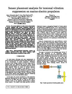
A torsional sensor for MEMS-based RMS voltage measurements
Recommend Documents
speed of 148 RPM with gear box ratios of 17/41 and 11/39, upper and lower bevel gears which is driven by an induction machine of 690V, 60HZ and 1200RPM.
True RMS Voltage Calculation with C. Xiao Xu. 11/14/12. Design Team 7.
Abstract. The ability to acquire fast and accurate True RMS values is extremely ...
AC-VOLTAGE REGULATORS M.Kaliamoorthy PSNACET. AC VOLTAGE
CONTROLLER CIRCUITS. (RMS VOLTAGE CONTROLLERS). AC voltage
controllers ...
and the possibility to reach a stability of the AC voltage measurement in a wide frequency range .... 2 Signals significant for the characterisation of the system.
Jul 10, 2008 - et al., 1985 ; Montal, 1990 ; Patten et al., 1999 ) evolution- ...... Kuo , A. , J.M. Gulbis , J.F. Antcliff , T. Rahman , E.D. Lowe , J. Zimmer ,.
May 11, 2006 - Jose S. Santos, Alicia Lundby, Cecilia Zazueta, and Mauricio Montal. Section of Neurobiology, Division of Biological Sciences, University of ...
E3S Web of Conferences 66, 01011 (2018) https://doi.org/10.1051/e3sconf/20186601011. AG 2018 â 4th International Conference on Applied Geophysics ...
a high-speed flywheel as temporary energy storage employed for braking and acceleration. The system is based on ... inst
Jan 15, 2013 - TipChip: a modular, MEMS-based platform for experimentation .... (h) Scanning electron micrograph of a trap entrance. Scale bar = 100 μm.
Rd disc. Motor shaft. Figure 1: Cable brake principle for torque measurements at a motor shaft. Fixed. Holder. Holder, displaced for loading. Sensor 2. Sensor 1.
Mar 6, 2007 - umbc.edu. Analytical Letters, 40: 715â727, 2007 ... Many analytical methods have been developed during the years for the measurement of ...
Measuring RMS Values of Voltage and Current. Voltage (Current) Measurements
. Effective Value. Standard classic measurements of voltage (current) values ...
Block diagram of the temperature meter. V ... By rotating the polarization beam splitter with the second 2/4 plate fixed, one can attain compensation of the flux.
In: Proc. NCSL, pp. 17-. 36, Albuquerque, USA, Aug. 1991. ... in Measurement, Geneva:International Organization for Standardization, 1995. [5] Hewlett-Packard ...
The Atomic Layer Thermopile (ALTP) is a novel fast-response sensor for transient heat flux measurements. The sensor's very fast frequency response allows for ...
of the system is appropriate for measurements of local scours. The apparatus was .... is 35 mm; water reduces sensing distances of approximately 50%. For the scour .... [17] Kothyari U.C., Garde R.J., Ranga Raju K.G. (1992), 'Tem- poral variation of
J. Nichols, C. Sandamali Weerasooriya, and J.W. Brill ..... measured frequency range and the values of the average relaxation time become very re la x a tio n tim.
the machine) and the dumping modules (its bucket) as shown in figure 3. Figure 1: Wheel Loader ... operation of the underground excavators, underground.
sults in a reduction of the effects of internal stiction and other ... improvement of the torque tracking performance. In [5] it has also been proved that the adequate ...
However, MacKinnon et al. (56) have shown that seg- ments S5, S6, and the pore loop of the voltage-dependent. Shaker K channel has close homology to the ...
Supporting Material. Interactions Between a Voltage Sensor and a Toxin via Multi-Scale Simulations. Chze Ling Wee, David Gavaghan, and Mark Sansom ...
Jan 22, 2014 ... Title Regression Modeling Strategies ... linear models. rms works with almost any
regression model, but it ..... uses units.default in Hmisc.
Aug 21, 2008 - arXiv:0808.2924v1 [cond-mat.other] 21 Aug 2008. Accepted by Nanotechnology 2008. Analyzing capacitance-voltage measurements of ...
[12] Ramatsetse, B.I., Matsebe, O., Mpofu, K. & Desai D.A. 2013. Conceptual design ... Reconfigurable manufacturing system for agile mass customisation ...
A torsional sensor for MEMS-based RMS voltage measurements
www.adv-radio-sci.net/6/31/2008/ ... RMS voltage-to-force conversion is an alternative method ... proportional to the square of its high frequency voltage is.
A torsional sensor for MEMS-based RMS voltage measurements 1 ¨ J. Dittmer1,2 , R. Judaschke2 , and S. Buttgenbach 1 Institute
for Microtechnology, Technische Universit¨at Braunschweig, Germany Bundesanstalt, Braunschweig, Germany
2 Physikalisch-Technische
Abstract. RF voltage measurement based on electrostatic RMS voltage-to-force conversion is an alternative method in comparison to the conventional thermal power dissipation method. It is based on a mechanical force induced by an RF voltage applied to a micro-mechanical system. For a theoretically adequate resolution and high precision measurements, the necessary geometrical dimensions of the sensor require the application of micro machining. In this contribution, the dependence between electrical and geometrical properties of different sensor designs is investigated. Based on these results, problems related to practical micro-machining and solutions with respect to possible sensor realizations are discussed. The evolution of different sensor generations is shown.
1
(Dittmer et al., 2007b) generation devices consecutively and analyze their performance from a fabrication process point of view. Similar devices have been developed by Bartek et al. (2000) in bulk- and Fernandez et al. (2003) in surface-micro machining technology. 2
Theory
Electrostatic voltage measurements are based on the principle of attractive forces induced by charge carriers of opposite polarity. Applying a voltage V to a capacitance C results in charge carriers Q on the electrodes. Taking account the virtual work analogy along with the stored energy in a capacitor W = 12 CV 2 , the work needed to separate the electrodes to a distance h is known to be W =FV h. Therefore the force FV acting on the electrodes is given by
Introduction
RF voltage measurement based on electrostatic RMS voltage-to-force conversion can be performed by a mechanically tunable capacitor having one elastically suspended electrode plate. By applying a voltage, a mechanical force proportional to the square of its high frequency voltage is generated between the plates and consequently, the plate moves to the equilibrium position between spring counterforce and electrostatic force. The position of the plate is measured using a second capacitor. Taking into account the necessary mechanical dimensions of a micro-machined sensor, several generations of devices have been developed. In this contribution we first discuss the theoretical basis for MEMS-based RF voltage measurement, with an emphasis on the design choices. We present an overview of first (Beissner et al., 2003), second (Dittmer et al., 2007a), and third Correspondence to: J. Dittmer ([email protected])
FV =
1C 2 V . 2h
(1)
If one of the capacitor plates is suspended elastically with a linear elasticity coefficient k, the necessary force Fk for a displacement x is Fk = kx.
(2)
Combining Eqs. (1) and (2) yields the equilibrium position for displacements x h0 to be x=
1 C 2 V . 2 kh0
(3)
Figure 1 illustrates this basic interaction. Concluding Eq. (3), it is obvious that a high capacitance with a small working distance along with a low stiffness of the suspension are necessary for a good device resolution. The conversion of a RMS voltage to a displacement depends on the inertia and damping of the system. Having an accelerated proof mass m and a velocity depended gas damping with a constant η leads to
Published by Copernicus Publications on behalf of the URSI Landesausschuss in der Bundesrepublik Deutschland e.V.
32
J. Dittmer et al.: A torsional sensor for MEMS-based RMS voltage measurements
Fig. 3. Interdigital, comb-like capacitance.
Fig. 1. Coupled spring-mass system with voltage excitation.
Fig. 4. Rotational design with opposing capacitances.
Fig. 2. Parallel plate capactitance.
a 2nd order dynamical system. The basic condition for measuring RF voltages is that the lowest measurement frequency ω is beyond any mechanical resonance frequency ωr of the system. Having a high proof mass is therefore critical for a good performance. An in-depth discussion for a rotational system is given e.g. by Sattler et al. (2002). 2.1
2.2
Parallel plate vs. interdigital sensors
In a first step, a choice has to be made which kind of capacitor to be used. State-of-the art micro machining provides two well-understood kinds of geometries: the first one, popular in silicon-on-insulator (SOI) based systems, uses interdigital or comb-like structures (Fig. 3). It is commonly used in accelerometers or gyroscopes and is well understood regarding manufacturing and calculating. From an electrical point of view, problems of the structure are unpredictable fringing fields not allowing a reliable direct calculation of the displacement resulting from an applied voltage. Therefore, a parallel-plate structure as shown in Fig. 2 has been chosen. Having a large capacitor area extensively suppresses the fringing fields except for the edges of the structure. Having big electrode areas, this effect can be neglected in a first order approximation. The equilibrium position for small displacements of a parallel plate capacitor with electrodes of an area A with an initial distance h0 can be found to be x=
1 ε0 A 2 U . 2 kh20
Adv. Radio Sci., 6, 31–34, 2008
Equation (4) shows that for a high sensitivity the initial distance h0 is the dominant quantity describing the the system. Parallel-plate capacitors in micro machining applications are used for example in RF switches or phase shifters fabricated in surface micro-machining technology. Thus, for RMS voltage measurements purposes, the low thickness of the actuated plate and therefore its light mass, and the low air damping coefficient due to the necessary openings and the resulting fringing fields make this technology unusable for the devices presented here. In bulk micro machining technology, a high mass and a closed flat area are achievable by combining multiple substrates.
(4)
Linear vs. rotational sensors
The second design choice for the sensing system, after selecting a parallel plate geometry, has to be made between a strictly linear parallel plate system, as shown in Fig. 3 and a rotational design, as illustrated in Fig. 4. Additionally a rotational design allows compensation measurements in comparison to a linear design. Unknown RF voltages can be directly balanced to known and precise DC voltages. As this is an important aspect for precision metrology applications, a rotational layout is chosen for the sensors discussed here. For large deflection angles, the electrical field is distored. However, as compensation measurements will primary be performed, where only the zero-deflection point is of interest, this disadvantage is not critical. 3
Devices
For the rotational design, different fabrication methods have been tested. Main part of each design is a bulk silicon torsional actuator. As mentioned before, bulk silicon is used due to its elastic behavior and the big achievable mass. It www.adv-radio-sci.net/6/31/2008/
J. Dittmer et al.: A torsional sensor for MEMS-based RMS voltage measurements
33
Fig. 5. Schematic of first generation device.
is also a readily available material in micro fabrication with good surface properties. Furthermore, several etchants are applicable, either for dry or wet processing. The actuator is finally embedded between two glass plates, providing the electrodes for readout and excitation connections and for environmental shielding. 3.1
First generation
The first generation devices (Beissner et al., 2003) have electrodes on both glass plates as shown in Fig. 5. The center actuator forms a common electric potential for all four electrodes. It is KOH wet etched, producing vertical side-walls by using the anisotropic crystallographic structure of silicon. The glass plates are anodically bonded to the actuator in a batch process, and afterwards the whole structure is diced. Is is a common problem during the bonding process that the actuator sticks to the glass wafers, producing non-functional devices. A second problem is the unreliable bond process due to the big open areas of the whole layout. Consecutively, this leads to water and particles in the cavities during the dicing process. Anodic bonding works best for closed surfaces. A third major problem are the bottom-up electrodes on the top glass wafer which makes the connections to surrounding electronics impractical. All these observations lead to the development of a second generation of devices. 3.2
Second generation
In the second device generation (Dittmer et al., 2007a), all electrodes are put on one side of the actuator without loss of functionality compared to the first generation. A cross section of the device is shown in Fig. 6. This solves the problem of wire-bonding of electrodes on two opposite sides. The glass cover serves only as protection sealing to prevent unwanted environmental influences. The second generation main actuator is dry-etched in an ICP enhanced process allowing more freedom in the geometrical design and thus betwww.adv-radio-sci.net/6/31/2008/
Fig. 6. Schematic of second generation device.
ter space exploitation. Experiments were made by using electroplated copper instead of gold electrodes with unsatisfactory results due to uneven, bowl-like surfaces. The actuator is anodically bonded to the bottom plate after dicing the parts. This improved the yield as a trade-off to a higher manufacturing overhead. As only four devices fit on one wafer the total work to yield ratio can still be improved. 3.3
Third generation
In the third device generation (Dittmer et al., 2007b), the structure is shrunk for a more efficient usage of the wafer area. The shrinking is mainly done by carefully reducing the bonding area and by replacing two big electrodes by smaller ones. The excitation electrodes still have the same size, as in the second generation. Thirteen 3rd generation devices can be placed on one wafer. To improve the isolation between the actuation and sensing electrodes, the common silicon electrode is replaced by multiple electrodes which are isolated from each other by using gold conductors on silicon oxide. These are connected to the base glass wafer by conductive glue. However, as this connection suffers from uneven glue distribution, unwanted interconnects, and short circuits occur frequently, reducing the yield. Typical geometrical dimensions of third generation devices are given in Table 1. Additional side electrodes are realized to detect skewed motion of the actuator. A cross section of the device is shown in Fig. 7 and an assembled device in Fig. 8. To improve the long-term reliability of the devices, bumpers have been added in the cavities of the sensing electrodes. These small bumpers are pyramidically shaped structures with a peak height below the gap height. They restrict the movement range of the actuator and hence prevent short-circuits between actuator and opposite electrodes as well es stiction of the actuator, which has been a major drawback of the previous device generation. Adv. Radio Sci., 6, 31–34, 2008
34
J. Dittmer et al.: A torsional sensor for MEMS-based RMS voltage measurements Table 1. Major geometrical sensor dimensions of a second generation device. Main electrode area
A
5 mm×5 mm
Side electrodes area
As
5 mm×2.5 mm
Gap distance
h0
10, 15, 20, 25 µm
Beam length
l
8 mm
Beam width
w
30, 40, 50, 60 µm
Lever
α1 L
1 mm
Base thickness
te
500 µm
Cover thickness
tc
500 µm
Body thickness
tb
370 µm
Fig. 7. Schematic of third generation device.
mized for batch fabrication allowing for a higher automation degree. The fabrication process is adapted to avoid any wet etching steps after etching the actuators. Acknowledgements. This research has been undertaken as a joined research project of the Institute of Microtechnology at the Technische Universit¨at Braunschweig and the High-Frequency Measuring Group of the Physikalisch-Technische Bundesanstalt, Braunschweig, Germany.
References
Fig. 8. Assembled third generation device.
Measurement results of third generation devices show the expected behavior for DC voltages. Due to the nonautomated assembly process, the absolute and relative measurement error is still too high. The RF behavior of the devices has also been investigated. A low pass behavior of the whole structure can be observed due to the high ohmic resistance and inductance of the long slender torsional beams. Also cross coupling between the excitation and measurement electrodes increase the capacitance measurement error, in the worst case making the results unusable.
4
Conclusions
In this contribution we discuss why an rotational parallel plate design is superior to a linear or interdigital design for RF voltage metrology. Different generations of designs are presented and their shortcomings are discussed. The fourth generation of devices is already under development, improving the electrical connection between base and body wafer by using press-on contacts. Also, the whole process is optiAdv. Radio Sci., 6, 31–34, 2008
Bartek, M., Xiao, Z., van Mullem, C., and Wolffenbuttel, R.: Bulkmicromachined electrostatic RMS-to-DC converter: Design and fabrication, in: Tech. digest MME 2000, 1–3 October, Uppsala, Sweden, p. A14, 2000. Beissner, S., Wogersien, A., Buttgenbach, S., Schrader, T., and Stumper, U.: Micromechanical device for the measurement of the RMS value of high-frequency voltages, Sensors, 2003, Proc. IEEE, 1, 631–635, 2003. Dittmer, J., Judaschke, R., and B¨uttgenbach, S.: Aufbau und Charakterisierung eines mikro-elektromechanischen Torsionssensors f¨ur die Hochfrequenzspannungsmessung, in: Mikrosystemtechnik Kongress 2007, Dresden, pp. 775–758, VDE Verlag GmbH, 2007a. Dittmer, J., Judaschke, R., and B¨uttgenbach, S.: A Miniaturized RMS Voltage Sensor Based on a Torsional Actuator in Bulk Silicon Technology, pp. 769–770, Micro- and Nano Engineering, Kopenhagen, 2007b. Fernandez, L. J., Visser, E., Sese, J., Wiegerink, R., Jansen, H., Flokstra, J., and Elwenspoek, M.: Radio frequency power sensor based on MEMS technology, Proc. IEEE Sensors, pp. 549–552, 2003. Sattler, R., Pl¨otz, F., Fattinger, G., and Wachutka, G.: Modeling of an electrostatic torsional actuator: demonstrated with an RF MEMS switch, Sensors and Actuators A, 97–98, 337–346, 2002.