International Journal of Advanced Information Science and Technology (IJAIST) vol.40, No.40, August 2015
ISSN: 2319:2682
Subthreshold Design of Second Generation Current Conveyor Mohd Ajmal Kafeel , Mohammad Zulqarnain
Mohd. Hasan, Muhmmad Shah Alam
Department of Electronics Engineering AMU, Aligarh, India
Professor/Department of Electronics Engineering AMU, Aligarh
[email protected] Abstract— Current mode circuits like current conveyors have attained significant importance especially in the field of current analog ICs design as compared to their voltage mode counterparts due to higher speed, lower power consumption and lesser chip area. This paper presents the design and optimization of ultra-low power second generation current conveyor (CCII) in the subthreshold region. Optimal sizing of transistors for different designs has been done at low supply voltages ranging from ±0.7V to ±0.25V. A design operating at supply voltage of ±0.25V and bias current of 20pA was found to be optimal. HSPICE simulations were performed to measure various performance parameters of CCII at the 32nm technology node.
Index terms –ultra-low power, subthreshold, current conveyor, current mirror, non-minimal length design. .
I. INTRODUCTION Ultra-low-power (ULP) design is important for biomedical systems. These systems should be small, consume minimum power and dissipate minimum heat. A fully implanted system with a battery that has a limited number of wireless recharges must operate under stringent low-power constraints such that constant surgery is not needed to change the battery in a patient. Thus, ULP operation will always be paramount in implantable biomedical systems [1]. ULP demands that the transistors should operate in the subthreshold regime where the supply voltage is lower than the threshold voltage of a MOS transistor. A. Subthreshold operation of a MOS transistor In subthreshold regime, the drain current in a MOSFET is given by (1) where is the technology dependent subthreshold current ⁄ is the thermal extrapolated for , voltage, is the aspect ratio and ‘n’ is the subthreshold factor [2]. The operation of MOS device in subthreshold region is necessary for ultra low power circuits [3]. A whole class of CMOS circuits has been developed for the weak inversion operation of MOS device [4]. The MOS device can be used to achieve higher gain in subthreshold region as is exponentially dependent upon . But the speed of
subthreshold circuits is severely limited because of large device sizes and low drain current [5]. It is possible to operate devices at quite low voltages in the range of 0.25-0.3V without sacrificing their functionality in subthreshold regime that reduces power consumption at the cost of reduced speed. There is a need of a basic building block that can be used to implement large number of different analog functions and that too in the subthreshold region. Second generation current conveyor (CCII) can be regarded as a real competitor for the operational amplifier (OPAMP). The classical OPAMP has suffered from constant gain band-width product problem and has low slew rate at its output. It has unreliable frequency response and remains unsatisfactory for high frequency applications. CCII, being a current mode device, has larger dynamic range, higher band-width, greater linearity, simpler circuitry, lower power consumption, and reduced chip area as compared to their voltage mode counterparts like Operational amplifiers. Due to its flexibility and versatility, CCII finds applications in realising impedance convertors, integrators, differentiators, filters etc. [6-9]. Few low voltage CCII structures have been reported so far operating at a supply voltage of 1V or less but they are unable to meet ultra-low power constraint on account of their complex structure [1012]. Current conveyor structures, characteristics and performance have been investigated in super-threshold region [13-14] but to the best of our knowledge its design, performance and characteristics have not yet been explored under subthreshold condition. Hence, this paper investigates, for the first time, the design and optimization of a CCII under subthreshold condition. The rest of the paper is organized as follows. A brief introduction of CCII is given in section 2. Section 3 and 4 deal with the design and performance analysis of various parameters of CCII for different designs. In section 5, variability analysis of optimal design is done using Monte Carlo analysis followed by the design of an instrumentation amplifier based on the designed CCII in section 6. Section 7 then concludes the paper.
1
International Journal of Advanced Information Science and Technology (IJAIST) vol.40, No.40, August 2015
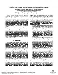
Figure 1 CCII block diagram
II. BASICS OF SECOND GENERATION CURRENT CONVEYOR The first generation current conveyor was introduced by Sedra and Smith in 1968. Later in 1970, they came up with a novel type of current conveyor known as second generation current conveyor [20-21]. Second generation current conveyor (CCII) is basically a versatile current mode (CM) device which conveys current with unity gain from the input port to the output port. With one high input impedance, one low input impedance and one high output impedance, it is a suitable element for both voltage-mode and current-mode circuits and can be used to perform many useful functions. The block diagram representation of CCII and its internal transistor implementation are shown in Figures 1 and 2 respectively. The characteristic equations of the dual output current conveyor can be represented as follows: IY=0 (2) VX=VY (3) IZ=±IX (4) where VX and VY are the voltages at ports X and Y, respectively. IX and IY are the currents entering ports X and Y. Moreover, IZ+ is the positive-type output current and IZ− is the negative type output current. Ideally, a current conveyor should satisfy the following conditions: 1) Infinite input impedance (RY) at port Y. 2) Zero input impedance (RX) at port X for current inputs. 3) Infinite output impedance (RZ) at port Z. 4) Unity current transfer gain between ports X and Z. 5) Unity voltage transfer gain between ports Y and X. 6) Infinite bandwidth.
ISSN: 2319:2682
configuration acts as a voltage follower. The output Z copies the current flowing through port X and is realized in the conventional manner using two complementary mirrors as current follower. The following section presents the design of a translinear loop based CCII in the subthreshold regime. The critical issue in designing translinear based CCII structure in the superthreshold region is the matching of NMOS and PMOS loop components in which µn and µp are process dependent parameters [14]. The situation becomes more critical in subthreshold region especially for submicron devices. Considering the various trade off conditions, different designs of translinear CCII structures are simulated using PTM 32nm level-54 model [16]. The performance evaluation of each design is carried out on the basis of various key characteristics of CCII namely current gain (α), voltage gain (β), current bandwidth, voltage bandwidth, resistances and their respective bandwidths at various ports of CCII. A. Design of classic translinear structure The design begins by transistor sizing on the basis of mobilities of NMOS and PMOS transistors. The adjusted aspect ratios of different transistors in [13, 23] are such that will keep all the transistors in the saturation region and they utilize 0.35 µm and 0.25 µm CMOS process parameters respectively. The optimal sizing of each transistor in this design of the current conveyor is done according [13, 23] using 32nm technology node. The supply voltage and bias current are adjusted such that all the transistors operate in the subthreshold region (Vgs < Vth). The aspect ratios of the transistors are listed in Table 1. The supply voltage is varied from ±0.7V to ±0.3V and the bias current is also changed for a particular supply voltage keeping all the transistors in the subthreshold region. All simulations are performed using HSPICE and performance parameters variations are plotted in Figures 4-10. Table 2 lists the performance parameters at ±0.3V supply voltage and at a bias current of 5nA and is compared with [13].
III. CCII STRUCTURES AND DESIGN CONSIDERATIONS Figure 2 uses a mixed translinear loop (transistors M1–M4) as the input of the CCII. Transistors M5, M7 and M10, M11 form two current mirrors that allow the mixed loop to be dc biased by the current. The input transistors present a high input impedance at port Y and a low impedance at port X. This
Figure 2 CMOS based circuit of CCII
84
International Journal of Advanced Information Science and Technology (IJAIST) vol.40, No.40, August 2015
Table 1. Transistors channel widths and lengths Transistor W/L M1-M2 1.28µm / 0.064µm M3-M4 M5-M9 M10-M13
ISSN: 2319:2682
lowering (DIBL) effect) and the bulk-source voltage (through the body effect) according to (7) where is the DIBL coefficient and is the body effect coefficient [24]. Since and source and body are at same potential, so , hence the above equation reduces to,
2.048µm / 0.064µm 0.768µm / 0.064µm 1.28µm / 0.064µm
Table 2. Performance parameters of CCII [13] This Design VDD
±1.5 V
±0.3 V
IB
50 µA
5 nA
α
1.02
1.0413
β
0.9515
0.9328
α-3dB (MHz)
393
5.38
(8) Where, Hence, current mismatch in subthreshold current mirror is exponentially dependent on drain to source voltage mismatch. The expressions for the current gain ( and voltage gain (β) is given as [25] = (9)
β-3dB (MHz)
503
6.14
Rx
1.44 kΩ
3.81 MΩ
RY
37.54 kΩ
124.06 MΩ
RZ
197.1 kΩ
185 MΩ
3dB RX (MHz)
-
18.7
3dB RY (MHz)
-
0.182
3dB RZ (MHz)
-
0.374
It can be observed from Table 2 that as the supply voltage and bias currents are reduced, there is a significant reduction in power dissipation as the transistors are moved into the subthreshold region at the cost of reduced bandwidth and higher port resistances. However, there is a considerable current mismatch in the current mirror as we move deep into the subthreshold region by reducing the bias current and supply voltage due to drain induced barrier (DIBL) lowering as explained below.
β=
=
(10)
It can be deduced from Figure 4 that for a particular supply voltage as the bias current increases, current gain tends towards unity. When the bias current increases, drain to source voltage mismatch of current mirrors reduces and hence from equation (8), current mismatch also reduces.Thus, current gain comes closer to unity.
B. Subthreshold current mirror By using equation 1, the ratio of drain currents of M1 and M2 can be written as follows:
(5) If both transistors have the same aspect ratio and Vds >4Vt ≈100mV, then (
) ≈1, and hence, the above equation
can be re-written as: (6) In equation 1, the threshold voltage also depends on the drain-source voltage (through the drain induced barrier
Figure 3. Basic Current Mirror circuit
85
International Journal of Advanced Information Science and Technology (IJAIST) vol.40, No.40, August 2015
Figure 5 shows the variation of the voltage gain with the bias current and the trends are just the reverse of Figure 4. For a constant supply voltage, if bias current increases then the deviation of the voltage gain from unity increases. As bias current increases, drain to source resistances rds reduces and hence from equation (10) voltage gain β deviates away from unity with β