tcd: the contamination delay (a.k.a. short-path delay) of the combi- national logic; ..... So the foot transistor for the dynamic NAND is eliminated. Note that ... fist half of the second cycle, a unexpected glitch, which can simulate a SET fault, takes ...
A Unified Online Fault Detection Scheme via Checking of Stability Violation Guihai Yan†‡ , Yinhe Han† , Xiaowei Li†∗ †
Key Laboratory of Computer System and Architecture, Institute of Computing Technology, Chinese Academy of Sciences, Beijing, P.R. China, 100190 ‡ Graduate University of Chinese Academy of Sciences, Beijing, P.R. China, 100039 {yan guihai, yinhes, lxw}@ict.ac.cn
Abstract In ultra-deep submicro technology, two of the paramount reliability concerns are soft errors and device aging. Although intensive studies have been done to face the two challenges, most take them separately so far, thereby failing to reach better performance-cost tradeoffs. To support a more efficient design tradeoff, we present a new fault model, Stability Violation, derived from analysis of signal behavior. Furthermore, we propose a unified fault detection scheme — Stability Violation based Fault Detection (SVFD), by which the soft errors (both Single Event Upset and Single Event Transient), aging delay, and delay faults can be uniformly handled. SVFD can greatly facilitate soft error-resistant and aging-aware designs. SVFD is validated by conducting a set of intensive Hspice simulations targeting 65nm CMOS technology. Experimental results show that SVFD has more robust capability for fault detection than previous schemes at comparable overhead in terms of area, power, and performance.
1. Introduction The development of semiconductor technology in the following decade will bring a broad set of reliability challenges at a dramatic fast pace [1]. Two of the paramount challenges are soft errors and agingdriven lifetime reliability. Many researchers focused on soft error modeling and mitigation within a wide design spectrum: device level, circuit level [2–4], microarchitecture level [5], and software level [6]. In addition, the industry and academic communities have done much work on understanding the semiconductor device reliability failure mechanisms and models, such as Electromigration [7], NBTI [8] [9] [10], TDDB, Hot Carrier Injection, Temperature cycling [11] etc. To mitigate aging effects, a promising approach is by aging-failure prediction[12][13]. Unlike soft errors, device aging is a gradual process. Before the devices totally breakdown and thereby loss their functionalities, they always tend to exhibit performance degradation, e.g. increased threshold voltage instability, soaring leakage power, worse heat characteristics etc. Most of these negative effects can result in the degradation of switch performance of the transistors[14], and eventually excessive path delay. In some words, most of the aging failures can be predicted by sensing the gradually increased aging delay. Agarwal et al. designed an aging sensor for this purpose. On the other hand, to alleviate the threats of soft errors, most approaches are redundancy-based, such as spatial redundancy by duplicating the flip-flops [2][15], or temporal redundancy by multiple-sampling [16]. However, those “redundancy” resources help little in mitigating aging effects, and even speed up the aging process due to the extra heat generated by those redundancy resources. This dilemma makes the goal of providing a not only aging-aware but also soft error-resistant scheme hard to achieve, unless a cumbersome combination of the previous aging-sensor and redundancy-based approaches is conducted. ∗ To whom correspondence should be addressed. This work was supported in part by the High-Tech Research and Development Program of China under grant No.(2007AA01Z109, 2008AA01Z147) and National Natural Science Foundation of China under grant No.(60806014, 60633060, 60831160526, 60776031), and by the National Basic Research Program of China under grant No.(2005CB321604, 2005CB321605).
978-3-9810801-5-5/DATE09 © 2009 EDAA
Rather than exploiting such a cumbersome combination, in this paper, we provide a unified mechanism to handle the two challenges. Based on the signal behavior analysis, we find that the soft errors and aging delay can converge into same signal behavior: Stability Violation. Even the conventional delay faults, which could result from transition hazard, crosstalk etc., can be brought into this behavior. Hence a unified fault model and detection mechanism can be exploited, thereby creating the chance of reaching a more optimum tradeoff between detection capability, design complexity, and implementation overhead. To our knowledge, this is the first work to handle the soft errors, aging delay, and delay faults under a unified fault detection mechanism. The main contributions of this paper are: 1) We propose a new fault model, called Stability Violation. We conclude that, at signal behavior level, the soft errors, aging delay, and delay faults can be uniformly modeled as Stability Violation. 2) Based on the new fault model, we propose an efficient online fault detection scheme—Stability Violation based Fault Detection (SVFD). SVFD can not only facilitate soft error-resistant design, but also aging-failure prediction. Besides that, SVFD can handle the conventional delay faults. The rest of this paper is organized as follows: Section 2 shows the related work and evaluates their limitations. Section 3 presents the SVFD mechanism. Section 4 addresses two major implementation concerns, which can greatly facilitate the circuit design presented in Section 5. Section 6 shows the experimental results. Section 7 discusses how to distinguish detection results, followed by the conclusion in Section 8.
2. Related Work Mitra et al. proposed a self-checking flip-flop design (SCFF)[2]. In their scheme, the scan portion of the scannable flip-flop is reused as redundancy of the flip-flop working in functional mode to detect SEU. Furthermore, through some clock manipulation—skewing the clock of the redundancy flip-flop [15], the modified flip-flop, referred as “LOWCOST”, can enable the SET detection capability. Although the “reuse” philosophy can reduce area overhead, it limit the applicability since not all circuit designs employ the redundancy-style flip-flop design, especially for some performance-critical pipelines where the sequential units are more timing-saving latches, rather than flip-flops. Moreover, this design can not be used for aging prediction. Agarwal et al. proposed a sensor design dedicated for aging failure prediction, called Aging Resistant Stability Checker (ARSC) [12]. The fundamental principle of aging prediction is delay detection since the aging process tends to induce performance degradation. Figure 1 shows the only difference between the aging delay detection and traditional delay fault detection: the former takes place in a safe timing interval called “Guard Band” [12], while the latter takes place in the interval after the effective clock edge called “Detection Slack”. The targeting “aging delay”, strictly speaking, is not a delay fault since it never translates into error. In contrast, a general delay fault can induce a error. ARSC inherently possesses little SET detection capability: the maximum detectable glitch width is TGB . In addition, it can not detect large SET, delay fault, and SEU. Recently, Nagpal et al. presented a Code Word State Preserving based flip-flop design (CWSPFF) [17] dedicated for SET protection.
Guard Band: TGB
Detection Slack: TDS
F li p -f lo p
ĂĂ
Si
Combinational So Logic
F li p -f lo p
clk
ĂĂ clk
Figure 1. Guard Band and Detection Slack
Figure 2. Generic Logic Circuit
The maximum detectable glitch width is min{tcd /2, (tpd −Δ)/2} (tcd and tpd are the contamination delay and propagation delay of a combinational logic, respectively). This limitation is more stringent than our approach in which the maximum detectable glitch width can easily excess tpd /2. Moreover, the CWSPFF can not be used to protect SEU and predict aging failures, and the area overhead is unattractive.
First, the Tvp , and Tsp for specified signals need to be established respectively. Figure 2 models a general logic circuit. The input signal Si comes from the upstream flip-flop, and the output So is captured by the downstream flip-flop. The both flip-flops are synchronized by the same clock clk with cycle period of T . Several timing parameters are denoted as: tpd : the propagation delay of the combinational logic; tcd : the contamination delay (a.k.a. short-path delay) of the combinational logic; tcq : the flip-flop’s clock-to-q time. The Si is updated at every effective clock transition, and is held on for the whole time period, which means there is almost no variable period exist. Thus the stable value, the variable period, and the stable period of Si in the nth clock cycle ((n − 1)T, nT ) can be expressed as:
3. SVFD: Stability Violation based Fault Detection First, we specify the target fault types. Then, we present the unified Stability Violation model and the SVFD mechanism. 3.1
Target Fault Types For an on-line fault detection mechanism, three classes of faults are particularly significant: Soft Error: Single Event Upset (SEU) and Single Event Transient (SET) [18]. If some high energy radioactive particles induce a storage cell to be flipped, this unintentional bit-flip is called SEU. If the particles cause a node of combinational logics to collect enough charge, a transient current pulse could be generated. This pulse can transform into a voltage pulse and propagate along logic paths [19]. This type of soft error is called SET. A soft error might not be captured by flip-flops due to three masking effects [19]: Logic Masking, Electrical Masking, and Latching-window Masking. Aging Delay: the aging effects, such as NBTI, can cause aging delay which can be used for aging-failure prediction[12]. Usually, the aging delay increasing is a gradual process over time, but the abrupt delay increasing is possible when the devices suffer from breakdowns induced by mechanical stresses. This type of “abrupt” aging delay will not be covered in this paper. Delay Fault: This type of faults refers to the conventional delay faults [20] which is caused by device defect, signal crosstalk, etc. We just cover the delay fault whose size is less than the width of the Detection Slack. 3.2
Modeling Faulty Signals Mathematically, a signal S can be expressed as a function of time t, that is S = f (t). Given the time interval of (ti , tt ), in which S can get into a stable state before tt . The interval (ti , tt ) is divided into S variable period, denoted as Tvp = (ti , ts ), and stable period, denoted S as Tsp = (ts , tt ), where ts is the complete time of the last transition of S. The initial value and the terminal value of the signal are denoted as FiS = f (ti ), and FtS = f (tt ), respectively. According to the above definition, we define a faulty signal, Sf , that commits at least one of the three violations: S 1) Initial Value Violation (IVV): The obtained value of Fi f at time ti differs with f (ti ). S 2) Terminal Value Violation (TVV): The obtained value of Ft f at time tt differs with f (tt ). 3) Stability Violation (SV): One or multiple transitions happen in the stable period. There are some correlations among the three types of Violations. For example, the TVV of a signal could cause the IVV of another signal; A SV of a signal can cause the TVV of the signal itself. The above violation behaviors, strictly speaking, can not precisely capture all details of signal mismatch between a fault-free signal and its faulty counterpart. Practically, however, the above violation rules are robust enough to guide high efficient on-line fault detection. In fact, given the target fault types (Section 2.1), only the Stability Violation of a signal is needed to be verified. Rather than mathematically describing the application of the violation based fault model, the following will explain how to use this model in a practical way.
Si Tvp = ((n − 1)T, (n − 1)T + tcq )
(1)
Si Tsp
(2)
= ((n − 1)T + tcq , nT )
Unlike Si , So has a wider variable period. The So ’s stable value, variable period, and stable period are expressed as: So = ((n − 1)T + tcq + tcd , (n − 1)T + tcq + tpd ) Tvp
(3)
So Tsp
(4)
= ((n − 1)T + tcq + tpd , nT + tcq + tcd )
Figure 3 illustrates the above time period in the nth cycle, where t1 = (n − 1)T + tcq + tcd , t2 = (n − 1)T + tcq + tpd . Variable Period
Stable Period
Si So
Time (n-1)T
t1
t2
nT
Figure 3. Variable Period VS. Stable Period
Then, we can explain how a target fault (delay fault, SEU, and SET) results in some of the above violations, and how these IVV, and TVV converge to SV. 1) Suppose that a delay fault occurs, the delayed So will cause SV in Detection Slack (TDS ) during which the So should keep stable. Equivalently, the delay fault will result in So ’s TVV since at the end of the cycle, So can not reach the expected value. This TVV then causes the IVV of the signal in the next stage of logic. So, SV, TVV, and IVV are equivalent to each other for the delay fault. 2) Suppose that an aging delay occurs, the delayed So will cause SV in Guard Band (TGB ). Unlike the delay fault, the aging delay will not cause TVV and IVV. So, an aging delay just represents as SV. 3) Suppose that an unmasked SEU takes place in the upstream flipflop. Clearly, the Si ’s SV is committed because, after a short clockto-q time, Si is supposed to keep stable during the whole cycle period. this Si ’s SV could potentially cause the downstream flip-flop to capture faulty data, and thereby results in So ’s TVV, then IVV of input signals in the next stage logic. So, the SEU will represents as SV, and possible IVV and TVV. 4) Suppose that an unmasked SET happens in the combinational logic. If the duration of the SET is less than TDS + TGB , the SET fault behavior is similar with the delay fault: the unexpected signal transitions within the So ’s stable period. Therefore, the analysis result for the delay faults is held for SET faults. That is SV, TVV, and IVV are equivalently to each other for the SET.
A valid execution of a logic (shown in Figure 2) implies that the flip-flops capture “right data at right time”. Generally, the right time is guaranteed by a set of optimized system clocks. In this study, we mainly concern about the integrity of the data at right time. 4.1
Manipulate Precharge Period A general checker design is based on the dynamic circuit style. The first concern is how to schedule the precharge period because the traditional cycle-begin precharge or cycle-end precharge styles are unapplicable in our detection mechanism. As Section 3.2 explained, during the Guard Band and Detection Slack, the checker should be on duty, rather than stay in precharge state. For So the precharge can be scheduled for its variable period. However, the same schedule strategy is unallowable for Si because there is almost no any variable period can be employed for precharge. If we “brutally” borrow some time from Si ’s stable period for precharging the checker, the fault coverage is hard to be guaranteed. To address this problem, we find if the precharge stage is scheduled according to some specific timing requirements, the fault coverage will not be sacrificed. The timing manipulation is based on the key observation, called as Propagation of Stability Violation. Suppose that an unmasked SEU occurs in the upstream flip-flops at time t in the nth cycle, then the effects of the Stability Violation of Si will be propagated to So within the time period of (t + tcd , t + tpd ). If the effects of Si ’s stability violation can propagate into So ’s stable period, that is
Comb. Logic
So(k-1)
(K-1)th stage
Comb. Logic ĂĂ
Sik
Kth stage
clk
Figure 4. XOR Protection
Then, we can derive the start point of the available precharge time is nT − tcd − TGB . Additionally, to avoid Detection Slack violation, the actual start point of the precharge stage should be max{(n − 1)T + TDS , nT − tcd − TGB }
(7)
If we schedule precharge stage within this period of
the fault coverage will not be sacrificed. The available precharge duration τ can be expressed as τ =
TDS + TGB + tcd − tpd T − tpd
(6)
Clearly, not all unmasked SEUs taking place in the upstream flipflop can translate into the So ’s SV; e.g. if a Si ’s SV happened during the ((n − 1)T, t1 ) (Figure 3), then it could not be detected by So ’s checker because Eq.(5) can not be held any more. To cover this period, one way is setting another stability checker for Si , at the expense of almost doubled area, power and complexity. In contrast, we employ a simple but far more efficient way to cover this period, referred as XOR Protection, as Figure 4 shows. The effec(K−1) tiveness of this scheme based on the key observation: the So is K consistent with the Si within the period of ((n − 1)T, t1 ); therefore one XOR gate is capable of capturing any SiK stability violation during this time. Clearly, the overhead imposed by a XOR gate is far more efficient than that imposed by another stability checker or other traditional redundancy flip-flop based schemes [2]. How to efficiently handle the output of XOR will be present in Section 5.
if tcd < T − TGB − TDS , otherwise.
To sustain normal operations, there is a minimum precharge duration τ0 , which is determined by the intrinsic RC constant. Clearly, τ > τ0 needs to be meet. 4.2
Eliminate SEU detection “Blind Zone” Considering the propagation delay of a SEU, we can claim that the SEU must be benign if (8) t > nT − tcd . For Si protection, besides the XOR protection period, the Propagation Detectable period, and the benign period, there might be the fourth region that has not be covered so far. Figure 5 shows that the whole Stable Period of Si could be divided into four or three zones depending on different timing parameters. nT-tcd nT-TGB
XOR Protection Time
(n-1)T
nT
nT-tcd-TGB nT-tpd+TDS (a) nT-tcd
(5)
The SEU induced Si ’s SV will be represented as So ’s SV since the So should keep stable during the Guard Band and Detection Slack. Thus, the checker for detecting So ’s SV now can naturally handle a part of Si ’s SV within the particular time interval, referred as Propagation Detectable Period (PDP). From (5), we can obtain the PDP as nT − TGB − tcd < t < nT + TDS − tpd .
ĂĂ
(max{(n − 1)T + TDS , nT − tcd − TGB }, nT + TDS − tpd ),
4. Implementation of SVFD
(t + tcd , t + tpd ) ⊆ (nT − TGB , nT + TDS );
Sik Stability Violation
FFs
From the above analysis we can conclude that, at the signal behavior-level, the target faults either induce equivalent SV, IVV, and TVV (for delay fault and SET), or only represent as SV (for aging delay), or SV and possible equivalent IVV and TVV (for SEU). In other words, the target faults can be uniformly modeled as SV. The implication is that we can employ a unified stability checker to handle the detection for all the target faults. This unification can support more efficient implementation of an online fault detection scheme than traditional redundancy-based approaches [2][3]. More attractively, the capability for aging failure prediction [12][13] can be readily exploited in place with the same scheme. The following section presets the implementation of SVFD mechanism. In particular, two major practical design considerations are covered, which can greatly facilitate the circuit design (in Section 5).
Precharge Stability Protection
nT-TGB Safe(Benign) Time
(n-1)T
nT-tcd-TGB
(b)
nT-tpd+TDS
nT
Figure 5. Variety of Timing Period
Figure 5(a) shows if nT −tpd +TDS < nT −tcd , then a SEU taking place in the zone of (nT −tpd +TDS , nT −tcd ) may not propagate into a detectable period, thereby resulting in detection “Blind Zone”. Unlike the XOR protection period, this trouble can not be eliminated unless another dedicated stability checker is set for Si , at considerable expense of implementation overhead. However, we propose a new approaches: Contamination Delay Optimization, by which the “Blind Zone” can be eliminated by some timing manipulation. Contamination Delay Optimization: Clearly, the “Blind Zone” can be naturally eliminated if nT − tcd < nT − tpd + TDS
(9)
is satisfied, as Figure 5(b) shows. The SEU taking place in (nT − tcd − TGB , nT − tpd + TDS ) is either propagated into a Stability Violation detectable zone of So , or have nothing bad effect due to being benign period. From (9), we get tcd > tpd − TDS
(10)
CLKS Stability Checker
nT-tcd
Aging delay Detected
Fault Detection Unit
CLKG
Time
Soft error/Delay fault Detected
Precharge (n-1)T
nT Max{nT-tcd-TGB, (n-1)T+TDS} nT-tpd+TDS
SiK
CLK
Kth stage
SoK
Flip-flop
So(K-1)
Flip-flop
ĂĂ
Combinational Logic
CLK
Si(K+1)
XOR Protection
nT-TGB
Propagation Detectable
ĂĂ CLKS
CLK
Benign(SEU)
CLKG
Figure 6. Top View of SVFD Scheme
In addition, the XOR protection zone should meet nT − tcd − TGB < (n − 1)T + tcd + tcq 1 ⇒ tcd > (T − TGB − tcq ) 2
Figure 7. Precharge Clock and XOR Gating Clock Timing
(11)
From (10), and (11), tcd should meet the requirement: tcd > max{tpd − TDS ,
1 (T − TGB − tcq )} 2
(12)
Generally, (12) requires the contamination delay of the combinational logic reaches up to about a half cycle period. This same requirement is needed to be satisfied in some previous studies [15] to address “short path effects” [21]. Actually, It is consistent with the goal of variety timing optimization strategies [22][23], and therefore not a substantial limitation. A byproduct coming with the Contamination Delay Optimization is that the terminal time of precharge period can be extended from (nT − tpd + TDS ) to (nT − TGB ) since the checker does not need to be on duty from time (nT − tpd + TDS ) to (nT − TGB ) any more. Combined with (7), we can derive the available precharge period after eliminating the “Blind Zone” as (max{(n − 1)T + TDS , nT − tcd − TGB }, (nT − TGB )). (13) Actually, (13) shows that the available τ is easy to excess τ0 . Experiment results indicate that for 65nm CMOS, 1GHz, τ0 is merely 40ps, while τ is at least at the magnitude of hundreds of picoseconds. To sum up, we can use only one stability checker, with the assistant XOR protection, for soft errors, aging delay, and delay faults detection. Figure 6 shows the top view of the whole fault detection scheme. Note that the XOR output needs to be gated beyond the XOR protection period. Figure 7 shows the overall timing relations. The CLKS is used to precharge-evaluation control, and the CLKG is the gating clock for XOR output.
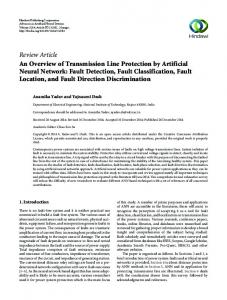
5. Circuit Design Figure 8 shows the transistor level design of SVFD scheme which consists of two key components: a stability checker(Figure 8(b)) and a output compressor (Figure 8(c)). The basis stability checker can be derived from a sensing circuit for on-line delay fault detection [20], in which the signal integrity is verified by a pair of consistent charge/discharge nodes, a delay fault will trigger one of the nodes to be discharged/chargeed and thereby causes states inconsistent between them. The same fundamental detection principle is employed to design a sensor dedicated for aging prediction, referred as Aging Resistant Stability Checker (ARSC) [12]. Based on the same principle, we design a new stability checker. Compared with ARSC, the checker has several new features which can improve the robustness and reduce the overhead. The following explains 1) how does the circuit work, and then 2) presents the new features. During precharge period, both nodes S1 and S2 in stability checker are charged up to HIGH. Then, the circuit starts evaluation, one of the two nodes is pulled down, while the other one floats at HIGH because
the gate signal of M3 is always complemented with that of M4. A keeper can help the floated node stick to HIGH. The node S1 and S2 are always exclusive during fault-free time, which will make the node S4 stick to HIGH because the high-impedance path between S4 and GND always exist. When a Stability Violation is committed by Si (out of the XOR protection period) or So , the violation will trigger the discharge of the node that has charged up to HIGH. Eventually both nodes are discharged, and thereby the node S4 is pull down to LOW. Then, the node X in output compressor will be discharged, which flags a fault being detected. The compressed result X needs to be latched twice: CLK-latched for indicating aging delay and CLKG-latched for indicating soft error or delay fault (Figure 8(d)). The reason will be explained in Section 7. There are two new features in the detection unit. 1) The NOR logic for combining the states of S1 and S2 is realized with a dynamic logic (M6, M7, and M8), which can improve the robustness of the checker and reduce the area overhead and switch power dissipation. Unlike the stability checker in ARSC [12], where the checker output, a static NOR gate, is directly driven by a floated HIGH node during fault-free time, our checker’s output is generated by a dynamic NAND gate. This change is based on the key observations: during precharge, both the node S1 and S2 are pulled up to HIGH, consequently, both M7 and M8 are turned off; thereby no short path exist when precharge. So the foot transistor for the dynamic NAND is eliminated. Note that due to the precharge RC delay of S1 and S2, the M6’s precharge clock should be delayed by a precharge delay constant, though this delay is not necessary during the dominated fault-free time. 2) The outputs are compressed for reducing the number of output latches. Since such fine-grained detection results, which are for every signal, are not necessary for the most recovery or aging-aware designs. This relaxation creates the chance of compressing the detection results for reducing area overhead. We use a wide dynamic NOR to realize the compressor, in which the M11 and M12 serve as a level restorer for node X. In addition, this detection unit can be easily disabled by pulling up the CLKS to HIGH. The PMOS transistor’s aging process induced by NBTI effects is greatly slow down in disable mode. Unlink ARSC, where the Guard Band is confined by a clock and its delayed counterpart [12], SVFD unit provide Guard Band by the CLK and CLKS. So the clock skew needs to be controlled well and thus incur potential complexity overhead. This issue is beyond the scope of this paper.
6. Experiments The experiments consist of two parts. The first is dedicated for detailed timing verification; the second presents the overhead in terms of area, power dissipation, and performance. The results are obtained by using the Hspice targeting the 65nm Predictive Technology Model [24]. Table 1 shows the related experiment parameters. VDD 1.25V
Table 1. Experiment Parameters (65nm CMOS) Vth T TGB TDS tcq tpd tcd 0.42V 1 ns 0.1ns 0.5ns 10ps 0.85ns 0.45ns
Using (13), we derive the precharge clock’s duty cycle is: (0.5ns, 0.9ns). The duty cycle of the signal gating clock, CLKG, is: (0.5ns, 1ns) (Figure 7).
STABILITY CHECKER XOR Protection
B1
CLKG
Co_b Co
VDD
VDD
M1
M2
CLKS
S1
Si
K-1
Flip-flop Q D
Cin
Comb.
Si
So
S4
S3
(a) Q
I D
A1
X
I
CLKS
Y
I
GND
CLKG
(c) I
(d)
Q
X
I
I
I
I
GND
(e) Latch
CLK Soft error/Delay fault Detected Latch
GND
I
I
Aging Delay Detected
GND
D
X
I
Bn
M10
(b)
VDD
Y
An
M12
S5
Co_b
Latch
Y
I
I
B1
M8
GND
Co
M11 X
M7
M5
CLK
OUTPUT LATCH
VDD
M9
M4
K
COMPRESSOR VDD
M6
S2
M3
K
CLKS VDD
(f) Flip-flop
I
Figure 8. SVFD Implementation Guard Band � CLK CLKS�
Detection Slack�
Normal Transions� Fault Transions�
XOR So�
SEU fault �
Aging delay �
Voltage �
S1 S2�
A1 B1� Fault detected�
X�
Fault detected�
Fault detected�
Time�
Figure 9. Hspice Simulated Signal State Transitions
SVFD Unit �
Instant Power�
Figure 9 shows the detail timing of a SVFD unit in 4 cycles. The topmost shows the system clock CLK, the precharge-evaluation clock CLKS. The second shows the monitored signals: XOR protection output and So . The third illustrates the state transitions of the two most important node S1 and S2. The forth shows the signals A1, the output of the stability checker, and B1, the gated output of XOR protection unit. Both are feeded to the compressor. The bottommost shows the detection result generated by the compressor. During the first cycle, So presents some normal transitions. In the fist half of the second cycle, a unexpected glitch, which can simulate a SET fault, takes place; then in the guard band of the second cycle, a aging delay is simulated. The third cycle is fault-free. In the fourth cycle, a SEU fault is simulated by XOR signal. From the bottom figure, we can see that all the Stability Violation shown in the second waveform are successfully detected. We zoom in the figure to extract some useful timing information (the zoomed figures are omitted due to space limitation): 1)the critical precharge time τ0 is about 40ps, while the available precharge time is 400ps, far larger than that. So the precharge time will not be a limitation when we manipulate the related timings (Section 4.1). 2)The detection delay is just about 45ps is just about 3 FO4 delay in 65nm technology. 3)The maximum undetectable glitch width is about 18ps, which is even less than most soft error induce glitch width in 65nm technology, so the robustness of SET detection should not be in question. Table 2 shows the tradeoffs comparison among the SEFF [2], LOWCOST [15], ARSC [12], CSWPFF [17], and SVFD. we use the number of transistors as the area overhead metric, as many circuit-level studies take. Area: To conduct comparisons between variety schemes, a baseline latch and flip-flop design needs to be determined. Figure 8(e) and (f) show the adopted baseline design. The similar latch design is used by Intel as a standard datapath latch [25]. The flip-flops is used in PowerPC603 processor [26]. In addition, a XOR gate consumes at least 12 transistors when computing the number of transistors. For fairness,
Functional Flip-flop�
0�
1n�
2n�
3n�
4n�
Time�
Figure 10. Instant Power Comparison Between a Standard Flip-Flop and SVFD Unit
only the checker and its input generating logics are considered; the subcomponents that can be shared among checkers (i.e. output compressor, and output latches) are not taken account though such amortization will make the area overhead of SVFD more attractive. Power: Another concern is about power overhead. We compare our SVFD unit’s instant power against that of a standard flip-flop(as shown in Figure 8(e)) with the same input signal (Figure 9(b)) and frequency. Figure 10 shows that our SVFD’s power consumption PSV F D is comparable with a standard flip-flop’s power consumption PF F . We use Hspice to integrate the waveform over time and then get the average power relation: PSV F Davg ≈ 0.96 PF F avg . SEFF’s power is doubled, as [2] shows, is because the redundancy flip-flop is enabled. Similar modification is conducted in LOWCOST; moreover, a extra lath is employed. So the power of LOWCOST must be larger than that of SEFF. Note that our checker seems more power-hungry than ARSC. That is because the power overhead metric in [12] is different with ours. In ARSC, the power overhead is calculated as the whole logic (include both the flip-flop and combinational logic) power increase. Because the combinational logic’s power is relatively constant, so the actual sensor power consumption compared with flip-flops should be much higher.
Table 2. Comparing Tradeoffs with other schemes SEFF[2] 14 2 0 1 Limited�
LOWCOST[15] 36 >2 N/A 2 Limited
ARSC[12] 24 >1.1�