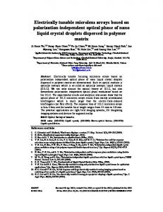
INSTITUTE OF PHYSICS PUBLISHING
NANOTECHNOLOGY
Nanotechnology 17 (2006) 3786–3790
doi:10.1088/0957-4484/17/15/029
A universal approach to electrically connecting nanowire arrays using nanoparticles—application to a novel gas sensor architecture Prahalad M Parthangal1,2 , Richard E Cavicchi2 and Michael R Zachariah1,2,3 1
Departments of Mechanical Engineering and Chemistry, University of Maryland, College Park, MD 20742, USA 2 Chemical Science and Technology Laboratory, National Institute of Standards and Technology, Gaithersburg, MD 20899, USA E-mail:
[email protected]
Received 1 May 2006, accepted for publication 1 June 2006 Published 6 July 2006 Online at stacks.iop.org/Nano/17/3786 Abstract We report on a novel, in situ approach toward connecting and electrically contacting vertically aligned nanowire arrays using conductive nanoparticles. The utility of the approach is demonstrated by development of a gas sensing device employing this nano-architecture. Well-aligned, single-crystalline zinc oxide nanowires were grown through a direct thermal evaporation process at 550 ◦ C on gold catalyst layers. Electrical contact to the top of the nanowire array was established by creating a contiguous nanoparticle film through electrostatic attachment of conductive gold nanoparticles exclusively onto the tips of nanowires. A gas sensing device was constructed using such an arrangement and the nanowire assembly was found to be sensitive to both reducing (methanol) and oxidizing (nitrous oxides) gases. This assembly approach is amenable to any nanowire array for which a top contact electrode is needed. (Some figures in this article are in colour only in the electronic version)
1. Introduction Despite significant advancements in nanowire growth techniques and device descriptions, establishment of electrical contacts to nanowire assemblies through non-destructive methods has not yet been successfully realized. The commonly employed method involves physically removing nanowires from the sample, dispersing them in solution, and transferring them onto another surface containing probe pads, and depositing contact electrodes onto individual nanowires through some form of lithography. Such a series of steps are not only destructive, but also expensive and tedious. Another method described in the literature involves burying the nanowire array in an insulating matrix such as spin-on glass or polystyrene, followed 3 Author to whom any correspondence should be addressed.
0957-4484/06/153786+05$30.00
by plasma etching to expose the nanowire tips [1, 2]. However, this approach prevents access to the surface of the nanowires, which would be necessary for applications like gas sensing. In this paper, we describe a simple method for growing electrodes in situ in contact with the top of a vertically aligned nanowire assembly by selectively attaching gold nanoparticles to the tips of nanowires and forming a continuous film. The electric field enhancements around the sharp tips of nanowires as well as their high aspect ratios are exploited in this procedure, which is generic to a wide range of nanomaterials and nanostructures. The result is a device, which is an ensemble of single nanowire devices connected in parallel. For sensor applications there may be signal to noise advantages in such an arrangement compared to single nanowire devices. Previous nanowire-based sensors have involved disordered nanowire networks, where electrical contact is determined
© 2006 IOP Publishing Ltd Printed in the UK
3786
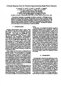
A universal approach to electrically connecting nanowire arrays using nanoparticles Cr/Au catalyst pads
ZnO NW on Au
(b)
SiO2 substrates
Unexposed Au layers
(a)
ZnO NW on SiO2
Figure 1. (a), (b) represent substrate surfaces before and after nanowire growth respectively. Clean SiO2 wafers were placed on top of the substrate before nanowire growth to enable electrical contact to the bottom of the nanowires grown on each individual catalyst pad.
primarily by the contacts between individual nanowires [3–6]. In contrast, this new device’s properties reflect the electrical transport along isolated nanowires. Our approach may also be suitable for electrically driven optical devices based on nanowires. We chose to grow and study a nanowire assembly of zinc oxide (ZnO), owing its great potential in the development of new electronic and photonic devices. ZnO is a widebandgap semiconductor ( E g = 3.37 eV) with a wurtzite crystal structure that has been grown into several morphologies including nanowires [3, 7], nanocombs [8], nanobelts [9], nanorings and nanoribbons [10] etc through both gas-phase and solution-phase syntheses [11]. One-dimensional ZnO nanowires have been observed to act as gas sensors [3], room temperature ultraviolet (UV) lasing cavities [12], UV/visible photodetectors [13] and field effect transistors [14]. Synthesis of well-aligned nanowire arrays of ZnO is of prime importance for the realization of nanoelectronic devices such as light emitting diodes (LEDs) and laser diodes. Several groups have synthesized ZnO nanowires by simple thermal evaporation of commercial Zn and ZnO powders [15, 16]. Metal–organic chemical vapour deposition (MOCVD) of ZnO nanorods has also been described using precursors like diethyl zinc and zinc acetylacetonate hydrate [17, 18]. In this work, we grew nanowire arrays of ZnO on gold (Au) catalyst layers deposited on silicon dioxide (SiO2 ) substrates, through direct thermal evaporation of Zn powder within a tube furnace maintained at 550 ◦ C. The nanowires were found to be well aligned and vertically oriented, with an average diameter of 60–75 nm and had faceted, hexagonal heads, with a growth direction along the c-axis.
2. Experimental section
a quartz tube placed within a horizontal tube furnace, the substrates being held 5 cm downstream of the Zn powder. The tube was then evacuated using a rotary mechanical vacuum pump, and this was followed by the introduction of 150 sccm (standard cubic centimetres per minute) nitrogen (N2 ) and 10 sccm oxygen (O2 ) and brought back up to atmospheric pressure. The nanowires were grown at 550 ◦ C for about 2 h and the substrates were then cooled down to room temperature. A schematic diagram of the substrate surface before and after nanowire growth is shown in figure 1. 2.2. Nanoparticle generation and deposition Au nanoparticles were generated through an aerosol spraypyrolysis method. A 0.03 M (mol l−1 ) aqueous solution of hydrogen tetrachloroaurate (HAuCl4 ; Sigma Aldrich Inc. (see footnote 4)) was sprayed into droplets with an atomizer, using a carrier gas flow of 2 slpm (standard litres per minute) N2 . The flow containing the droplets was passed through silica gel dehumidifiers, and then into a tube furnace maintained at 600 ◦ C, to thermally crack the precursor and form Au particles. The particles were then positively charged with a homebuilt unipolar charger and introduced into an electrostatic precipitator containing the substrate with the grown nanowire arrays of ZnO. A high negative electric field of −10 kV cm−1 was applied to drive the particle deposition. 2.3. Nanowire characterization and gas sensing measurements The morphology of the substrates was imaged using a Hitachi S-4000 scanning electron microscope (SEM (see footnote 4)). Wide-angle x-ray diffraction (XRD) patterns were recorded on a Siemens D-500 diffractometer using Cu Kα radiation, while transmission electron microscopy (TEM) and selected area electron diffraction were performed using a Zeiss CM 10 microscope (see footnote 4). For gas sensing measurements, the sample was glued onto a large square package containing pin contacts for electrical connections using a high temperature adhesive paste (Ceramabond 503; Aremco Products Inc., NY (see footnote 4)). Wire bonds were attached to all four gold pads for resistance measurements. Controlled mass flow rates of test gases and zero-grade dry air were delivered through a computer-automated delivery system, to the sample that was placed on a temperature-programmable hotplate. Fixed temperature responses of the nanowire array (at 325 ◦ C) to various concentrations (10–50 ppm—parts per million by volume or µl l−1 ) of methanol (CH3 OH) and nitrous oxide (NOx ) were measured and analysed.
2.1. Growth of ZnO nanowire arrays Silicon dioxide wafers (1 cm2 ) were ultrasonically cleaned in acetone and four square pads of 15 nm of chromium (Cr) followed by 150 nm of gold (Au) were deposited (Cr was deposited to ensure better adhesion of Au to the substrate). The substrates were then placed in an alumina boat containing commercial Zn powder (Aldrich, 99.5%4 ), and loaded into 4 The identification of any commercial product or trade name does not imply endorsement or recommendation by the National Institute of Standards and Technology.
3. Results and discussion 3.1. Morphology and crystallography of ZnO nanowire arrays SEM images of the ZnO nanowires are presented in figure 2. The nanowires grown on the Au catalyst layer are well aligned along the vertical direction with widths between 60 and 80 nm, and lengths between 5 and 10 µm, while the nanowires on the adjacent SiO2 portion are more randomly oriented. Figure 3(a) represents a typical XRD pattern obtained from the 3787
P M Parthangal et al
Au
(a)
SiO2
(b)
Figure 2. (a) SEM image of ZnO nanowires grown on Au and SiO2 (left and right portions) clearly indicate alignment of nanowires on Au and lack of alignment on SiO2 . (b) A closer look at the well-aligned nanowire array of ZnO on Au. Scale bars for (a) and (b) are 10 µm and 3.75 µm respectively.
7000
Intensity (a.u.)
6000
nanowires. Growth on SiO2 generally follows a non-catalytic vapour–solid (VS) mechanism [20–22], in which zinc and zinc suboxides condense on the SiO2 surface to form droplets which act as nuclei for ZnO nanowire growth.
(002)
(a)
5000 4000
3.2. Nanoparticle film contact description and I –V characteristics of ZnO nanowire array
3000 2000 1000 0 30
40
50
2Θ Θ
60
70
80
(b)
Figure 3. (a) XRD pattern of ZnO nanowire array grown on Au. (b) Low resolution TEM image of ZnO nanowires (scale bar = 500 nm). Inset depicts electron diffraction patterns arising from a nanowire, indicating that the wires are single crystalline.
nanowires, where the sharp peak at a 2-theta value of 34.42◦ corresponds to the (0 0 2) plane of the hexagonal ZnO crystal. TEM and electron diffraction analysis of individual nanowires revealed that the nanowires are single crystalline, with a growth direction along the c-axis of ZnO, shown in figure 3(b). The growth mechanism for the nanowires on Au generally follows a vapour–liquid–solid (VLS) mechanism [7, 19, 20], wherein Zn vapour is transported and reacted with the Au catalyst, forming alloy droplets which provide nucleation sites for ZnO vapours to condense and grow into well-crystallized 3788
Even though nanowire arrays of various materials have been routinely synthesized and studied over the last decade, there has been surprisingly little progress in the development of methods for electrically contacting them as grown, i.e., without removing them from the substrate. We have developed a simple technique for achieving electrical contacts to both ends of our nanowire array using the Au catalyst layer as the bottom electrode, and an Au nanoparticle film as the top electrode. The nanoparticles were attracted onto the nanowire arrays using a high electric field, as described in the experimental section. The key aspect of the high field deposition is that the regions near the tips of the wires have the highest field and result in particle collection only at the top of the nanowires. SEM images of Au nanoparticles deposited on the nanowire assembly for different deposition times are shown in figure 4, and confirm that particles only deposit on the ends of the wires and subsequently branch out to begin to form a continuous film at larger deposition times. Typically, particle depositions were carried out for 2 h in order to create a continuous film of Au. A probe station was used to measure resistances between various points on the same contact electrode to verify film continuity, and between the top and bottom contacts to measure the nanowire array resistance. Before nanowire growth, electrical isolation between the various pads of Cr/Au was confirmed. Following nanowire growth and nanoparticle film deposition, both the underlying and overlying Au layers were verified to be conducting, and there was no visible shorting between the bottom and top electrodes. Typically, the Au nanoparticle film was deposited such that it made contact with two of the four gold pads, thereby enabling simple electrical continuity verification. A representative diagram of the electrodes contacting the ends of the nanowire array is shown in figure 5(a). I –V characteristics of the nanowire array in air were measured and averaged for different bias
A universal approach to electrically connecting nanowire arrays using nanoparticles
(a)
(b)
(c)
Figure 4. SEM images of Au nanoparticles attached to the tips of the nanowire assembly at different stages of deposition—(a) 10 min, (b) 1 h, (c) 2 h. Scale bars = 1 µm.
(a)
Bottom contact to nanowire array
figure 5(b). These results confirmed that the approach to create a top contact for nanowire arrays using a nanoparticle aerosol source was successful.
Top contact to nanowire array
Au nanoparticle film
Au catalyst layer SiO2 substrate
ZnO nanowires on Au
ZnO nanowires on SiO2
(b) 20 15
Current (µA)
10 5 0 -5 -10 -15 -20
-5
-4
-3
-2
-1 0 1 Voltage (V)
2
3
4
5
Figure 5. (a) Schematic diagram of electrical contacts to the nanowire array. (b) I –V characteristic of the nanowire array measured in air.
voltages applied between the two contacts indicating good contact between the nanowires and nanoparticles, as seen in
3.3. Gas sensing properties of the ZnO nanowire arrays Semiconducting metal oxides such as tin oxide (SnO2 ), titanium dioxide (TiO2 ) and zinc oxide (ZnO) have been widely utilized as active materials in solid-state gas sensing devices. In particular, ZnO surfaces with a variety of morphologies including thin films [23], flakes [24] and nanowires [3] have been tested for the detection of gases including ethanol [3], carbon monoxide [25], hydrogen sulphide [5], oxygen [26] and nitrous oxides [27]. Due to their very high surface to volume ratio, nanowires present an attractive alternative to thin films for improved gas sensing characteristics, including sensitivity and overall speed of response. As a first practical test of our nano-assembly approach, we demonstrate the implementation of a gas sensing device. In the past, as-grown nanowire arrays could not be used for gas sensor testing, possibly due to difficulties in achieving a continuous top contact to the nanowires using standard approaches like thermal evaporation, without interfering with the ability of the analytes to interact with the sensing material (nanowires) [1, 2]. Our technique for attaching electrodes to nanowire arrays could solve this vexing problem since the nanoparticle film is a porous but electrically continuous electrode, allowing gases to come into contact and adsorb onto the nanowires both from the sides as well as the top. 3789
P M Parthangal et al 1200
50
Resistance (kΩ )
1000
40
800
30
600 20 400 10
200 0 0 350
500
0 1000 1500 2000 2500 3000 Time (s) 50
Resistance (k Ω )
300
40
250 200
30
150
20
100 10 50 0 400
800 Time (s)
1200
CH3OH Concentration (µ µ L/L)
(b)
0
NOx Concentration (µ µL/L)
(a)
0 1600
Figure 6. Gas sensing responses of the nanowire array to pulsed concentrations of nitrous oxides and methanol (10–50 ppm) in air at 325 ◦ C.
Typically, the sample was initially annealed in air at 300 ◦ C for over 8 h, and the stability of the electrodes on the device was evaluated at various temperatures. Fixed temperature responses of the nanowire assembly to pulsed concentrations (10–50 ppm) of methanol (CH3 OH) and nitrous oxides (NO/NO2 ) were measured at 325 ◦ C, and are shown in figure 6. As expected, the resistance of the ZnO nanowires increased upon exposure to the oxidizing analyte, NOx and reduced upon exposure to the reducing analyte, CH3 OH. The sensor response clearly tracks the pulsed input of the analyte. However, the recovery time for the sensor to reattain its original resistance was somewhat high, possibly due to slow desorption rates. The continuity of the contact layers as well as sensor responses were found to be remarkably stable and reproducible for repeated testing cycles and the sensitivities were comparable to an existing ZnO nanowirebased sensor [3]. While this device is still in a primitive state, it does demonstrate the efficacy of our nano-assembly approach.
4. Conclusions In summary, we have devised and tested an original, generic approach toward achieving electrical contacts to vertically aligned ZnO nanowire arrays using electrostatically assisted deposition of Au nanoparticles. The Au nanoparticle electrode is observed to be both mechanically and electrically robust even at high temperatures. This approach of creating a top
3790
contact to a vertically aligned nanowire assembly as grown, may be useful for the design and fabrication of electrically driven nanowire lasers and LEDs. Our first successful application of this nano-architecture is a gas sensing device, which exhibits high sensitivities to low concentrations (10 ppm to 50 ppm) of both reducing (methanol) and oxidizing (nitrous oxide) gases.
Acknowledgments We thank Mr Christopher Montgomery at NIST for fabricating the sensing device used in this work. We also thank Dr Mark Vaudin at NIST and Mr Ashish Rai at the University of Maryland for the XRD and TEM analysis.
References [1] Kim H-M, Cho Y-H, Lee H, Kim S I, Ryu S R, Kim D Y, Kang T W and Chung K S 2004 Nano Lett. 4 1059 [2] K¨onenkamp R, Word R C and Godinez M 2005 Nano Lett. 5 2005 [3] Wan Q, Li Q H, Chen Y J, Wang T H, He X L, Li J P and Lin C L 2004 Appl. Phys. Lett. 84 3654 [4] Kolmakov A, Zhang Y, Cheng G and Moskovits M 2003 Adv. Mater. 15 997 [5] Wang C, Chu X and Wu M 2006 Sensors Actuators B 113 320 [6] Ponzoni A, Comini E, Sberveglieri G, Zhou J, Deng S Z, Xu N S, Ding Y and Wang Z L 2006 Appl. Phys. Lett. 88 203101 [7] Huang M H, Wu Y Y, Feick H, Tran N, Weber E and Yang P D 2001 Adv. Mater. 13 113 [8] Wang Z L, Kong X Y and Zuo J M 2003 Phys. Rev. Lett. 91 185502 [9] Pan Z W, Dai Z R and Wang Z L 2001 Science 291 1947 [10] Kong X Y, Ding Y, Yang R S and Wang Z L 2004 Science 303 1348 [11] Greene L E, Law M, Tan D H, Montano M, Goldberger J, Somorjai J and Yang P 2005 Nano Lett. 5 1231 [12] Huang M H, Mao S, Feick H, Yan H, Wu Y, Kind H, Weber E, Russo R and Yang P 2001 Science 292 1897 [13] Kind H, Yan H, Messer B, Law M and Yang P 2002 Adv. Mater. 14 158 [14] Goldberger J, Sirbuly D J, Law M and Yang P 2005 J. Phys. Chem. B 109 9 [15] Zhang Y, Wang N, Gao S, He R, Miao S, Liu J, Zhu J and Zhang X 2002 Chem. Mater. 14 3564 [16] Yao B D, Chan Y F and Wang N 2002 Appl. Phys. Lett. 81 757 [17] Park W-I, Kim D H, Jung S-W and Yi G-C 2002 Appl. Phys. Lett. 80 4232 [18] Wu J J and Liu S C 2002 Adv. Mater. 14 215 [19] Wagner R C and Ellis W C 1964 Appl. Phys. Lett. 4 89 [20] Xia Y, Yang P, Sun Y, Wu Y, Mayers B, Gates B, Yin Y, Kim F and Yan H 2003 Adv. Mater. 15 353 [21] Geng C, Jiang Y, Yao Y, Meng X, Zapien J A, Lee C S, Lifshtiz Y and Lee S T 2004 Adv. Funct. Mater. 14 589 [22] Sekar A, Kim S H, Umar A and Hahn Y B 2005 J. Cryst. Growth 277 471 [23] Mitra P, Chatterjee A P and Maiti H S 1998 Mater. Lett 35 33 [24] Liu Y, Dong J, Hesketh P J and Liu M 2005 J. Mater. Chem. 15 2316 [25] Ryu H-W, Park B-S, Akbar S A, Lee W-S, Hong K-J, Seo Y-J, Shin D-C, Park J-S and Choi G-P 2003 Sensors Actuators B 96 717 [26] Jeong M-C, Oh B-Y, Nam O-H, Kim T and Myoung J-M 2006 Nanotechnology 17 526 [27] Koshizaki N and Oyama T 2000 Sensors Actuators B 66 119