European Association for the Development of Renewable Energies, Environment and Power Quality
International Conference on Renewable Energies, and Power Quality (ICREPQ09) Valencia (Spain), 15th to 17th April, 2009
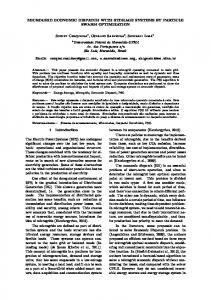
A Voltage-Source Inverter for Microgrid Applications with an Inner Current Control Loop and an Outer Voltage Control Loop Tine Vandoorn, Bert Renders, Frederik De Belie, Bart Meersman and Lieven Vandevelde Electrical Energy Laboratory (EELAB), Department of Electrical Energy, Systems and Automation (EESA), Ghent University, Sint-Pietersnieuwstraat 41, B-9000 Ghent, Belgium, Phone: +32 9 264 34 22, Fax: +32 9 264 35 82 e-mail:
[email protected]
Abstract Distributed generation (DG) units are commonly interfaced to the grid by using voltage-source inverters (VSI’s). Extension of the control of these inverters allows to improve the power quality if the main power grid is disturbed or disconnected. In this paper, a control technique is developed for a VSI working in island mode. The control technique is designed in the time domain, combining an inner current control loop with an outer voltage control loop. Voltage regulation under various linear and non-linear load disturbances is studied.
Keywords Microgrid, distributed generation, voltage control, current control
1.
Introduction
Recently, distributed generation (DG) units are increasingly being used because of their economical and environmental benefits compared to the use of large power plants. Many distributed power sources, such as most wind turbines, photovoltaics (PV) and fuel cells, do not generate a 50 Hz voltage, so they require a voltage-source inverter (VSI) as an interface to the grid. These power-electronic interfaces have different properties as compared to conventional power plants [1, 2]. DG systems with VSI’s are promising because of their possibility of high service reliability, power quality and flexibility, lower losses in transmission and distribution and a lower dependence on fuel costs when using renewable energy sources. The Consortium for Electric Reliability Technology Solutions (CERTS) presents a microgrid as a system providing both power and heat where most of the sources are connected to the ac-grid via power-electronic interfaces [3]. The microgrid architecture insures that the electrical impact of distributed energy resources (DER, [4]) on its bulk power provider at least qualifies the microgrid as a good citizen, meaning that it complies with grid rules. Potentially the microgrid behaves as a model citizen [1], meaning that inverter-based DG always acts to improve the local electrical environment.
microgrid
primary energy source
Filter + VSI
ig
iL iC C
vg
T1
T4
vsw T2
Vdc T3
Figure 1: VSI, interface between the microgrid and an energy source
DER can operate in parallel to the grid or islanded from it. The microgrid will disconnect from the main grid during large disturbances (voltage collapse, faults, poor power quality). In this paper, a microgrid in islanded mode with a single VSI-connected DG-unit is studied. The control of the VSI is usually obtained in the rotating dq-reference frame synchronous to the grid voltage, for example in [5–8]. An advantage of this method is that the i-th harmonic of the signals 50 Hz component can easily be evaluated using a lowpass filter after transformation to a reference frame rotating with i times the fundamental pulsation. A disadvantage of this method is the numerical complexity, because of, for example, the need for harmonic reference. By using the Clarke and Park transformations, the quantities in a threephase balanced sinusoidal system in steady state are transformed into dc-Park components, which is an advantage for control issues. However, in three-phase asymmetrical systems or in systems with voltage harmonics, the Park transformation does not result in dc-quantities. In singlephase systems, the Park or Clarke transformations are even not applicable. Therefore, in [9], a Kalman-filter technique is used for the transformation to values that match an ideal sinusoidal waveform as closely as possible, even if the voltage is highly distorted by the presence of harmonics. Those values are the inputs of a phase-locked loop (PLL) for transformation to the dq-reference frame and this ensures a fast and low distorted operation of the PLL.
vg∗
+
Voltage control
Current limit
i∗L
δff Vdc ∗ Current vsw + VSI control
Micro− grid
iL
ig
vg
Figure 2: VSI control scheme: schematic overview
In the current paper, the control is performed in the time domain without transformation of reference frame and by using conventional PI-regulators. A single-phase grid is studied and, in further research, this will be extended to a three-phase grid. The voltage of the grid is controlled by an inner current control loop and an outer voltage control loop. To constrain the inverter current within its safety limits, a fast current controller is used in the inner loop, having a reference current obtained by the outer-loop voltage regulation. An advantage of the inner current control loop is its easy current limit function. More advantages of the inner current control loop are described in [8].
2.
Control Strategy
In this paper, a control strategy for inverters in island mode is described, the topology of the VSI is shown in Fig. 1. In this figure the grid is represented as a load. The aim is to control both the amplitude and the frequency of the grid voltage vg (t). A schematic overview of the control strategy is shown in Fig. 2. In the fast inner current control loop, the measured inverter current iL (t) is compared with the set value i∗L (t) of this current. The obtained current error is presented to a discrete proportional-integral controller. The output of the current controller is the set value of the switching voltage ∗ (t) or, equivalently, the duty-ratio δ(t). To obtain betvsw ter disturbance rejection, a duty-ratio feed-forward branch is added to the output of the current controller [10]. The sum of the duty-ratio and the duty-ratio feed-forward is the input of the PWM-unit, which calculates the switching signals for the inverter. The design of the current controller is based on: L
diL (t) = vsw (t) − vg (t), dt
ˆ but also determined by variations of the control variable δ, by variations of the grid voltage vˆg and the inverter dc-bus voltage vˆdc . The latter two variations can be considered as disturbances. Implementing a duty-ratio feed-forward δff (t) decreases the influence of these disturbances [10]. This results in a better current tracking [11]. The duty-ratio feed-forward branch is given by δff (t) =
(4)
Using the following transfer function of duty-ratio to inverter current: ˆiL (s) Vdc = (5) ˆ sL δ(s) the inner PI-regulator can be tuned. The input of the inner PI-regulator is the measured current iL compared to its reference value i∗L . The output of this regulator is the desired duty-ratio δ of the PWM module. To obtain i∗L , the reference grid voltage vg∗ is compared to its measured value vg and controlled by a second PIregulator. The PI-regulator to control the grid voltage vg is tuned by using the transfer function 1 vˆg = ˆ sC ic
(6)
and a Pad´e approximation for delay time as a result of the sample and hold procedure. The output of the outer PIregulator is ∆i∗c , with ∆i∗c a small-signal deviation of i∗c . The input of the inner PI-regulator is ∆iL = i∗L − iL
(7)
and ∆iL consists of two parts: ∆iL = ∆iL,1 + ∆iL,2 .
(8)
In the previous equation ∆iL,1 = ∆i∗c using eq. (6) as ∆iL is changed in order to decrease the difference between vg and vg∗ . ∆iL,2 is an open-loop feed-forward of ∆iL or ∆iL,2 = ig + i∗c − iL .
(9)
The inner PI-regulator forces iL to its reference value. (1)
Another method to derive the transfer functions (5) and (6) is by using the state space model:
and vsw the switching voltage averaged over a PWM period, given by vsw (t) = δ(t).vdc , (2) with δ ∈ [−1, 1]. Further in this paper, the time dependence of the following functions will be taken implicitly. Transformation to a small signal model in the Laplace domain results in ˆ ˆiL (s) = Vdc δ(s) + δ0 vˆdc (s) − vˆg (s) , sL sL sL
vg (t) . vdc (t)
(3)
with δ0 the average duty-ratio and where hatted values x ˆ denote small deviations from the steady state value of x. This equation shows that the current of the inverter iL is
which gives: iL 0 d = 1 dt vg C
dx = Ax + Bu dt
(10a)
y = Cx + Du
(10b)
1 1 − iL L + L vg 0 0
0 vsw . 1 ig − C (11)
The PI-regulator must be robust for disturbances. The bandwidths of the two PI-regulators are different and the
Vdc
Cf
R
S4
Voltage Vg (V)
S1
L
RL
100
0 -100 -200 0
S2
Obtained Desired
200
0.02
0.04
0.08 0.1 Time (s)
0.06
S3
0.12
0.14
(a) Overview
Voltage Vg (V)
235
Figure 3: Resistive load: topology
different values of L and C cause different time constants between the two equations in (11). This results in a different dynamic behaviour between the two control loops, causing separation of the variables. The following transfer functions can be derived by using eq. (2) and (11): (12)
1 vˆg . = ˆ sC ic
(13)
(14)
The gradient of the linear approximation is obtained as: diL (t) diL (t) s2 C = s lim L ( ) = lim δVdc s→∞ s→∞ 1 + s2 LC t→0 dt dt (15) or δVdc diL (t) = (16) lim t→0 dt L lim
resulting in ˆiL Vdc = ˆ sL δ
(17)
which is analogous with eq. (5). By implementing a controller with two loops in series, an additional advantage is created as the inverter current iL can easily be limited.
3.
220 0.059
0.06 Time (s)
0.061
(b) Detail: amplitude error (peak of vg ) 8 6 4 2 0 -2 -4 -6 -8
0.0548
Obtained Desired
0.0549
0.055
0.0551 0.0552 Time (s)
0.0553
(c) Detail: phase error (zero-crossing of vg )
As the switching period of the PWM is at least ten times shorter than the time constant of transfer function (12), the response to a step input 1s in δ, viz an exponential function, di can be approximated as linear with gradient dt : diL (t) sC 1 ) = siL = s( δVdc ) . 2 dt 1 + s LC s
225
Voltage Vg (V)
sC iˆL = Vdc ˆ 1 + s2 LC δ
Obtained Desired
230
215 0.058
and
L(
0.18
0.16
Simulation Results
In the simulations, a sample frequency of 10 kHz is used. The unity gains of the PI-regulators are located at ωPIo = rad 3000 rad s and ωPIi = 8000 s for the outer and the inner regulator respectively. The dc-bus voltage Vdc equals 300 V and the desired grid rms voltage vg equals 163 V with a fundamental frequency of 50 Hz.
Figure 4: Resistive load: grid voltage vg with its reference value
A.
Resistive load
In a first simulation, the load has a resistance R of 25 Ω in series with the line resistance RL . The line resistance is Ω chosen at 0.411 km and the length of the line is 800 m, resulting in RL = 0.33 Ω. The microgrid topology is shown in Fig. 3. The simulation results of Fig. 4(a) show the obtained grid voltage vg and the reference grid voltage vg∗ . A detail of Fig. 4(a) is shown in Fig. 4(b) and Fig. 4(c). Both an error in amplitude and in phase difference is possible. The difference of the amplitude of the obtained voltage with respect to the desired voltage is shown in Fig. 4(b), only a small error is observed. The phase difference is shown in more detail in Fig. 4(c) where a zero-crossing of vg is shown, this error is negligible.
B.
Switching load
In a second simulation, the load consists of a load R of 25 Ω which halves after 0.06 s by switching a second resistance R2 of 25 Ω on after 0.06 s. The overall simulation results of the obtained grid voltage vg compared to the reference grid voltage vg∗ are analogous with Fig. 4(a), and a detail is shown in more detail in Fig. 5. The difference between the obtained and the desired voltage is more clear if t = 0.06 s as this is the switching instance, but, as shown in Fig. 5, the error is still small. The sampled inverter current iL is shown in Fig. 6. A small
Obtained Desired
230 225
2500 2000 Grid Power
Voltage Vg (V)
235
Active power (W) Reactive power (VA)
1500 1000 500 0
220
-500 0
215 0.058
0.059
0.06 Time (s)
0.02
Figure 5: Switching load: detail amplitude error in grid voltage vg
Current IL (A)
0.06
L
RL
20 10 0
R2
Obtained Desired
-10
0.12
0.14
0.16
0.18
S1
S4
Cf
R
Vdc
Ih
-20 0.01 0.02 0.03 0.04 0.05 0.06 0.07 0.08 0.09 Time (s)
0.08 0.1 time (s)
Figure 8: Switching load: grid active and reactive power (vg and ig )
30
-30 0
0.04
0.061
0.1
S2
Figure 6: Switching load: sampled inverter current iL with its reference value
S3
Figure 9: Harmonic load: topology
235
10
0 -10 -20 0
0.01
0.02
0.03
0.04
0.05 0.06 T ime (s)
0.07
0.08
0.09
0.1
Voltage Vg (V)
Cirrent Ig (A)
20
Obtained Desired
230 225 220 215 0.058 0.0585 0.059 0.0595
Figure 7: Switching load: grid current ig
0.06 0.0605 0.061 0.0615 Time (s)
Figure 10: Harmonic load: detail amplitude error in grid voltage vg transient behaviour can be concluded from this figure. The inverter current iL equals ic + ig and the switching ripple in iL is almost completely absorbed in the capacitor current ic . The current ig is shown in Fig. 7, its peak current before the switching instant is approximately 9.2 A and, as expected, this is doubled (18.4 A) by halving the load resistance. Also, when comparing ig to iL a phase-difference is obtained as the capacitor injects a reactive current into the grid. Before the transient the active power exported to the grid equals 2 vg,rms = 1.058 kW, R
(18)
after 0.06 s the active power equals 2 vg,rms = 2.116 kW. 0.5R
(19)
C.
In the next simulation, the load consists of the previous load R of 25 Ω. This resistance is connected in parallel with a current source which is placed in series with a second resistance R2 of 25 Ω as shown in Fig. 9. The current source has an amplitude of 5 A and a frequency of 250 Hz. The simulation results of the obtained grid voltage vg and the reference grid voltage vg∗ is shown in detail in Fig. 10 and the overview is analogous with Fig. 4(a). The error of the obtained voltage compared to the desired voltage is small. The sampled inverter current iL contains a fifth harmonic component next to the fundamental component, as shown in Fig. 11.
D. The grid active and reactive power, calculated with the active & reactive power block of MatLab SimPowerSystems, are shown in Fig. 8.
Harmonic load
Robustness
In this paragraph, the robustness to measurement inaccuracy and parameter faults is studied.
20
10
0
Desired Obtained
-105
0.01
0.02
0.03
0.04
0.05 0.06 T ime (s)
0.07
0.08
0.09
0
-20
0.1
0.045
Figure 11: Harmonic load: sampled inverter current iL with its reference value
0.05
0.055 Time (s)
0.065
0.06
Figure 13: White noise: sampled inverter current iL with its reference value
200
235
100
0
-100-
Desired Obtained
-200 0
0.01
0.02
0.03
0.04
0.05 0.06 T ime (s)
0.07
0.08
0.09
0.1
Voltage Vg (V)
Voltage Vg (V)
Desired Obtained
10
-10
-20 0
Current I L (A)
Current IL (A)
20
225 220 215 0.058
(a) Overview 235
Obtained Desired
230 225
0.059
0.06 Time (s)
0.061
Figure 14: Robustness: Detail, amplitude error in grid voltage vg
220 215 0.058
0.059
0.06 Time (s)
0.061
0.062
(b) Detail: amplitude error
40 Current IL (A)
Voltage Vg (V)
Obtained Desired
230
Measurement inaccuracy: white noise
In the next simulation, the load consists of the previous harmonic load of Fig. 9. A band-limited normally distributed noise is added to the inverter current iL in order to simulate measurement error. The maximum value of this noise is 1 A. The simulation results of the obtained grid voltage vg compared to the reference grid voltage vg∗ are shown in Fig. 12(a) and Fig. 12(b). The difference between the obtained and the desired voltage is more clear than in the previous simulations. A maximum deviation of 1.5 V or 0.6 % compared to the peak voltage of 230 V is obtained resulting in a non-significant error in the simulations. In the sampled inverter current iL a fifth harmonic caused by the load is obtained next to the ground wave, as shown in Fig. 13, where one fundamental period of 20 ms is shown. The error of the obtained current compared to the desired current increases under increasing measurement noise. The disturbance rejection of the inner loop is sufficient. The inner loop is fast in comparison with the outer voltage loop which results in an even better disturbance rejection of the outer loop.
2)
Parameter faults
In this simulation, the load consist of the previous harmonic load of Fig. 9. The real filter capacitor C equals
0 -20 -40 0
Figure 12: White noise: grid voltage vg with its reference value
1)
Desired Obtained
20
0.01
0.02
0.03
0.04 T ime (s)
0.05
0.06
0.07
Figure 15: Robustness: sampled inverter current iL with its reference value
125 µF. The regulators are incorrectly tuned with C = 250 µF, i.e. a 100 % mismatch. The simulation results of the obtained grid voltage vg and the reference grid voltage vg∗ are shown in detail in Fig. 14, and the overview is analogous to Fig. 12(a). The difference between the obtained and the desired voltage is small, so it can be concluded that the robustness of the PI-regulators is sufficient. In the sampled inverter current iL a fifth harmonic caused by the load is obtained next to the ground wave, as shown in Fig. 15, it is shown that the parameter sensitivity is sufficiently low.
4.
Conclusions
The control of the voltage of a single-phase microgrid with one VSI is obtained. This control has two separate control loops: a voltage control loop and a fast current control loop. The output of the voltage control loop is the input of the current control loop, using separation of variables. The control is studied under different loads, transient effects and other disturbances resulting in a robust control strategy
with sufficiently low parameter sensitivity. An advantage of this approach is that it can be adopted to control both single- and three-phase microgrids. In future work microgrids with multiple VSI’s will be considered.
Acknowledgement This research of Tine Vandoorn is funded by the Special Research Fund (BOF) of Ghent University. The research was carried out in the frame of the inter-university Attraction poles IAP-VI-021, funded by the Belgian Government.
References [1] T. Green and N. Pogaku, “A model citizen approach to integrating inverter-based distributed generation.” World Renewable Energy Congress (WREC), 2005, pp. 1101–1108. [2] E. Barklund, N. Pogaku, M. Prodanovi´c, C. HernandezAramburo, and T. C. Green, “Energy management in autonomous microgrid using stability-constrained droop control of inverters,” IEEE Trans. Power Electron., vol. 23, no. 5, pp. 2346–2352, Sept. 2008. [3] R. H. Lasseter, A. Akhil, C. Marnay, J. Stephens, J. Dagle, R. Guttromson, A. Meliopoulous, R. Yinger, and J. Eto, “The CERTS microgrid concept, white paper on integration of distributed energy resources.” California Energy Commission, Office of Power Technologies - U.S. Department of Energy, Apr. 2002. [4] D. Moskovitz, “Profits and progress through distributed resources.” Regulatory Assistance Project, Tech. Rep., Feb.
2000. [5] M. Prodanovi´c and T. C. Green, “High-quality power generation through distributed control of a power park microgrid,” IEEE Trans. Ind. Electron., vol. 53, no. 5, pp. 1471– 1482, Oct. 2006. [6] N. Pogaku and T. Green, “Harmonic mitigation throughout a distribution system: a distributed-generator-based solution,” IEE Proc. Gener. Transm. Distrib., vol. 153, no. 3, pp. 350–358, May 2006. [7] R. Teodorescu and F. Blaabjerg, “Flexible control of small wind turbines with grid failure detection operating standalone and grid-connected mode,” IEEE Trans. Power Electron., vol. 19, no. 5, pp. 1323–1332, Sept. 2004. [8] M. Prodanovi´c, “Power quality and control aspects of parallel connected inverters in distributed generation,” Ph.D. dissertation, University of London, Imperial College, 2004. [9] K. De Brabandere, T. Loix, K. Engelen, B. Bolsen, J. V. Keybus, J. Driesen, and R. Belmans, “Design and operation of a phase-locked loop with kalman estimator-based filter for single-phase applications,” in Conf. of the IEEE Ind. Electron. Society (IEEE IECON’06), Paris, France, pp. 525–530, Nov. 7-10, 2006. [10] D. M. Van de Sype, K. De Gussem´e, A. P. M. Van den Bossche, and J. A. Melkebeek, “Duty-ratio feed-forward for digitally controlled boost PFC converters,” IEEE Trans. Ind. Electron., vol. 52, no. 1, pp. 108–115, Feb. 2005. [11] B. Renders, K. De Gussem´e, W. R. Ryckaert, and L. Vandevelde, “Input impedance of grid-connected converters with programmable harmonic resistance,” IET Electr. Power Appl., vol. 1, no. 3, pp. 355–361, May 2007.