algorithm that results in 3.5X to 5.5X speedup over state-of-the- art FPGA ... performance evaluation of LDPC codes is very desirable to de- sign better codes for these ..... in python to automate the creation of vector decoder archi- tecture.
Accelerating FPGA-based Emulation of Quasi-Cyclic LDPC Codes with Vector Processing Xiaoheng Chen, Jingyu Kang, Shu Lin and Venkatesh Akella Department of Electrical and Computer Engineering University of California Davis, California 95616, USA Email: {xhchen, jykang, shulin, akella}@ucdavis.edu
Abstract—FPGAs are widely used for evaluating the error-floor performance of LDPC (low-density parity check) codes. We propose a scalable vector decoder for FPGA-based implementation of quasi-cyclic (QC) LDPC codes that takes advantage of the high bandwidth of the embedded memory blocks (called Block RAMs in a Xilinx FPGA) by packing multiple messages into the same word. We describe a vectorized overlapped message passing algorithm that results in 3.5X to 5.5X speedup over state-of-theart FPGA implementations in literature.
I. I NTRODUCTION LDPC codes, discovered by Gallager in 1962 [1], were rediscovered and shown to approach Shannon capacity in the late 1990s. Today LDPC codes are being considered for a wide variety of emerging applications such as high-density flash memory, satellite broadcasting and mobile WiMAX. Rapid performance evaluation of LDPC codes is very desirable to design better codes for these applications. For some applications (such as storage systems), it is necessary to prove the absence of error-floor down to 10−12 which is almost impractical on a conventional CPU. As a result, FPGAs are being widely used to emulate the performance of LDPC codes. Zhang et. al [2], [3] and [4] proposed techniques to realize partially parallel architectures to implement LDPC decoders efficiently on an FPGA. As a result, FPGAs are being widely used to emulate the performance of LDPC codes. Recently, researchers at Berkeley [5], [6], [7] describe a Virtex-II Pro based hardware emulation platform LDPC decoders. Saunders et. al [8] merge multiple messages into a single SISO message to save total memory bits of FPGA. As described in the next section, the message passing algorithm [9] is often used to decode the LDPC codes. Variable-to-check messages and check-to-variable messages are computed by variable nodes and check nodes processing units and are passed along the edges in the Tanner graph. One iteration of message passing contains two steps: check node update and variable node update. The two steps can be overlapped to increase decoding throughput, which is referred to as overlapped message passing (OMP) [4], [10]. The conventional scheduling without overlapping the two steps is referred to as non-OMP method. In a FPGA-based implementation of the message passing algorithm (both OMP and non-OMP methods), the variable to check node and check node to variable node messages are stored in the embedded
978-3-9810801-5-5/DATE09 © 2009 EDAA
memory blocks, called Block RAMs in a Xilinx FPGA. We call these scalar decoders because a single message is stored in each Block RAM word. Scalar decoders do not take the full advantage of the high bandwidth capability of Block RAMs in modern FPGA, especially given that typically messages do not require more than 5 or 6 bits of precision [2]. For example, in a Virtex-5 FPGA, Block RAMs can have 18, 36, or 72 bit wide ports, which means that a scalar implementation potentially waste a significant fraction of the available memory bandwidth. In this paper, we propose a technique called VMP (vector message passing) that treats the wide word in a Block RAM as a short vector, that holds multiple messages, which are loaded and stored simultaneously. VMP introduces new challenges for data packing and alignment which can be solved by taking advantage of the configurable logic resources of an FPGA. This allows us to build a customized vector processor for a given LDPC code and desired data precision to improve the decoding throughput over conventional scalar decoders. However, this improvement comes at the expense of additional logic resources (flip-flops and slices) to implement the additional functional units to support vector processing and the required data alignment and addressing. For large LDPC codes this might result in a given decoder not fitting inside an FPGA. So, a careful design space exploration is needed to select the appropriate vector length for VMP, to maximize the decoding throughput given the resource constraints of the FPGA available for emulation. We built a tool, called QCSyn, to facilitate the exploration of the design space of vector LDPC decoders on a given FPGA platform. QCSyn is used to derive the results described in this paper. The rest of the paper is organized as follows. We start with an overview of the design, construction, and decoding of QCLDPC codes using the iterative message-passing algorithm. This is followed by the details of the vector decoding architecture and the VMP algorithm. We conclude with the results of our implementation and directions for future work. II. QC LDPC C ODES A. Code Construction A (γ, ρ) binary quasi-cyclic (QC) LDPC code is defined as the null space of a sparse parity-check matrix H over GF(2) with the following structural properties: (1) each row has
constant weight (regular) or multiple weights no greater than ρ (irregular). (2) each column has constant weight (regular) or multiple weights no greater than γ (irregular). (3) no two rows (or two columns) can have more than one position where they both have 1-components. (4) the H matrix is composed of γ × ρ block matrices showed below: A0,0 A0,1 ··· A0,ρ−1 A1,0 A1,1 ··· A1,ρ−1 H= .. .. .. . . . . . . Aγ−1,0 Aγ−1,1 · · · Aγ−1,ρ−1 where Ai,j refers to either a m × m all-zero matrix or a circulant permutation matrix (CPM) for 0 ≤ i ≤ γ − 1 and 0 ≤ j ≤ ρ − 1. A CPM is a circularly shifted identity matrix with certain offset. The size of the H matrix is (γm) × (ρm). The code rate is no less than 1 − (γ/ρ). Binary QC LDPC codes are constructed based on algebraic and combinatorial tools, such as finite geometries, balanced incomplete block designs, Reed-Solomon codes with two information symbols, and finite fields [11]. The density of an H matrix can be reduced by replacing a set of CPMs by zero matrices. The replacement of CPMs with zero matrices is referred to as masking [11]. Masking results in a new array whose Tanner graph has fewer edges and hence has fewer short cycles and possibly larger girth. m = 31
1
2
4
8
16
5
10
20
9
18
25
19
7
14
28
m
2
v ∈N (c)\v
v 0 ∈N (c)\v
STEP 3 Variable node update: At variable node 0 ≤ v < ρm − 1, for 0 ≤ c ≤ γm − 1, compute qvc and zv by X qvc = yv + σc0 v c0 ∈M(v)\c
offset = 2 Fig. 1.
this problem, the normalized min-sum algorithm (NMSA) was introduced [12] and shown to be a better approximation of SPA. Besides, NMSA does not need any channel statistics. Therefore, we use NMSA for evaluating the performance of LDPC codes. A QC-LDPC code defined by a H matrix size of (γm×ρm) has ρm bits per codeword and γm parity checks checking the code bits. In the Tanner graph of a QC LDPC code, each bit is represented by a variable node and each parity check is represented by a check node. An edge exists between the variable node v and the check node c if hcv = 1 in the H matrix. Let the set M(v) denote the set of check nodes connecting the variable node v. Let the set N (c) denote the variable nodes connected to the check node c. Let y = (y0 , y1 , · · · , yρm−1 ) be the soft-decision received sequence at the input of the decoder. Let z = (z0 , z1 , · · · , zρm−1 ) be the posterior softdecision information. At the i-th iteration, for 0 ≤ c < γm and 0 ≤ v < ρm, let qvc and σcv be the message from variable node v to check node c and the message from check node c to variable node v. In every iteration, the variable-to-check messages and the check-to-variable messages are updated. The normalized min sum algorithm is presented below. STEP 1 Initialization: Set i = 0 and the maximum number of iterations to Imax . Set qvc = yv . STEP 2 Check node update: at check node 0 ≤ c ≤ (i) γm − 1, for 0 ≤ v < ρm − 1, compute σcv by Y σcv = α · 0 min |qcv0 | · sign (qcv0 )
Code structure of a (3,5) regular QC-LDPC code
Figure 1 shows the code structure of a (3, 5) regular QCLDPC codes. The H matrix has 3 block rows and 5 block columns. Each block matrix is a 31 × 31 CPM with certain offset displayed in the square symbol. The concept of CPM is further explained by a CPM with offset 2. The entries along the dashed line of the CPM are 1, while other entries are 0.
zv
= yv +
X
σcv
c∈M(v)
STEP 4 Tentative decode: If sign (z) · HT = 0 or Imax is reached, go to (5). Otherwise, i ← i + 1 and go to (2). STEP 5 Termination: Take sign (z) as the decoded codeword and stop the decoding process. III. V ECTOR D ECODER FOR QC LDPC C ODES A. Decoder Architecture Overview
B. Message Passing Decoding An LDPC code can be decoded under iterated message passing algorithm for Shannon capacity approaching error performance. The sum-product algorithm (SPA) and loglikelihood-ratio (LLR)-based SPA gives the best performance among soft-decision decoding. However, they require complex computations including nonlinear functions. An approximated version of LLR-SPA, called the min-sum algorithm (MSA) [12] requires less decoding complexity at the expense of some performance degradation. However, for LDPC codes with large check node degrees, the performance degradation of MSA compared to SPA could be as large as 1 dB. To address
In a FPGA-based partially parallel QC-LDPC codes decoder, the intrinsic messages (y in NMSA), extrinsic messages (qvc , σcv ) and hard decision bit (sign(z) in NMSA) are grouped based on CPM locality and mapped to embedded memory (Block RAMs in Xilinx). A modulo counter is associated with each memory to generate the corresponding memory address, which always counts from certain initial value and then wraps around to the starting address. (γ + 2) embedded memory are required for a regular (γ, ρ) QC-LDPC code decoder, among which γ × ρ memory are used for extrinsic messages, ρ memory are used for intrinsic messages, and ρ memory are used for hard decision bit. To differentiate from
the proposed vector decoder, we name refer to this as a scalar decoder. Given that the scalar decoder uses a memory word to store one message, only one message can be read out or written per memory access.
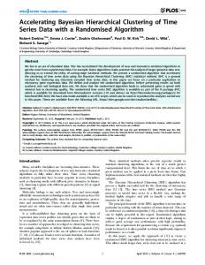
CNU
CNU
CNU
Fig. 2.
E0,0
E0,1
E0,2
E0,3
E0,4
E1,0
E1,1
E1,2
E1,3
E1,4
E2,0
E2,1
E2,2
E2,3
E2,4
VNU
VNU
VNU
VNU
VNU
I0
I1
I2
I3
I4
A vector decoder for code depicted in figure 1 when K = 2
B. Message Packing and Alignment
VNU Write Alignment
0 1
0 4
3 7
29 2
30 3
0 4
1 5
...
...
...
...
...
...
CNU
2 6
...
29 30
1 5
CNU Write Alignment
...
...
We exploit the wider bitwidth and configurability of embedded memory blocks to propose a vector decoder architecture. For example, in a Xilinx Virtex FPGA, a 18K Block RAM (BRAM) can be configured in different aspect ratios such as 8k 2-bit words or 512 36-bit words. For normalized min sum algorithm, the intrinsic and extrinsic message is usually 68 bit wide, thus up to six 6-bit messages can be packed in one memory word in the 512 36-bit aspect ratio. We define the number of messages packed into one memory word as K. Figure 2 shows a vector decoder for our example (3,5) code when K = 2. CNU denotes the check node unit, which perform the check node update and parity check (Step 2 and Step 4 in NMSA). VNU denotes the variable node unit, which perform the variable node update (Step 3 in NMSA). I denotes the intrinsic memory, which stores the intrinsic messages. E denotes the extrinsic memory, which stores the extrinsic messages and hard decision bit. The hard decision bit is computed by VNU and appended at the head of the variableto-check messages. The vector decoder for a regular (γ × ρ) code requires K × γ CNUs, K × ρ VNUs, and (γ + 1) × ρ embedded memory. The decoding steps in NMSA are mapped to the vector decoder architecture as below. STEP 1 Initialization Load the received intrinsic messages to both the ρ intrinsic message memory I and the γ × ρ extrinsic message memory E. K × ρ messages are load at one clock cycle. STEP 2 Check node update and tentative decode: The K × γ CNUs read the variable-to-check messages and update the check-to-variable messages simultaneously. Each CNU read ρ messages from ρ extrinsic memory of the same block row. For example, the 1st and the 2nd CNUs read messages from and update messages to extrinsic memory E0,0 , E0,1 , E0,2 , E0,3 , E0,4 in Figure 2. Besides, the CNUs extract hard decision bits from the variable-to-check messages and check the parity. STEP 3 Variable node update: The K × ρ variable node
units (VNUs) read the intrinsic messages and the check-tovariable messages, and update the variable-to-check messages simultaneously. Each VNU read γ messages from γ extrinsic memory of the same block column. For instance, the 3rd and the 4th VNUs read messages from I1 , E0,1 , E1,1 , E2,1 and update the corresponding messages in Figure 2. STEP 4 Termination: The hard decision bits are extracted from the extrinsic memory at the same block row and stored to data sink. The vector decoder architecture outperforms the scalar decoder in two ways. First, the embedded memory port can be configured wide to read and write multiple message per port access without sacrificing clock frequency, thus we can exploit higher memory bandwidth for throughput gain by incorporating K-times processing units. Second, the vector decoder embeds the hard decision bits in the variable-to-check messages, and thus save ρ embedded memory and routing resources.
24 28
25 29
26 30
27
22 26
23 27
24 28
25
CNU
CNU
CNU
CNU
VNU
VNU
VNU
VNU
VNU
CNU Memory (a) K=1
VNU Memory (b) K=4
Fig. 3. Message packing when K = 1 and K = 4 for CPM depicted in figure 1
In the scalar decoder, which is same as a vector decoder with K = 1, a message is packed in one memory word. The memory structure can be modeled as a one dimensional array L[m], as shown in Figure 3(a). For simplicity, all the indices, addresses, and pointers are assumed to start at 0. The message is packed in the row major order of the CPM, i.e., the message in the i-th CPM row is packed in L[i]. The location for message L[i] stores σcv at step (2) and qvc at step (3), i.e., the extrinsic messages are updated in place. For standard decoding scheduling, the CNU starts from the 0-th CPM row, i.e., in the order of L[0], L[1], · · · , L[m − 1]. The VNU starts from the 0-th CPM column, i.e., in the order of L[m − offset], · · · , L[m − 1], L[0], · · · , L[m − offset − 1]. For the vector decoder architecture, K > 1 messages are packed in one memory word. We use double buffering technique to eliminate memory conflict for CNU and VNU access. The extrinsic memory is divided into two parts: one for CNU to read out and VNU to write into (denoted as CNU memory), another for VNU to read out and CNU to write into
(denoted as VNU memory). Although double memory is being used, it does not change the number of Block RAMs used, which is important because the key limitation to the size of the LDPC code that can be accommodated on a given FPGA is limited by the number of Block RAMs not the memory capacity. When K > 1, each CNU or VNU memory has dm/Ke memory words and K messages per word. The CNU and VNU memory can be modeled as two dimensional arrays, denoted by Lc and Lv . Figure 3(b) shows the packing details for a CPM with m = 31 and offset 2 when K = 4. The variable-tocheck messages are packed in the CNU memory by the CNU access order, i.e., the message L[0] is packed as Lc [0][0]. The check-to-variable messages are packed in the VNU memory by the VNU access order, i.e., the message L[m − offset] is packed as Lv [0][0]. Generally, the message L[k] is packed to the location Lc [bk/Kc][k mod K] in the CNU memory and Lv [b((k+offset) mod m)/Kc][((k+offset) mod m) mod K] in the VNU memory. As L[k] is mapped to different locations in the CNU memory and VNU memory except when offset = 0, the messages need to be aligned before they are written into the memory. As shown in Figure 3(b), messages L[0], L[1], L[2], L[3] are read out and processed by four CNUs simultaneously. However, L[0], L[1] and L[2], L[3] are aligned by CNU Write Alignment unit and written into different memory words in the VNU memory. Besides, when L[0] is not mapped to the 0th column of the VNU memory, or L[m − offset] is not packed in the 0th column of the CNU memory, the starting row for write will be accessed twice. For instance, the 0th row of the VNU memory in Figure 3(b) will be accessed twice in the check node update step, since L[29], L[30] and L[0], L[1] are packed into the same row. The CNU Write Alignment and VNU Write Alignment units are implemented using registers and multiplexors.
overlapped message passing (VMP) scheme to exploit the vector processing architecture. Let w ˜ denote the number of waiting clock cycles between CNU update and VNU update of the same iteration. We minimize w ˜ as below. (1) Apply the OMP method: Let c = {c0 , c1 , · · · , cγ−1 } denote the starting CPM rows for CNUs. Let v = {v0 , v1 , · · · , vρ−1 } denote the starting CPM columns for VNUs. Let w denote the waiting time between intra-iteration CNU and VNU computations. We apply the OMP method described in [10] to get c, v, and w. (2) Message packing: We use the same memory model and notation system described in the previous subsection to explain the packing scheme. For an extrinsic memory Ei,j , the CNU starts from the CPM row ci , and the VNU starts from the CPM column vj . The variable-to-check messages are packed in the CNU memory by the CNU access order, i.e., the message L[ci ] is packed as Lc [0][0]. The check-to-variable messages are packed in the VNU memory by the VNU access order, i.e., the message L[vj − offset mod m] is packed as Lv [0][0]. Generally, the message L[k] is packed to the location Lc [b(k − ci )/Kc][(k − ci ) mod K] in the CNU memory and to Lv [b((k − vj + offset) mod m)/Kc][((k − vj + offset) mod m) mod K] in the VNU memory. (3) Compute the starting read and write word address at the 1st iteration. The starting CNU or VNU read address is 0. The starting write message for CNU is L[ci ], which is packed in Lv [xc (i, j)][yc (i, j)] in the VNU memory, where xc (i, j) = b((ci − vj + offset) mod m)/Kc yc (i, j) = ((ci − vj + offset) mod m) mod K Likewise, the starting write message for VNU is L[vj − offset mod m], which is packed in Lc [xv (i, j)][yv (i, j)] in the CNU memory, where xv (i, j) yv (i, j)
C. Vector Message Passing 1st iteration
(4) Compute the minimum waiting time for VMP by
2nd iteration
CNU
VNU
CNU
1st iteration
2nd iteration
VNU
...
(a) Non-OMP, K=1
CNU
VNU
CNU
VNU
n-th iteration
...
CNU
VNU
(b) Vector Non-OMP, K=2
w
1st iteration
CNU
CNU VNU
... VNU
2nd iteration
w
CNU ...
VNU n-th iteration
(c) OMP, K=1 1st iteration
CNU VNU ~ w
~ w CNU VNU
... ...
2nd iteration
CNU VNU n-th iteration
(d) Vector OMP, K=2
Fig. 4.
= b(vj − ci − offset) mod m)/Kc = (vj − ci − offset) mod m) mod K
Comparison of Scheduling Schemes
Overlapped message passing (OMP) method was proposed by [4] and further optimized by [10] to reach the maximized concurrency and avoid memory access conflicts. As showed in Figure 4(a,b), the non-OMP-based vector decoder reduces sub-iteration time by vector processing, and thus increases throughput. Based on the OMP method, we propose a vector
w ˜=
max
0≤i