voltage. In Ref. [2] an analog circuit was designed in order to compensate for this non-linearity .... By zero correcting both the meter reading and the ramp rate we.
Accurate Sub-picoampere Current Source Based on a Differentiating Capacitor with Software-controlled Non-linearity Compensation Helko E. van den Brom, Pieter de la Court, and Gert Rietveld
NMi Van Swinden Laboratorium, P.O. Box 654, 2600 AR Delft, The Netherlands
Abstract – A high accuracy current source has been developed for the generation of very small currents (below 200 pA) based on applying a linear voltage ramp to a capacitor. Using software-controlled compensation for the non-linearity of the voltage ramp, a stable current can be reached within a few seconds. A voltage ramp within typically 10·10-6 of any desired value between less than 1 mV/s and several hundreds of mV/s can be realized. Using a high quality air-dielectric capacitor, currents below 200 pA can be generated with an uncertainty of 20 µA/A (k=2), with a lower limit of 2.0 aA (k=2). Index terms – current source, capacitance, standard capacitor, calibration, picoammeter. I. INTRODUCTION The usual way of measuring small electrical currents employs an operational amplifier (opamp) with a high value feedback resistor. However, for currents well below 100 pA another method becomes more accurate, because high-ohmic resistors are not very stable and are difficult to calibrate. This is the so-called integrator method, where the current under investigation is used to charge a known capacitor, over which one can measure the voltage increase generated per unit of time. This integrator approach can be reversed in order to generate small electrical currents: when a voltage linearly increasing in time is applied to a capacitor, it differentiates this voltage into a DC current. The best way to generate a linear voltage ramp is to use an auxiliary integrator that integrates a relatively large current across a capacitor [1] (see Fig. 1). In order to generate a constant DC current, the applied voltage ramp must be very linear. In practice, however, the non-ideal behavior of the capacitor in the auxiliary integrator results in non-linearity of the ramp voltage. In Ref. [2] an analog circuit was designed in order to compensate for this non-linearity. In this paper we present a software-controlled non-linearity compensation method that is based on the same principle as in [2], but has the significant additional advantages of improved uncertainty, speed and flexibility. First, the principle of operation and the compensation method are described. Then, experimental results for the generation of very small currents with high accuracy are presented. Finally, the use of the current source is demonstrated in the calibration of a commercial picoammeter.
II. THE DIFFERENTIATING CAPACITOR CURRENT SOURCE A. Principle of operation The differentiating capacitor current source uses a capacitor (C’ in Fig. 1), connected in series with a linear ramp voltage generator (dV/dt = constant). As long as the voltage at the output of the capacitor remains constant (not necessarily zero), a current will flow through the capacitor with magnitude I = C ·(dV/dt) .
(1)
The principal disadvantage is that there are practical limits to the amplitude of the voltage ramp. At a given rate dV/dt, the voltage can be increased only for a limited time, after which the ramp direction must be reversed or stopped. It is possible to generate accurate voltage ramps from -10 V to +10 V in a time period from typically 100 to 2000 seconds or more, which practically results in a current range of around 200 pA or lower, using a 10 pF, 100 pF or 1000 pF series capacitor. Eq. (1) shows that for accurate currents, an accurate voltage ramp and a well-known capacitor are required. The output voltage of the ramp generator is measured by a calibrated long scale digital voltmeter (DVM), which is triggered by a precision time base. Subtracting consecutive voltage readings ∆V and dividing by the trigger interval
∆t the ramp rate ∆V/∆t is obtained. A high quality air-dielectric capacitor is generally believed to have a DC capacitance value equal within 10 µF/F to the value at the normal measurement frequency around 1 kHz, because the main AC/DC dependence of a capacitor is caused by the dielectric between the electrodes. The required further investigations to confirm this assumption fall outside the scope of this paper. B. Practical circuit Fig. 2 shows a schematic representation of our complete set-up. On the left hand side the auxiliary integrator can be seen, with an extra input for the compensation signal. The opamp used in our set-up is a low noise precision type with a JFET input stage, which has a negligible input current. With input currents in the order of microamps, the integrating capacitor Cint cannot be an air-dielectric capacitor due to the large value that is required (around 2 µF). All available capacitors suffer from non-ideal behavior, the most serious shortcomings being temperature dependence of the capacitance value, leakage resistance and dielectric absorption. Temperature influences are
minimized by placing Cint and the input resistor Rin in a separate, thermally insulated enclosure, where the heat generated by the opamp does not penetrate. The input offset voltage of the opamp is also temperature dependent and can have some influence on the linearity of the output voltage ramp. This effect is reduced by enclosing the opamp in another insulated box and minimizing the load current from the output. Choosing a Teflon type capacitor minimizes the effect of leakage resistance and dielectric absorption. Nevertheless, the non-ideal behavior is noticeable and needs to be compensated. In addition to the integrator circuit and the air-dielectric capacitor, the complete design (not shown in Fig. 2) includes some input filters, a low noise ±15 V supply with a doubly shielded power transformer, a limiter circuit that prevents the integrator output from running beyond ±11 V, and a simple resistive voltage divider, decreasing the output voltage by a factor of 1, 10 or 100. This way, very low ramp rates can be reached. The ratios of the divider need not be known very accurately since the voltage is measured at its output. C. Compensation method The non-ideal behavior of the integrating capacitor results in non-linearity of the ramp voltage. It is possible to improve the linearity significantly by injecting a compensation signal into the integrator circuit. Willenberg et al. [2] reported an analog feedback network that was found to work well. However, in order to cover the desired range of output currents, two different compensation circuits had to be designed, because the non-linearity appeared to be dependent on the capacitance value as well as on the input current of the auxiliary integrator. Therefore we decided to use a software-controlled correction signal that is automatically adapted to approach the ideal linear ramp by means of an iterative process. In our design a fixed ramping sequence (hold, ramp up, hold, ramp down) is generated and repeated a number of times, whereby the user can specify the number of sequences, ramp rate, ramp time and hold time (see Fig. 3). The software calculates the constant voltage Vin to match the required ramp rate and controls the DAC output 1 to switch between zero and the calculated voltage in the right polarity. The first run is done without any compensation, although in principle the correction signal determined in an earlier experiment could also be used. The output voltage of the ramp generator is measured with a DVM with a trigger interval and corresponding averaging time that can be set by the user to get a convenient number of voltage samples over the total ramp time. For each trigger the voltage
difference per time interval ∆V/∆t is compared with the desired ramp rate. The deviations are calculated and used to compute a pattern of compensation values as a function of time that are applied using DAC output 2 during the next sequence. Also during the hold periods, the output voltage changes are measured and compared with the desired value, which is zero in this case. The compensation method works equally well in this situation. In all sequences following the first run, the main input signal into the integrator Vin (on DAC output 1) remains constant, while the calculated compensation signal Vcorr (on DAC output 2) is adjusted with each trigger pulse. The resolution of the correction values is extremely high, by choosing Rcorr = 1000·Rin. Some low pass filtering is done at the integrator inputs to smooth the input signals, so that the step-wise changes of the correction voltage do not become significant in the output voltage ramp. In calculating the compensation values, a median filter and a moving average filter are used in order to suppress the increasing noise due to the adaptive compensation. During each sequence the measured ramp pattern is again compared with the ideal pattern and the compensation values are updated. This results in an iterative process that converges very quickly to the ideal ramping pattern. The residual deviations in the output voltage pattern are due to noise and any changes in the components from one sequence to the next, due to, for example, temperature changes. The significant advantage of this adaptive compensation method is that it does not depend on any modeling of the non-ideal behavior of the integrator circuit, but only on the assumption that the circuit characteristics are reasonably constant in time. Therefore, a continuous range of voltage ramps with corresponding currents can be generated. III. EXPERIMENTAL RESULTS A. The voltage ramp There are limits to the response of the compensating signal. In practice we found that it takes about 10 seconds after the start of the ramp to approach the set ramp rate of 100 mV/s to within 10·10-6 of the desired value, which is also about the final stability during the remainder of the ramp (see Fig. 4). For lower ramp rates dV/dt the relative final stability is worse, because the same fluctuations in the readout of the voltmeter V(t) are now taken relative to a smaller difference ∆V=V(t)-V(t-∆t). The main reason for the deviation from the ideal ramp in the first few seconds of the ramp is the step response of the Vin input filter and the digital filtering performed in the software. When using the current source for calibrations, for each ramp one has to skip the first 10 to 30 seconds in order to get rid of this
switching effect. In principle the filter could be optimized to attain the desired ramp rate in a shorter period. However, this is not necessary, for presently still sufficient measurement time remains. The iterative process converges to the intended ramping pattern typically within three repetitions (see Fig. 4). B. The differentiating capacitor current source In typical calibrations, the sequence of ramp patterns is repeated 10 to 50 times, whereas the number of points per ramp is 200, making the total duration about 2 to 10 hours per current value. For each sequence a positive and a negative ramp rate is determined. The leakage resistance of the charged capacitor will cause the current to drift slowly. This is because during a ramp, the voltage over the capacitor is changing typically from –10 V to +10 V. Combined with a leakage resistance of typically 1017 Ω this results in a leakage current changing from –100 aA to +100 aA during the ramp. For each part of the sequence (see Fig. 3), the first 10 to 30 points that are needed to approach the stable ramp rate are skipped. By also skipping the last 10 to 30 points the ramp pattern is symmetric around zero volts across the capacitor. Therefore, the influence of the leak resistance of the capacitor will be averaged out, reducing the corresponding uncertainty contribution by at least a factor of 10. The type A evaluation of the uncertainty is based on the results per ramp as described in the previous paragraph. We have studied the influence of varying the number of ramps as well as the number of points per ramp on the standard deviation of the mean. It turns out that increasing the number of points per ramp above 200 does not significantly reduce the standard deviation of the mean. Increasing the number of ramps averages out the fluctuations between the ramps, but leads to very long measurement times. In addition, day-to-day variations are often larger than the standard deviation of the mean in one measurement run, e.g. due to temperature fluctuations or environmental effects. The type B sources of uncertainty to be taken into account for the current are •
readout of the voltmeter, typically 4 µV/V;
•
linearity of the voltmeter, dependent on the range, for 200 s ramps resulting in 0.6 µV/V for 0.1 V/s, 2.3 µV/V for 0.01 V/s, and 6 µV/V for 0.001 V/s;
•
jitter in the triggering, better than 0.1 µs/s;
•
time base, less than 1 ns/s;
•
calibration of the capacitor:
•
-
influence of the capacitance bridge, typically 3 µF/F;
-
temperature coefficient of the capacitor, better than 6 µF/F for a temperature stability of 1 °C;
-
estimated AC/DC difference of the capacitor, better than 10 µF/F;
compensation of the leak resistance, less than 1 aA.
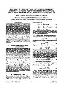
Table 1 shows the resulting uncertainty for different values of the current C·(dV/dt). For each uncertainty budget the main contribution is mentioned. For each measurement, 50 ramp sequences were taken, while every ramp period and every hold period consisted of 200 points. For currents of 10 fA and below, the absolute standard uncertainty is a few aA, fully determined by the type A evaluation. C. Calibration of a commercial picoammeter As a test of the use and reliability of the differentiating capacitor current source, we calibrated a commercial current meter with subfemtoampere resolution (Keithley 6430). For each sequence a positive and a negative current is determined. The measurement results are corrected for the zero offset of the meter, which is determined by averaging the second half of the values of the hold period before the ramp and the first half of the values of the hold period after the ramp (see Fig. 3), again skipping the first and last 10 to 30 points. Note that the zero offset of the current meter is measured during the hold period of the ramp generator, because also the ramp generator can have an offset. By zero correcting both the meter reading and the ramp rate we do not need to distinguish between the two offsets. Fig. 5 shows the result after this zero correction procedure for a calibration at a nominal value of 10 fA. Even though the offset, evaluated around –2 fA, varied by about ±0.5 fA the corrected value is stable within a standard deviation of ±100 aA. As in the case of the current source, the type A evaluation of the uncertainty for the measured current I is based on
the results per ramp as described in the previous section. The effect of varying the number of ramps and the number of points per ramp on the standard deviation of the mean turned out to be similar to that in the case of the evaluation of the current source. However, when repeating the experiment several times for the lowest currents, the standard deviation of the results of the different experiments is larger than the standard deviation of the mean for each individual experiment. This means that the long-term varying environmental conditions determine the overall uncertainty. Therefore, it does not make any sense to average over more ramps, and the best uncertainty that can be reported for such calibrations is determined by the standard deviation of the different experiments. The type B sources of uncertainty to be taken into account are: •
contribution from the source, see table 1;
•
effects from the input of the current meter: -
bias current (less than 3 fA), averaged out in the zero compensation procedure and contributing to the standard deviation
-
voltage burden (less than 1 mV) over the leak resistance, averaged out in the zero compensation procedure and contributing to the standard deviation
•
temperature coefficients of the gain resistors in the preamplifier of the current meter, which, according to specifications, is dependent on the range and varies from 2 fA/°C to 30 fA/°C; with the preamplifier temperature controlled within 0.1 °C this means 0.2 fA to 3 fA.
Table 2 shows the results for different values of the measured current I. For each uncertainty budget the main contribution is mentioned.
IV. CONCLUSIONS A high accuracy current source has been developed for the generation of very small currents (below 200 pA) based on applying a linear voltage ramp to a capacitor, with software-controlled compensation for the voltage ramp non-linearity. As compared to an analogue compensation network [2], our method has the significant additional
advantages of improved uncertainty, speed and flexibility. The deviation from linearity of the voltage ramp is measured and recorded, after which the necessary compensation is calculated in the software and applied in the next run. In principle this method can be used with any ramp rate or with any capacitor. The uncertainty is improved mainly because the effect of the leakage resistance of the capacitor, an important source of uncertainty, is symmetric with respect to zero volts across the capacitor and can be averaged out. In addition, the desired ramp rate can be reached within a few seconds. A voltage ramp within typically 10·10-6 of any desired value between less than 1 mV/s and several hundreds of mV/s can be realized. Using a high quality air-dielectric capacitor, currents below 200 pA can be generated with an uncertainty of 20 µA/A (k=2), with a lower limit of 2.0 aA (k=2). As a demonstration of the use and reliability of our current source, a commercial picoammeter has been calibrated down to a nominal value of 10 fA with an uncertainty of 230 aA. Environmental effects and the temperature coefficient of the feedback resistors in the preamplifier of the device under test limit the uncertainty. Other applications of our current source can be in single electron counting and single electron pumping experiments.
REFERENCES [1] G. Rietveld and H. Heimeriks, “Highly sensitive picoampere meter,” CPEM’96 Conf. Dig., 1996, pp. 332-333. [2] G.-D. Willenberg, H.N. Tauscher, and P. Warnecke, “A traceable precision current source for currents between 100 aA and 10 pA,” IEEE Trans. Instrum. Meas., vol. 52, pp. 436-439, 2002.
CAPTIONS
Table 1: Total uncertainties of the current C ·(dV/dt) generated using our set-up. For each measurement, 50 ramp sequences were taken, while every ramp or hold period consisted of 200 points.
Table 2: Total uncertainties for the calibration of a commercial picoammeter. Note that the preamplifier is temperature controlled within 0.1 °C in order to reduce the effect of the temperature coefficient (TC) of its gain resistors.
Fig. 1. Principle of the differentiating capacitor current source. A current I=Vin/R is converted to a voltage ramp by means of an opamp and a feedback capacitor C (the components in dashed lines represent its non-ideal behavior). The voltage ramp dV/dt is measured by a calibrated voltmeter and converted back into a current by an air-dielectric standard capacitor C’.
Fig. 2: Schematic set-up of the current source, with the voltage ramp circuit, digital voltmeter (DVM) and air-dielectric standard capacitor Cgas (see Fig. 1). Note that two voltage sources are used at the input, one of which is used for applying a correction signal to compensate for the voltage ramp non-linearity. The generated current can be applied to a picoammeter under test.
Fig. 3. Typical ramping sequence (hold, ramp up, hold, ramp down) that is repeated a number of times during a measurement. The software controlling the set-up allows the user to specify the number of sequences, the ramp rate, the ramp time and the hold time. The zero offset used for zero-correcting the current source and the picoammeter is determined by averaging the second half of the hold period before and the first half of the hold period after the ramp.
Fig. 4: Typical measurement of the ramp rate (in V/s) versus time (in s). The lower curve is recorded without compensation. Subsequent ramps are corrected by taking the remaining deviation from 0.1 V/s in the previous curve into account. The second curve is already very close to the desired value; the third curve (the upper one) is similar to the following curves.
Fig. 5: Calibration of a commercial picoammeter at 10 fA. Only the zero corrected values for the positive current readings are shown; the negative current readings shows similar behavior. Although the measured offset, of around -2 fA, varied by about ±0.5 fA during the measurements, the zero-corrected values are stable within a standard deviation of ±100 aA (which includes a small drift in the gain that can still be observed).
Nominal generated current
Expanded uncertainty (k=2)
Main contribution to the uncertainty
100 pA (1000 pF ⋅ 0.1 V/s)
2.0 fA
Capacitor
10 pA (100 pF ⋅ 0.1 V/s)
0.20 fA
Capacitor
1 pA (10 pF ⋅ 0.1 V/s)
20 aA
Capacitor
100 fA (10 pF ⋅ 0.01 V/s)
3.0 aA
Capacitor & Type A
10 fA (10 pF ⋅ 0.001 V/s)
2.0 aA
Type A
Nominal measured current
Expanded uncertainty (k=2)
Main contribution to the uncertainty
100 pA
4.0 fA
TC preamp
10 pA
1.4 fA
TC preamp
1 pA
0.4 fA
TC preamp
100 fA
0.25 fA
TC preamp
10 fA
0.23 fA
TC preamp
Vin
I C’
C R V
output voltage
hold
ramp up
hold
ramp down ramp rate
ramp rate hold time
ramp time
time hold time
ramp time
Ramp dV/dt (V/s)
0.10005
0.1
0.09995
0.0999
0.09985 0
50
100 Time (s)
150
200
Current (fA)
11.0 10.8 10.6 10.4 10.2 10.0 9.8 9.6 9.4 9.2 9.0 0
10
20
30
Ramp no.
40
50