ECOC 2009, 20-24 September, 2009, Vienna, Austria
Paper P2.27
All-Optical Spatial Multicasting Using Cascaded Silicon Photonic Devices Aleksandr Biberman(1), Noam Ophir(1), Benjamin G. Lee(1), Amy C. Turner-Foster(2), Mark A. Foster(3), Nicolás (2) (2) (2) (3) (1) Sherwood-Droz , Carl B. Poitras , Michal Lipson , Alexander L. Gaeta , Keren Bergman (1)
Department of Electrical Engineering, Columbia University, New York, NY, USA;
[email protected] School of Electrical and Computer Engineering, Cornell University, Ithaca, NY, USA (3) School of Applied and Engineering Physics, Cornell University, Ithaca, NY, USA (2)
Abstract We demonstrate all-optical spatial multicasting enabled by nanophotonic devices in two cascaded silicon chips. We evaluate each spatially-multicasted signal using 10-Gb/s BER measurements, facilitating the path towards fully-monolithic photonic integrated circuits performing complex network-level functionalities. Introduction Nonlinear optical processes such as four-wave mixing (FWM) enable ultrahigh-speed all-optical operations including broadband wavelength conversion, continuously tuneable delays, and signal regeneration1. Broadcasting and multicasting, critical network-level functionalities associated with selective dissemination of information, have traditionally been performed in the electronic domain using powerhungry optical-electronic-optical (O-E-O) conversions. Significant research on realizing all-optical FWMbased multicasting has been successful in fiberbased demonstrations2, which can be bulky and difficult to integrate with other network elements. Silicon, however, has enjoyed a long-standing role as the dominant material system in the microelectronics industry, and photonic devices that exploit the mature processing capabilities of the complementary metaloxide-semiconductor (CMOS) platform, including filters, switches, modulators, and detectors, are being demonstrated as well. Silicon’s large index of refraction allows dense photonic integration, making the prospects of complex photonic integrated circuits (PIC) and networks-on-chip (NoC) feasible3. The first demonstration of FWM-based on-chip multicasting in the silicon platform was recently reported4. This multicast circumvents the traditional power-demanding electronic domain, replacing it with the bandwidth-scalable, energy-efficient, and datarate-transparent optical domain, while remaining within the mass-producible silicon platform. The onchip multicasting was achieved in the wavelength domain by simultaneously converting many continuous-wave (CW) input channels into replicated A
A
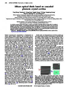
B
Fig. 1: Two silicon chips used to demonstrate spatial multicasting: (a) FWM chip achieves three-way wavelength multicast, and (b) ring resonator-based demultiplexer splits each wavelength channel into its respective output port.
data signals using a modulated pump signal. Here, we demonstrate the feasibility of spatial-domain onchip multicasting using silicon ring resonator-based filters to demultiplex three all-optically wavelengthmulticasted channels onto separate waveguides using two cascaded silicon chips. This demonstration is a key step in combining silicon nanophotonic building blocks, devices that are entirely amenable to single-chip dense integration, in order to achieve complex network-level functionalities. Cascaded Silicon Photonic Devices The devices discussed here (Fig. 1) were fabricated at the Cornell Nanofabrication Facility using electronbeam lithography followed by reactive-ion etching. The FWM device (chip 1, Fig. 1a) is a 1.1-cm-long waveguide with a height of 290 nm, slab thickness of 25 nm, and width of 680 nm. Previous work with a similar device showcased FWM-based wavelength conversion in silicon waveguides with larger than 150nm bandwidths using CW pumps1. We further demonstrated wavelength multicasting, with multicast number selectivity ranging from one-way to eight-way, B
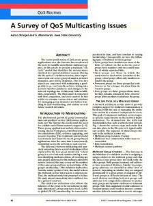
Fig. 2: (a) Diagram of experimental setup used for BER measurements. (b) 10-Gb/s eye diagrams recorded using the DCA for the input signal following the pump EDFA, as well as each output port of chip 2: through port, drop port 1, and drop port 2.
978-3-8007-3173-2 © VDE VERLAG GMBH
ECOC 2009, 20-24 September, 2009, Vienna, Austria
Paper P2.27
A
B
C
Fig. 3: Wavelength spectra for (a) resonance peaks of drop port 1 of chip 2, (b) resonance peaks of drop port 2 of chip 2, and (c) three-way 10-Gb/s wavelength multicasting observed at output of chip 1.
Fig. 4: BER curves recorded for each channel of a threeway spatially-multicasted signal at the through port (z), drop port 1 (▼), and drop port 2 (▲). Back-to-back curve () is taken for the pump signal following the pump EDFA.
and performed 40-Gb/s bit-error rate (BER) measurements4. The demultiplexer (chip 2, Fig. 1b) comprises a series of ring resonators with 20-µm diameters, each with a drop port guided toward the output of the chip. In this device, all of the waveguides have 250-nm heights and 450-nm widths.
First, wavelength multicasting is achieved on chip 1 by combining a modulated pump signal with three CW probes, producing three modulated output signals (Fig. 3c). The wavelengths of the output signals are respectively aligned so that two of the multicasted wavelength channels each correspond to a passband of a ring filter on chip 2 (Fig. 3a and Fig. 3b), and the third is off-resonance. Therefore, the three multicasted signals leave the device on three output ports: drop port 1, drop port 2, and through port. The spatial multicasting is achieved through the composite functionality of the two cascaded devices.
Spatial Multicasting Experiment The work presented here utilizes two chip-coupling setups, one for each silicon chip (Fig. 1), which employ tapered fibers to couple to on-chip nanotapered waveguides. The experimental setup for the BER measurements (Fig. 2a) incorporates three CW tunable laser (TL) sources acting as probes, and a fourth as the pump. The pump, operating at the 1552.4-nm wavelength, is externally modulated with a 10-Gb/s NRZ OOK signal, encoded using a PRBS of length 231-1, generated by the pulse pattern generator (PPG). The pump and probe signals are amplified using a C- and L-band erbium-doped fiber amplifier (EDFA), respectively, and then combined using a dense wavelength-division multiplexer (DWDM). The combined signals are then coupled into chip 1, which performs a three-way multicast of the original data signal. After exiting chip 1, the signals pass through a series of tunable grating filters (λ) and an EDFA, transmitting the three multicasted wavelength channels. The multicasted signals are subsequently coupled into chip 2. After exiting chip 2, the signals are filtered and amplified for evaluation, and pass through a variable optical attenuator (VOA) before being received by a high-speed p-i-n photodiode transimpedance amplifier (PIN-TIA) receiver followed by a limiting amplifier (LA). The signal is then analyzed using a BER tester (BERT). A fraction of the power is tapped-off after each chip for examination on an optical spectrum analyzer (OSA), and a digital communications analyzer (DCA) is used to obtain eye diagrams (Fig. 2b). Polarization controllers (PC) and fiber polarizers are also used throughout the setup.
978-3-8007-3173-2 © VDE VERLAG GMBH
Spatial Multicasting Results At each output port of chip 2, 10-Gb/s BER measurements are taken. Error-free operation (defined as having BERs less than 10-12) is observed at each output port, and a BER sensitivity curve is then taken for each case (Fig. 4). A back-to-back curve is recorded for the pump signal at the output of the pump amplifier, producing a 3.5-dB and 2.7-dB power penalty for the two drop ports and through port, respectively. For each configuration, an eye diagram is also obtained (Fig. 2b). Conclusions We demonstrate and evaluate all-optical spatial multicasting enabled by nanophotonic devices in two cascaded silicon chips. This work is a crucial step towards the goal of monolithic photonic integration with optically-transparent network-level functionalities enabling high-performance networks on- and off-chip. This work was supported in part by the DARPA MTO Parametric Optical Processes and Systems program under contract number W911NF-08-1-0058. References 1 M. A. Foster et al., Opt. Express, 15 12949 (2007). 2 C.-S. Brès et al., Proc. OFC’08, PDP16 (2008). 3 A. Shacham et al., Proc. HOTI’07 29 (2007). 4 A. Biberman et al., Proc. OFC’09, OTuI3 (2009).