Data Book Revision History . ...... Register Settings for Dither Enable/Disable
Feature . ...... tains a 1 in any of the other channel fields, the access goes.
AMD Geode™ LX Processors Data Book
February 2007 Publication ID: 33234E
AMD Geode™ LX Processors Data Book
© 2007 Advanced Micro Devices, Inc. All rights reserved. The contents of this document are provided in connection with Advanced Micro Devices, Inc. (“AMD”) products. AMD makes no representations or warranties with respect to the accuracy or completeness of the contents of this publication and reserves the right to make changes to specifications and product descriptions at any time without notice. No license, whether express, implied, arising by estoppel or otherwise, to any intellectual property rights is granted by this publication. Except as set forth in AMD’s Standard Terms and Conditions of Sale, AMD assumes no liability whatsoever, and disclaims any express or implied warranty, relating to its products including, but not limited to, the implied warranty of merchantability, fitness for a particular purpose, or infringement of any intellectual property right. AMD’s products are not designed, intended, authorized or warranted for use as components in systems intended for surgical implant into the body, or in other applications intended to support or sustain life, or in any other application in which the failure of AMD’s product could create a situation where personal injury, death, or severe property or environmental damage may occur. AMD reserves the right to discontinue or make changes to its products at any time without notice.
Contacts www.amd.com Trademarks AMD, the AMD Arrow logo, AMD Athlon, AMD Geode, and combinations thereof, and 3DNow! and GeodeLink, are trademarks of Advanced Micro Devices, Inc. AMD-K6 is a registered trademark of Advanced Micro Devices, Inc. Linux is a registered trademark of Linus Torvalds. WinBench is a registered trademark of Ziff Davis, Inc. Windows is a registered trademark of Microsoft Corporation in the United States and/or other jurisdictions. Pentium is a registered trademark and MMX is a trademark of Intel Corporation in the United States and/or other jurisdictions. Other product names used in this publication are for identification purposes only and may be trademarks of their respective companies.
2
AMD Geode™ LX Processors Data Book
Contents
33234E
Contents List of Figures . . . . . . . . . . . . . . . . . . . . . . . . . . . . . . . . . . . . . . . . . . . . . . . . . . . . . . . . . . 5 List of Tables . . . . . . . . . . . . . . . . . . . . . . . . . . . . . . . . . . . . . . . . . . . . . . . . . . . . . . . . . . . 7 1.0
Overview . . . . . . . . . . . . . . . . . . . . . . . . . . . . . . . . . . . . . . . . . . . . . . . . . . . . . . . . . 11 1.1 1.2
2.0
Architecture Overview . . . . . . . . . . . . . . . . . . . . . . . . . . . . . . . . . . . . . . . . . . . . . . 15 2.1 2.2 2.3 2.4 2.5 2.6 2.7 2.8 2.9 2.10
3.0
Buffer Types . . . . . . . . . . . . . . . . . . . . . . . . . . . . . . . . . . . . . . . . . . . . . . . . . . . . . . . . . . . . . . . . 23 Bootstrap Options . . . . . . . . . . . . . . . . . . . . . . . . . . . . . . . . . . . . . . . . . . . . . . . . . . . . . . . . . . . 24 Ball Assignments . . . . . . . . . . . . . . . . . . . . . . . . . . . . . . . . . . . . . . . . . . . . . . . . . . . . . . . . . . . . 24 Signal Descriptions . . . . . . . . . . . . . . . . . . . . . . . . . . . . . . . . . . . . . . . . . . . . . . . . . . . . . . . . . . 33
GeodeLink™ Interface Unit . . . . . . . . . . . . . . . . . . . . . . . . . . . . . . . . . . . . . . . . . . 45 4.1 4.2
5.0
CPU Core . . . . . . . . . . . . . . . . . . . . . . . . . . . . . . . . . . . . . . . . . . . . . . . . . . . . . . . . . . . . . . . . . 15 GeodeLink™ Control Processor . . . . . . . . . . . . . . . . . . . . . . . . . . . . . . . . . . . . . . . . . . . . . . . . 16 GeodeLink™ Interface Units . . . . . . . . . . . . . . . . . . . . . . . . . . . . . . . . . . . . . . . . . . . . . . . . . . . 16 GeodeLink™ Memory Controller . . . . . . . . . . . . . . . . . . . . . . . . . . . . . . . . . . . . . . . . . . . . . . . . 16 Graphics Processor . . . . . . . . . . . . . . . . . . . . . . . . . . . . . . . . . . . . . . . . . . . . . . . . . . . . . . . . . . 17 Display Controller . . . . . . . . . . . . . . . . . . . . . . . . . . . . . . . . . . . . . . . . . . . . . . . . . . . . . . . . . . . . 18 Video Processor . . . . . . . . . . . . . . . . . . . . . . . . . . . . . . . . . . . . . . . . . . . . . . . . . . . . . . . . . . . . 18 Video Input Port . . . . . . . . . . . . . . . . . . . . . . . . . . . . . . . . . . . . . . . . . . . . . . . . . . . . . . . . . . . . . 18 GeodeLink™ PCI Bridge . . . . . . . . . . . . . . . . . . . . . . . . . . . . . . . . . . . . . . . . . . . . . . . . . . . . . . 18 Security Block . . . . . . . . . . . . . . . . . . . . . . . . . . . . . . . . . . . . . . . . . . . . . . . . . . . . . . . . . . . . . . 19
Signal Definitions . . . . . . . . . . . . . . . . . . . . . . . . . . . . . . . . . . . . . . . . . . . . . . . . . . 21 3.1 3.2 3.3 3.4
4.0
General Description . . . . . . . . . . . . . . . . . . . . . . . . . . . . . . . . . . . . . . . . . . . . . . . . . . . . . . . . . . 11 Features . . . . . . . . . . . . . . . . . . . . . . . . . . . . . . . . . . . . . . . . . . . . . . . . . . . . . . . . . . . . . . . . . . . 12
MSR Set . . . . . . . . . . . . . . . . . . . . . . . . . . . . . . . . . . . . . . . . . . . . . . . . . . . . . . . . . . . . . . . . . . 45 GLIU Register Descriptions . . . . . . . . . . . . . . . . . . . . . . . . . . . . . . . . . . . . . . . . . . . . . . . . . . . . 50
CPU Core . . . . . . . . . . . . . . . . . . . . . . . . . . . . . . . . . . . . . . . . . . . . . . . . . . . . . . . . 89 5.1 5.2 5.3 5.4 5.5
Core Processor Initialization . . . . . . . . . . . . . . . . . . . . . . . . . . . . . . . . . . . . . . . . . . . . . . . . . . . 89 Instruction Set Overview . . . . . . . . . . . . . . . . . . . . . . . . . . . . . . . . . . . . . . . . . . . . . . . . . . . . . . 90 Application Register Set . . . . . . . . . . . . . . . . . . . . . . . . . . . . . . . . . . . . . . . . . . . . . . . . . . . . . . 91 System Register Set . . . . . . . . . . . . . . . . . . . . . . . . . . . . . . . . . . . . . . . . . . . . . . . . . . . . . . . . . 94 CPU Core Register Descriptions . . . . . . . . . . . . . . . . . . . . . . . . . . . . . . . . . . . . . . . . . . . . . . . . 99
AMD Geode™ LX Processors Data Book
3
33234E
6.0
Integrated Functions . . . . . . . . . . . . . . . . . . . . . . . . . . . . . . . . . . . . . . . . . . . . . . 209 6.1 6.2 6.3 6.4 6.5 6.6 6.7 6.8 6.9 6.10 6.11 6.12 6.13 6.14 6.15 6.16
7.0
Electrical Connections . . . . . . . . . . . . . . . . . . . . . . . . . . . . . . . . . . . . . . . . . . . . . . . . . . . . . . . 597 Absolute Maximum Ratings . . . . . . . . . . . . . . . . . . . . . . . . . . . . . . . . . . . . . . . . . . . . . . . . . . . 597 Operating Conditions . . . . . . . . . . . . . . . . . . . . . . . . . . . . . . . . . . . . . . . . . . . . . . . . . . . . . . . . 598 DC Current . . . . . . . . . . . . . . . . . . . . . . . . . . . . . . . . . . . . . . . . . . . . . . . . . . . . . . . . . . . . . . . . 599 DC Characteristics . . . . . . . . . . . . . . . . . . . . . . . . . . . . . . . . . . . . . . . . . . . . . . . . . . . . . . . . . . 603 AC Characteristics . . . . . . . . . . . . . . . . . . . . . . . . . . . . . . . . . . . . . . . . . . . . . . . . . . . . . . . . . . 606
Instruction Set . . . . . . . . . . . . . . . . . . . . . . . . . . . . . . . . . . . . . . . . . . . . . . . . . . . 617 8.1 8.2 8.3 8.4
9.0
GeodeLink™ Memory Controller . . . . . . . . . . . . . . . . . . . . . . . . . . . . . . . . . . . . . . . . . . . . . . . 210 GeodeLink™ Memory Controller Register Descriptions . . . . . . . . . . . . . . . . . . . . . . . . . . . . . 219 Graphics Processor . . . . . . . . . . . . . . . . . . . . . . . . . . . . . . . . . . . . . . . . . . . . . . . . . . . . . . . . . 237 Graphics Processor Register Definitions . . . . . . . . . . . . . . . . . . . . . . . . . . . . . . . . . . . . . . . . . 254 Display Controller . . . . . . . . . . . . . . . . . . . . . . . . . . . . . . . . . . . . . . . . . . . . . . . . . . . . . . . . . . . 278 Display Controller Register Descriptions . . . . . . . . . . . . . . . . . . . . . . . . . . . . . . . . . . . . . . . . . 300 Video Processor . . . . . . . . . . . . . . . . . . . . . . . . . . . . . . . . . . . . . . . . . . . . . . . . . . . . . . . . . . . 388 Video Processor Register Descriptions . . . . . . . . . . . . . . . . . . . . . . . . . . . . . . . . . . . . . . . . . . 412 Video Input Port . . . . . . . . . . . . . . . . . . . . . . . . . . . . . . . . . . . . . . . . . . . . . . . . . . . . . . . . . . . . 462 Video Input Port Register Descriptions . . . . . . . . . . . . . . . . . . . . . . . . . . . . . . . . . . . . . . . . . . 482 Security Block . . . . . . . . . . . . . . . . . . . . . . . . . . . . . . . . . . . . . . . . . . . . . . . . . . . . . . . . . . . . . 510 Security Block Register Descriptions . . . . . . . . . . . . . . . . . . . . . . . . . . . . . . . . . . . . . . . . . . . . 513 GeodeLink™ Control Processor . . . . . . . . . . . . . . . . . . . . . . . . . . . . . . . . . . . . . . . . . . . . . . . 533 GeodeLink™ Control Processor Register Descriptions . . . . . . . . . . . . . . . . . . . . . . . . . . . . . . 539 GeodeLink™ PCI Bridge . . . . . . . . . . . . . . . . . . . . . . . . . . . . . . . . . . . . . . . . . . . . . . . . . . . . . 566 GeodeLink™ PCI Bridge Register Descriptions . . . . . . . . . . . . . . . . . . . . . . . . . . . . . . . . . . . 572
Electrical Specifications . . . . . . . . . . . . . . . . . . . . . . . . . . . . . . . . . . . . . . . . . . . 597 7.1 7.2 7.3 7.4 7.5 7.6
8.0
General Instruction Set Format . . . . . . . . . . . . . . . . . . . . . . . . . . . . . . . . . . . . . . . . . . . . . . . . 617 CPUID Instruction Set . . . . . . . . . . . . . . . . . . . . . . . . . . . . . . . . . . . . . . . . . . . . . . . . . . . . . . . 625 Processor Core Instruction Set . . . . . . . . . . . . . . . . . . . . . . . . . . . . . . . . . . . . . . . . . . . . . . . . 631 MMX™, FPU, and AMD 3DNow!™ Technology Instructions Sets . . . . . . . . . . . . . . . . . . . . . . 656
Package Specifications . . . . . . . . . . . . . . . . . . . . . . . . . . . . . . . . . . . . . . . . . . . . 673 9.1
Physical Dimensions . . . . . . . . . . . . . . . . . . . . . . . . . . . . . . . . . . . . . . . . . . . . . . . . . . . . . . . . 673
Appendix A A.1 A.2
4
Contents
Support Documentation . . . . . . . . . . . . . . . . . . . . . . . . . . . . . . . . . . . . 675
Order Information . . . . . . . . . . . . . . . . . . . . . . . . . . . . . . . . . . . . . . . . . . . . . . . . . . . . . . . . . . 675 Data Book Revision History . . . . . . . . . . . . . . . . . . . . . . . . . . . . . . . . . . . . . . . . . . . . . . . . . . 677
AMD Geode™ LX Processors Data Book
List of Figures
33234E
List of Figures Figure 1-1. Figure 3-1. Figure 3-2. Figure 4-1. Figure 6-1. Figure 6-2. Figure 6-3. Figure 6-4. Figure 6-5. Figure 6-6. Figure 6-7. Figure 6-8. Figure 6-9. Figure 6-10. Figure 6-11. Figure 6-12. Figure 6-13. Figure 6-14. Figure 6-15. Figure 6-16. Figure 6-17. Figure 6-18. Figure 6-19. Figure 6-20. Figure 6-21. Figure 6-22. Figure 6-23. Figure 6-24. Figure 6-25. Figure 6-26. Figure 6-27. Figure 6-28. Figure 6-29. Figure 6-30. Figure 6-31. Figure 6-32. Figure 6-33. Figure 6-34. Figure 6-35. Figure 6-36. Figure 6-37. Figure 6-38. Figure 6-39. Figure 6-40. Figure 6-41.
Internal Block Diagram . . . . . . . . . . . . . . . . . . . . . . . . . . . . . . . . . . . . . . . . . . . . . . . . . . . . . . 11 Signal Groups . . . . . . . . . . . . . . . . . . . . . . . . . . . . . . . . . . . . . . . . . . . . . . . . . . . . . . . . . . . . 21 BGU481 Ball Assignment Diagram . . . . . . . . . . . . . . . . . . . . . . . . . . . . . . . . . . . . . . . . . . . . 25 GeodeLink™ Architecture . . . . . . . . . . . . . . . . . . . . . . . . . . . . . . . . . . . . . . . . . . . . . . . . . . . 46 Integrated Functions Block Diagram . . . . . . . . . . . . . . . . . . . . . . . . . . . . . . . . . . . . . . . . . . 209 GLMC Block Diagram . . . . . . . . . . . . . . . . . . . . . . . . . . . . . . . . . . . . . . . . . . . . . . . . . . . . . 210 HOI Addressing Example . . . . . . . . . . . . . . . . . . . . . . . . . . . . . . . . . . . . . . . . . . . . . . . . . . . 211 HOI Example . . . . . . . . . . . . . . . . . . . . . . . . . . . . . . . . . . . . . . . . . . . . . . . . . . . . . . . . . . . . 211 LOI Addressing Example . . . . . . . . . . . . . . . . . . . . . . . . . . . . . . . . . . . . . . . . . . . . . . . . . . . 212 LOI Example . . . . . . . . . . . . . . . . . . . . . . . . . . . . . . . . . . . . . . . . . . . . . . . . . . . . . . . . . . . . 212 Request Pipeline . . . . . . . . . . . . . . . . . . . . . . . . . . . . . . . . . . . . . . . . . . . . . . . . . . . . . . . . . 215 DDR Reads . . . . . . . . . . . . . . . . . . . . . . . . . . . . . . . . . . . . . . . . . . . . . . . . . . . . . . . . . . . . . 216 DDR Writes . . . . . . . . . . . . . . . . . . . . . . . . . . . . . . . . . . . . . . . . . . . . . . . . . . . . . . . . . . . . . 217 Graphics Processor Block Diagram . . . . . . . . . . . . . . . . . . . . . . . . . . . . . . . . . . . . . . . . . . . 237 14-Bit Repeated Pattern . . . . . . . . . . . . . . . . . . . . . . . . . . . . . . . . . . . . . . . . . . . . . . . . . . . 244 Display Controller High-Level Block Diagram . . . . . . . . . . . . . . . . . . . . . . . . . . . . . . . . . . . 278 GUI Block Diagram . . . . . . . . . . . . . . . . . . . . . . . . . . . . . . . . . . . . . . . . . . . . . . . . . . . . . . . 279 VGA Block Diagram . . . . . . . . . . . . . . . . . . . . . . . . . . . . . . . . . . . . . . . . . . . . . . . . . . . . . . . 280 VGA Frame Buffer Organization . . . . . . . . . . . . . . . . . . . . . . . . . . . . . . . . . . . . . . . . . . . . . 288 Graphics Controller High-level Diagram . . . . . . . . . . . . . . . . . . . . . . . . . . . . . . . . . . . . . . . 289 Write Mode Data Flow . . . . . . . . . . . . . . . . . . . . . . . . . . . . . . . . . . . . . . . . . . . . . . . . . . . . . 290 Read Mode Data Flow . . . . . . . . . . . . . . . . . . . . . . . . . . . . . . . . . . . . . . . . . . . . . . . . . . . . . 291 Color Compare Operation . . . . . . . . . . . . . . . . . . . . . . . . . . . . . . . . . . . . . . . . . . . . . . . . . . 292 Graphics Filter Block Diagram . . . . . . . . . . . . . . . . . . . . . . . . . . . . . . . . . . . . . . . . . . . . . . . 293 Flicker Filter and Line Buffer Path . . . . . . . . . . . . . . . . . . . . . . . . . . . . . . . . . . . . . . . . . . . . 295 Interlaced Timing Settings . . . . . . . . . . . . . . . . . . . . . . . . . . . . . . . . . . . . . . . . . . . . . . . . . . 298 Video Processor Block Diagram . . . . . . . . . . . . . . . . . . . . . . . . . . . . . . . . . . . . . . . . . . . . . 389 Video Processor Block Diagram . . . . . . . . . . . . . . . . . . . . . . . . . . . . . . . . . . . . . . . . . . . . . 390 Downscaler Block Diagram . . . . . . . . . . . . . . . . . . . . . . . . . . . . . . . . . . . . . . . . . . . . . . . . . 392 Linear Interpolation Calculation . . . . . . . . . . . . . . . . . . . . . . . . . . . . . . . . . . . . . . . . . . . . . . 393 Mixer Block Diagram . . . . . . . . . . . . . . . . . . . . . . . . . . . . . . . . . . . . . . . . . . . . . . . . . . . . . . 395 Color Key and Alpha-Blending Logic . . . . . . . . . . . . . . . . . . . . . . . . . . . . . . . . . . . . . . . . . . 396 VOP Internal Block Diagram . . . . . . . . . . . . . . . . . . . . . . . . . . . . . . . . . . . . . . . . . . . . . . . . 398 525-Line NTSC Video Window . . . . . . . . . . . . . . . . . . . . . . . . . . . . . . . . . . . . . . . . . . . . . . 399 HBLANK and VBLANK for Lines 20-262, 283-524 . . . . . . . . . . . . . . . . . . . . . . . . . . . . . . . 399 HBLANK and VBLANK for Lines 263, 525 . . . . . . . . . . . . . . . . . . . . . . . . . . . . . . . . . . . . . . 400 HBLANK and VBLANK for Lines 1-18, 264-281 . . . . . . . . . . . . . . . . . . . . . . . . . . . . . . . . . 400 HBLANK and VBLANK for Lines 19, 282 . . . . . . . . . . . . . . . . . . . . . . . . . . . . . . . . . . . . . . . 400 BT.656 8/16 Bit Line Data . . . . . . . . . . . . . . . . . . . . . . . . . . . . . . . . . . . . . . . . . . . . . . . . . . 403 Flat Panel Display Controller Block Diagram . . . . . . . . . . . . . . . . . . . . . . . . . . . . . . . . . . . . 405 Dithered 8x8 Pixel Pattern . . . . . . . . . . . . . . . . . . . . . . . . . . . . . . . . . . . . . . . . . . . . . . . . . . 408 N-Bit Dithering Pattern Schemes . . . . . . . . . . . . . . . . . . . . . . . . . . . . . . . . . . . . . . . . . . . . . 409 VIP Block Diagram . . . . . . . . . . . . . . . . . . . . . . . . . . . . . . . . . . . . . . . . . . . . . . . . . . . . . . . . 463 BT.656, 8/16-Bit Line Data . . . . . . . . . . . . . . . . . . . . . . . . . . . . . . . . . . . . . . . . . . . . . . . . . . 467 525 line, 60 Hz Digital Vertical Timing . . . . . . . . . . . . . . . . . . . . . . . . . . . . . . . . . . . . . . . . . 468
AMD Geode™ LX Processors Data Book
5
33234E
Figure 6-42. Figure 6-43. Figure 6-44. Figure 6-45. Figure 6-46. Figure 6-47. Figure 6-48. Figure 6-49. Figure 6-50. Figure 6-51. Figure 6-52. Figure 6-53. Figure 6-54. Figure 6-55. Figure 6-56. Figure 6-57. Figure 6-58. Figure 6-59. Figure 6-60. Figure 6-61. Figure 7-1. Figure 7-2. Figure 7-3. Figure 7-4. Figure 7-5. Figure 7-6. Figure 7-7. Figure 7-8. Figure 7-9. Figure 9-1. Figure 9-2. Figure A-1.
6
List of Figures
Ancillary Data Packets . . . . . . . . . . . . . . . . . . . . . . . . . . . . . . . . . . . . . . . . . . . . . . . . . . . . . 469 Message Passing Data Packet . . . . . . . . . . . . . . . . . . . . . . . . . . . . . . . . . . . . . . . . . . . . . . 470 Data Streaming Data Packet . . . . . . . . . . . . . . . . . . . . . . . . . . . . . . . . . . . . . . . . . . . . . . . . 470 BT.601 Mode Default Field Detection . . . . . . . . . . . . . . . . . . . . . . . . . . . . . . . . . . . . . . . . . 471 BT.601 Mode Programmable Field Detection . . . . . . . . . . . . . . . . . . . . . . . . . . . . . . . . . . . 472 BT.601 Mode Horizontal Timing . . . . . . . . . . . . . . . . . . . . . . . . . . . . . . . . . . . . . . . . . . . . . 472 BT.601 Mode Vertical Timing . . . . . . . . . . . . . . . . . . . . . . . . . . . . . . . . . . . . . . . . . . . . . . . . 473 YUV 4:2:2 to YUV 4:2:0 Translation . . . . . . . . . . . . . . . . . . . . . . . . . . . . . . . . . . . . . . . . . . 474 Dual Buffer for Message Passing and Data Streaming Modes . . . . . . . . . . . . . . . . . . . . . . 476 Example VIP YUV 4:2:2 SAV/EAV Packets Stored in System Memory in a Linear Buffer . 477 Example VIP YUV 4:2:0 Planar Buffer . . . . . . . . . . . . . . . . . . . . . . . . . . . . . . . . . . . . . . . . . 478 Example VIP 8/16- and 10-bit Ancillary Packets Stored in System Memory . . . . . . . . . . . . 479 Security Block Diagram . . . . . . . . . . . . . . . . . . . . . . . . . . . . . . . . . . . . . . . . . . . . . . . . . . . . 510 GLCP Block Diagram . . . . . . . . . . . . . . . . . . . . . . . . . . . . . . . . . . . . . . . . . . . . . . . . . . . . . . 533 Processor Clock Generation . . . . . . . . . . . . . . . . . . . . . . . . . . . . . . . . . . . . . . . . . . . . . . . . 536 GIO Interface Block Diagram . . . . . . . . . . . . . . . . . . . . . . . . . . . . . . . . . . . . . . . . . . . . . . . . 537 GLPCI Block Diagram . . . . . . . . . . . . . . . . . . . . . . . . . . . . . . . . . . . . . . . . . . . . . . . . . . . . . 566 Atomic MSR Accesses Across the PCI Bus . . . . . . . . . . . . . . . . . . . . . . . . . . . . . . . . . . . . 568 Simple Round-Robin . . . . . . . . . . . . . . . . . . . . . . . . . . . . . . . . . . . . . . . . . . . . . . . . . . . . . . 570 Weighted Round-Robin . . . . . . . . . . . . . . . . . . . . . . . . . . . . . . . . . . . . . . . . . . . . . . . . . . . . 570 VMEMLX Power Split . . . . . . . . . . . . . . . . . . . . . . . . . . . . . . . . . . . . . . . . . . . . . . . . . . . . . . 600 Drive Level and Measurement Points for Switching Characteristics . . . . . . . . . . . . . . . . . . 606 Drive Level and Measurement Points for Switching Characteristics . . . . . . . . . . . . . . . . . . 607 Power Up Sequencing . . . . . . . . . . . . . . . . . . . . . . . . . . . . . . . . . . . . . . . . . . . . . . . . . . . . . 608 Drive Level and Measurement Points for Switching Characteristics . . . . . . . . . . . . . . . . . . 608 Drive Level and Measurement Points for Switching Characteristics . . . . . . . . . . . . . . . . . . 609 Drive Level and Measurement Points for Switching Characteristics . . . . . . . . . . . . . . . . . . 610 DDR Write Timing Measurement Points . . . . . . . . . . . . . . . . . . . . . . . . . . . . . . . . . . . . . . . 614 DDR Read Timing Measurement Points . . . . . . . . . . . . . . . . . . . . . . . . . . . . . . . . . . . . . . . 615 BGU481 Top/Side View/Dimensions . . . . . . . . . . . . . . . . . . . . . . . . . . . . . . . . . . . . . . . . . . 673 BGU481 Bottom View/Dimensions . . . . . . . . . . . . . . . . . . . . . . . . . . . . . . . . . . . . . . . . . . . 674 AMD Geode™ LX Processors OPN Example . . . . . . . . . . . . . . . . . . . . . . . . . . . . . . . . . . . 675
AMD Geode™ LX Processors Data Book
List of Tables
33234E
List of Tables Table 2-1. Table 3-1. Table 3-2. Table 3-3. Table 3-4. Table 3-5. Table 3-6. Table 3-7. Table 4-1. Table 4-2. Table 4-3. Table 4-4. Table 4-5. Table 4-6. Table 4-7. Table 4-8. Table 4-9. Table 4-10. Table 5-1. Table 5-2. Table 5-3. Table 5-4. Table 5-5. Table 5-6. Table 5-7. Table 5-8. Table 5-9. Table 5-10. Table 5-11. Table 5-12. Table 5-13. Table 5-14. Table 5-15. Table 5-16. Table 5-17. Table 6-1. Table 6-2. Table 6-3. Table 6-4. Table 6-5. Table 6-6. Table 6-7. Table 6-8. Table 6-9. Table 6-10.
Graphics Processor Feature Comparison . . . . . . . . . . . . . . . . . . . . . . . . . . . . . . . . . . . . . . . 17 Video Signal Definitions Per Mode . . . . . . . . . . . . . . . . . . . . . . . . . . . . . . . . . . . . . . . . . . . . 22 Buffer Type Characteristics . . . . . . . . . . . . . . . . . . . . . . . . . . . . . . . . . . . . . . . . . . . . . . . . . . 23 Bootstrap Options . . . . . . . . . . . . . . . . . . . . . . . . . . . . . . . . . . . . . . . . . . . . . . . . . . . . . . . . . 24 Ball Type Definitions . . . . . . . . . . . . . . . . . . . . . . . . . . . . . . . . . . . . . . . . . . . . . . . . . . . . . . . 24 Ball Assignments - Sorted by Ball Number . . . . . . . . . . . . . . . . . . . . . . . . . . . . . . . . . . . . . . 26 Ball Assignments - Sorted Alphabetically by Signal Name . . . . . . . . . . . . . . . . . . . . . . . . . . 30 Signal Behavior During and After Reset . . . . . . . . . . . . . . . . . . . . . . . . . . . . . . . . . . . . . . . . 43 MSR Addressing . . . . . . . . . . . . . . . . . . . . . . . . . . . . . . . . . . . . . . . . . . . . . . . . . . . . . . . . . . 45 MSR Mapping . . . . . . . . . . . . . . . . . . . . . . . . . . . . . . . . . . . . . . . . . . . . . . . . . . . . . . . . . . . . 47 GLIU Memory Descriptor Address Hit and Routing Description . . . . . . . . . . . . . . . . . . . . . . 48 GLIU I/O Descriptor Address Hit and Routing Description . . . . . . . . . . . . . . . . . . . . . . . . . . 49 GeodeLink™ Device Standard MSRs Summary . . . . . . . . . . . . . . . . . . . . . . . . . . . . . . . . . . . . . . . . . . 50
GLIU Specific MSRs Summary . . . . . . . . . . . . . . . . . . . . . . . . . . . . . . . . . . . . . . . . . . . . . . . 50 GLIU Statistic and Comparator MSRs Summary . . . . . . . . . . . . . . . . . . . . . . . . . . . . . . . . . . 51 GLIU P2D Descriptor MSRs Summary . . . . . . . . . . . . . . . . . . . . . . . . . . . . . . . . . . . . . . . . . 53 GLIU Reserved MSRs Summary . . . . . . . . . . . . . . . . . . . . . . . . . . . . . . . . . . . . . . . . . . . . . . 53 GLIU IOD Descriptor MSRs Summary . . . . . . . . . . . . . . . . . . . . . . . . . . . . . . . . . . . . . . . . . . 54 Initialized Core Register Controls . . . . . . . . . . . . . . . . . . . . . . . . . . . . . . . . . . . . . . . . . . . . . 89 Application Register Set . . . . . . . . . . . . . . . . . . . . . . . . . . . . . . . . . . . . . . . . . . . . . . . . . . . . . 91 Segment Register Selection Rules . . . . . . . . . . . . . . . . . . . . . . . . . . . . . . . . . . . . . . . . . . . . 92 EFLAGS Register . . . . . . . . . . . . . . . . . . . . . . . . . . . . . . . . . . . . . . . . . . . . . . . . . . . . . . . . . 93 System Register Set . . . . . . . . . . . . . . . . . . . . . . . . . . . . . . . . . . . . . . . . . . . . . . . . . . . . . . . 94 Control Registers Map . . . . . . . . . . . . . . . . . . . . . . . . . . . . . . . . . . . . . . . . . . . . . . . . . . . . . . 95 CR4 Bit Descriptions . . . . . . . . . . . . . . . . . . . . . . . . . . . . . . . . . . . . . . . . . . . . . . . . . . . . . . . 96 CR3 Bit Descriptions . . . . . . . . . . . . . . . . . . . . . . . . . . . . . . . . . . . . . . . . . . . . . . . . . . . . . . . 96 CR2 Bit Descriptions . . . . . . . . . . . . . . . . . . . . . . . . . . . . . . . . . . . . . . . . . . . . . . . . . . . . . . . 96 CR0 Bit Descriptions . . . . . . . . . . . . . . . . . . . . . . . . . . . . . . . . . . . . . . . . . . . . . . . . . . . . . . . 96 Effects of Various Combinations of EM, TS, and MP Bits . . . . . . . . . . . . . . . . . . . . . . . . . . . 98 Standard GeodeLink™ Device MSRs Summary . . . . . . . . . . . . . . . . . . . . . . . . . . . . . . . . . . 99 CPU Core Specific MSRs Summary . . . . . . . . . . . . . . . . . . . . . . . . . . . . . . . . . . . . . . . . . . . 99 XC_HIST_MSR Exception Types . . . . . . . . . . . . . . . . . . . . . . . . . . . . . . . . . . . . . . . . . . . . 126 Region Properties Register Map . . . . . . . . . . . . . . . . . . . . . . . . . . . . . . . . . . . . . . . . . . . . . 170 Read Operations vs. Region Properties . . . . . . . . . . . . . . . . . . . . . . . . . . . . . . . . . . . . . . . 170 Write Operations vs. Region Properties . . . . . . . . . . . . . . . . . . . . . . . . . . . . . . . . . . . . . . . . 170 LOI - 2 DIMMs, Same Size, 1 DIMM Bank . . . . . . . . . . . . . . . . . . . . . . . . . . . . . . . . . . . . . 213 LOI - 2 DIMMs, Same Size, 2 DIMM Banks . . . . . . . . . . . . . . . . . . . . . . . . . . . . . . . . . . . . . 213 Non-Auto LOI - 1 or 2 DIMMs, Different Sizes, 1 DIMM Bank . . . . . . . . . . . . . . . . . . . . . . . 214 Non-Auto LOI - 1 or 2 DIMMs, Different Sizes, 2 DIMM Banks . . . . . . . . . . . . . . . . . . . . . . 214 Standard GeodeLink™ Device MSRs Summary . . . . . . . . . . . . . . . . . . . . . . . . . . . . . . . . . 219 GLMC Specific MSR Summary . . . . . . . . . . . . . . . . . . . . . . . . . . . . . . . . . . . . . . . . . . . . . . 219 Graphics Processor Feature Comparison . . . . . . . . . . . . . . . . . . . . . . . . . . . . . . . . . . . . . . 238 BLT Command Buffer Structure . . . . . . . . . . . . . . . . . . . . . . . . . . . . . . . . . . . . . . . . . . . . . . 239 Vector Command Buffer Structure . . . . . . . . . . . . . . . . . . . . . . . . . . . . . . . . . . . . . . . . . . . . 240 LUT (Lookup Table) Load Command Buffer Structure . . . . . . . . . . . . . . . . . . . . . . . . . . . . 240
AMD Geode™ LX Processors Data Book
7
33234E
Table 6-11. Table 6-12. Table 6-13. Table 6-14. Table 6-15. Table 6-16. Table 6-17. Table 6-18. Table 6-19. Table 6-20. Table 6-21. Table 6-22. Table 6-23. Table 6-24. Table 6-25. Table 6-26. Table 6-27. Table 6-28. Table 6-29. Table 6-30. Table 6-31. Table 6-32. Table 6-33. Table 6-34. Table 6-35. Table 6-36. Table 6-37. Table 6-38. Table 6-39. Table 6-40. Table 6-41. Table 6-42. Table 6-43. Table 6-44. Table 6-45. Table 6-46. Table 6-47. Table 6-48. Table 6-49. Table 6-50. Table 6-51. Table 6-52. Table 6-53. Table 6-54. Table 6-55. Table 6-56. Table 6-57. Table 6-58. Table 6-59. Table 6-60. Table 6-61. Table 6-62. Table 6-63. Table 6-64. Table 6-65.
8
List of Tables
Data Only Command Buffer Structure . . . . . . . . . . . . . . . . . . . . . . . . . . . . . . . . . . . . . . . . . 240 Bit Descriptions . . . . . . . . . . . . . . . . . . . . . . . . . . . . . . . . . . . . . . . . . . . . . . . . . . . . . . . . . . 241 Pixel Ordering for 4-Bit Pixels . . . . . . . . . . . . . . . . . . . . . . . . . . . . . . . . . . . . . . . . . . . . . . . 243 Example Vector Pattern . . . . . . . . . . . . . . . . . . . . . . . . . . . . . . . . . . . . . . . . . . . . . . . . . . . . 244 Example Vector Length . . . . . . . . . . . . . . . . . . . . . . . . . . . . . . . . . . . . . . . . . . . . . . . . . . . . 244 Example of Monochrome Pattern . . . . . . . . . . . . . . . . . . . . . . . . . . . . . . . . . . . . . . . . . . . . 247 Example of 8-Bit Color Pattern (3:3:2 Format) . . . . . . . . . . . . . . . . . . . . . . . . . . . . . . . . . . . 248 Example of 16-Bit Color Pattern (5:6:5 Format) . . . . . . . . . . . . . . . . . . . . . . . . . . . . . . . . . . 248 32-bpp 8:8:8:8 Color Data Format . . . . . . . . . . . . . . . . . . . . . . . . . . . . . . . . . . . . . . . . . . . . 249 16-bpp Color Data Format . . . . . . . . . . . . . . . . . . . . . . . . . . . . . . . . . . . . . . . . . . . . . . . . . . 249 8-bpp 3:3:2 Color Data Format . . . . . . . . . . . . . . . . . . . . . . . . . . . . . . . . . . . . . . . . . . . . . . 249 Monochrome Data Format . . . . . . . . . . . . . . . . . . . . . . . . . . . . . . . . . . . . . . . . . . . . . . . . . . 249 Example of Byte-Packed Monochrome Source Data . . . . . . . . . . . . . . . . . . . . . . . . . . . . . . 250 Example of Unpacked Monochrome Source Data . . . . . . . . . . . . . . . . . . . . . . . . . . . . . . . . 250 GP_RASTER_MODE Bit Patterns . . . . . . . . . . . . . . . . . . . . . . . . . . . . . . . . . . . . . . . . . . . . 251 Common Raster Operations . . . . . . . . . . . . . . . . . . . . . . . . . . . . . . . . . . . . . . . . . . . . . . . . 251 Alpha Blending Modes . . . . . . . . . . . . . . . . . . . . . . . . . . . . . . . . . . . . . . . . . . . . . . . . . . . . . 252 Standard GeodeLink™ Device MSRs Summary . . . . . . . . . . . . . . . . . . . . . . . . . . . . . . . . . 254 Graphics Processor Configuration Register Summary . . . . . . . . . . . . . . . . . . . . . . . . . . . . 254 PAT_COLOR Usage for Color Patterns . . . . . . . . . . . . . . . . . . . . . . . . . . . . . . . . . . . . . . . . 264 PAT_DATA Usage for Color Patterns . . . . . . . . . . . . . . . . . . . . . . . . . . . . . . . . . . . . . . . . . 265 Display Modes . . . . . . . . . . . . . . . . . . . . . . . . . . . . . . . . . . . . . . . . . . . . . . . . . . . . . . . . . . . 281 Cursor Display Encodings . . . . . . . . . . . . . . . . . . . . . . . . . . . . . . . . . . . . . . . . . . . . . . . . . . 283 Icon Display Encodings . . . . . . . . . . . . . . . . . . . . . . . . . . . . . . . . . . . . . . . . . . . . . . . . . . . . 283 Cursor/Color Key/Alpha Interaction . . . . . . . . . . . . . . . . . . . . . . . . . . . . . . . . . . . . . . . . . . . 284 Video Bandwidth . . . . . . . . . . . . . . . . . . . . . . . . . . . . . . . . . . . . . . . . . . . . . . . . . . . . . . . . . 286 YUV 4:2:0 Video Data Ordering . . . . . . . . . . . . . . . . . . . . . . . . . . . . . . . . . . . . . . . . . . . . . . 287 YUV 4:2:2 Video Data Ordering . . . . . . . . . . . . . . . . . . . . . . . . . . . . . . . . . . . . . . . . . . . . . . 287 VGA Text Modes . . . . . . . . . . . . . . . . . . . . . . . . . . . . . . . . . . . . . . . . . . . . . . . . . . . . . . . . . 288 Text Mode Attribute Byte Format . . . . . . . . . . . . . . . . . . . . . . . . . . . . . . . . . . . . . . . . . . . . . 288 VGA Graphics Modes . . . . . . . . . . . . . . . . . . . . . . . . . . . . . . . . . . . . . . . . . . . . . . . . . . . . . 288 Programming Image Sizes . . . . . . . . . . . . . . . . . . . . . . . . . . . . . . . . . . . . . . . . . . . . . . . . . . 297 Vertical Timing in Number of Lines . . . . . . . . . . . . . . . . . . . . . . . . . . . . . . . . . . . . . . . . . . . 298 Timing Register Settings for Interlaced Modes . . . . . . . . . . . . . . . . . . . . . . . . . . . . . . . . . . 299 Standard GeodeLink™ Device MSRs Summary . . . . . . . . . . . . . . . . . . . . . . . . . . . . . . . . . 300 DC Specific MSRs Summary . . . . . . . . . . . . . . . . . . . . . . . . . . . . . . . . . . . . . . . . . . . . . . . . 300 DC Configuration Control Register Summary . . . . . . . . . . . . . . . . . . . . . . . . . . . . . . . . . . . 300 VGA Block Configuration Register Summary . . . . . . . . . . . . . . . . . . . . . . . . . . . . . . . . . . . 303 VGA Block Standard Register Summary . . . . . . . . . . . . . . . . . . . . . . . . . . . . . . . . . . . . . . . 303 VGA Block Extended Register Summary . . . . . . . . . . . . . . . . . . . . . . . . . . . . . . . . . . . . . . . 304 VGA Sequencer Registers Summary . . . . . . . . . . . . . . . . . . . . . . . . . . . . . . . . . . . . . . . . . 358 Font Table . . . . . . . . . . . . . . . . . . . . . . . . . . . . . . . . . . . . . . . . . . . . . . . . . . . . . . . . . . . . . . 360 CRTC Register Settings . . . . . . . . . . . . . . . . . . . . . . . . . . . . . . . . . . . . . . . . . . . . . . . . . . . . 361 CRTC Registers Summary . . . . . . . . . . . . . . . . . . . . . . . . . . . . . . . . . . . . . . . . . . . . . . . . . 362 CRTC Memory Addressing Modes . . . . . . . . . . . . . . . . . . . . . . . . . . . . . . . . . . . . . . . . . . . 371 Graphics Controller Registers Summary . . . . . . . . . . . . . . . . . . . . . . . . . . . . . . . . . . . . . . . 373 Attribute Controller Registers Summary . . . . . . . . . . . . . . . . . . . . . . . . . . . . . . . . . . . . . . . 378 Video DAC Registers Summary . . . . . . . . . . . . . . . . . . . . . . . . . . . . . . . . . . . . . . . . . . . . . . 382 Extended Registers Summary . . . . . . . . . . . . . . . . . . . . . . . . . . . . . . . . . . . . . . . . . . . . . . . 384 Truth Table for Alpha-Blending . . . . . . . . . . . . . . . . . . . . . . . . . . . . . . . . . . . . . . . . . . . . . . 397 VOP Mode . . . . . . . . . . . . . . . . . . . . . . . . . . . . . . . . . . . . . . . . . . . . . . . . . . . . . . . . . . . . . . 401 SAV/EAV Sequence . . . . . . . . . . . . . . . . . . . . . . . . . . . . . . . . . . . . . . . . . . . . . . . . . . . . . . 402 Protection Bit Values . . . . . . . . . . . . . . . . . . . . . . . . . . . . . . . . . . . . . . . . . . . . . . . . . . . . . . 402 SAV VIP Flags . . . . . . . . . . . . . . . . . . . . . . . . . . . . . . . . . . . . . . . . . . . . . . . . . . . . . . . . . . . 404 VOP Clock Rate . . . . . . . . . . . . . . . . . . . . . . . . . . . . . . . . . . . . . . . . . . . . . . . . . . . . . . . . . . 404
AMD Geode™ LX Processors Data Book -
33234E
List of Tables
Table 6-66. Table 6-67. Table 6-68. Table 6-69. Table 6-70. Table 6-71. Table 6-72. Table 6-73. Table 6-74. Table 6-75. Table 6-76. Table 6-77. Table 6-78. Table 6-79. Table 6-80. Table 6-81. Table 6-82. Table 6-83. Table 6-84. Table 6-85. Table 6-86. Table 6-87. Table 6-88. Table 6-89. Table 6-90. Table 6-91. Table 6-92. Table 6-93. Table 7-1. Table 7-2. Table 7-3. Table 7-4. Table 7-5. Table 7-6. Table 7-7. Table 7-8. Table 7-9. Table 7-10. Table 7-11. Table 7-12. Table 7-13. Table 7-14. Table 7-15. Table 8-1. Table 8-2. Table 8-3. Table 8-4. Table 8-5. Table 8-6. Table 8-7. Table 8-8. Table 8-9. Table 8-10. Table 8-11. Table 8-12.
Panel Output Signal Mapping . . . . . . . . . . . . . . . . . . . . . . . . . . . . . . . . . . . . . . . . . . . . . . . 406 Register Settings for Dither Enable/Disable Feature . . . . . . . . . . . . . . . . . . . . . . . . . . . . . . 410 Display RGB Modes . . . . . . . . . . . . . . . . . . . . . . . . . . . . . . . . . . . . . . . . . . . . . . . . . . . . . . . 411 Standard GeodeLink™ Device MSRs Summary . . . . . . . . . . . . . . . . . . . . . . . . . . . . . . . . . 412 Video Processor Module Specific MSRs Summary . . . . . . . . . . . . . . . . . . . . . . . . . . . . . . . 412 Video Processor Module Configuration Control Registers Summary . . . . . . . . . . . . . . . . . 412 VIP Capabilities . . . . . . . . . . . . . . . . . . . . . . . . . . . . . . . . . . . . . . . . . . . . . . . . . . . . . . . . . . 462 SAV/EAV Sequence . . . . . . . . . . . . . . . . . . . . . . . . . . . . . . . . . . . . . . . . . . . . . . . . . . . . . . 466 VIP Data Types / Memory Registers . . . . . . . . . . . . . . . . . . . . . . . . . . . . . . . . . . . . . . . . . . 475 Standard GeodeLink™ Device MSRs Summary . . . . . . . . . . . . . . . . . . . . . . . . . . . . . . . . . 482 VIP Configuration/Control Registers Summary . . . . . . . . . . . . . . . . . . . . . . . . . . . . . . . . . . 482 EEPROM Address Map . . . . . . . . . . . . . . . . . . . . . . . . . . . . . . . . . . . . . . . . . . . . . . . . . . . . 512 Standard GeodeLink™ Device MSRs Summary . . . . . . . . . . . . . . . . . . . . . . . . . . . . . . . . . 513 Security Block Specific MSRs . . . . . . . . . . . . . . . . . . . . . . . . . . . . . . . . . . . . . . . . . . . . . . . 513 Security Block Configuration/Control Registers Summary . . . . . . . . . . . . . . . . . . . . . . . . . . 513 TAP Control Instructions (25-Bit IR) . . . . . . . . . . . . . . . . . . . . . . . . . . . . . . . . . . . . . . . . . . . 534 TAP Instruction Bits . . . . . . . . . . . . . . . . . . . . . . . . . . . . . . . . . . . . . . . . . . . . . . . . . . . . . . . 534 GIO_PCI Outputs . . . . . . . . . . . . . . . . . . . . . . . . . . . . . . . . . . . . . . . . . . . . . . . . . . . . . . . . . 537 CIS Signaling Protocol . . . . . . . . . . . . . . . . . . . . . . . . . . . . . . . . . . . . . . . . . . . . . . . . . . . . . 538 Standard GeodeLink™ Device MSRs Summary . . . . . . . . . . . . . . . . . . . . . . . . . . . . . . . . . 539 GLCP Specific MSRs Summary . . . . . . . . . . . . . . . . . . . . . . . . . . . . . . . . . . . . . . . . . . . . . 539 Bootstrap Bit Settings and Reset State of GLCP_SYS_RSTPLL (PW1 and IRQ13 = 0) . . 556 Bootstrap Bit Settings and Reset State of GLCP_SYS_RSTPLL (PW1 and IRQ13 vary) . . 557 Format for Accessing the Internal PCI Configuration Registers . . . . . . . . . . . . . . . . . . . . . 569 PCI Device to AD Bus Mapping . . . . . . . . . . . . . . . . . . . . . . . . . . . . . . . . . . . . . . . . . . . . . . 570 Standard GeodeLink™ Device MSRs Summary . . . . . . . . . . . . . . . . . . . . . . . . . . . . . . . . . 572 GLPCI Specific Registers Summary . . . . . . . . . . . . . . . . . . . . . . . . . . . . . . . . . . . . . . . . . . 572 Region Properties . . . . . . . . . . . . . . . . . . . . . . . . . . . . . . . . . . . . . . . . . . . . . . . . . . . . . . . . 586 Absolute Maximum Ratings . . . . . . . . . . . . . . . . . . . . . . . . . . . . . . . . . . . . . . . . . . . . . . . . . 597 Operating Conditions . . . . . . . . . . . . . . . . . . . . . . . . . . . . . . . . . . . . . . . . . . . . . . . . . . . . . . 598 AMD Geode LX
[email protected] Processor DC Currents . . . . . . . . . . . . . . . . . . . . . . . . . . . . . 600 AMD Geode LX
[email protected] Processor DC Currents . . . . . . . . . . . . . . . . . . . . . . . . . . . . . 601 AMD Geode LX
[email protected] Processor DC Currents . . . . . . . . . . . . . . . . . . . . . . . . . . . . . 602 DC Characteristics . . . . . . . . . . . . . . . . . . . . . . . . . . . . . . . . . . . . . . . . . . . . . . . . . . . . . . . 603 System Interface Signals . . . . . . . . . . . . . . . . . . . . . . . . . . . . . . . . . . . . . . . . . . . . . . . . . . . 607 PCI Interface Signals . . . . . . . . . . . . . . . . . . . . . . . . . . . . . . . . . . . . . . . . . . . . . . . . . . . . . . 608 VIP Interface Signals . . . . . . . . . . . . . . . . . . . . . . . . . . . . . . . . . . . . . . . . . . . . . . . . . . . . . . 609 Flat Panel Interface Signals . . . . . . . . . . . . . . . . . . . . . . . . . . . . . . . . . . . . . . . . . . . . . . . . . 610 CRT Interface Signals . . . . . . . . . . . . . . . . . . . . . . . . . . . . . . . . . . . . . . . . . . . . . . . . . . . . . 611 CRT Display Recommended Operating Conditions . . . . . . . . . . . . . . . . . . . . . . . . . . . . . . . 611 CRT Display Analog (DAC) Characteristics . . . . . . . . . . . . . . . . . . . . . . . . . . . . . . . . . . . . . 612 Memory (DDR) Interface Signals . . . . . . . . . . . . . . . . . . . . . . . . . . . . . . . . . . . . . . . . . . . . . 613 JTAG Interface Signals . . . . . . . . . . . . . . . . . . . . . . . . . . . . . . . . . . . . . . . . . . . . . . . . . . . . 616 General Instruction Set Format . . . . . . . . . . . . . . . . . . . . . . . . . . . . . . . . . . . . . . . . . . . . . . 617 Instruction Fields . . . . . . . . . . . . . . . . . . . . . . . . . . . . . . . . . . . . . . . . . . . . . . . . . . . . . . . . . 618 Instruction Prefix Summary . . . . . . . . . . . . . . . . . . . . . . . . . . . . . . . . . . . . . . . . . . . . . . . . . 618 w Field Encoding . . . . . . . . . . . . . . . . . . . . . . . . . . . . . . . . . . . . . . . . . . . . . . . . . . . . . . . . . 619 d Field Encoding . . . . . . . . . . . . . . . . . . . . . . . . . . . . . . . . . . . . . . . . . . . . . . . . . . . . . . . . . 619 s Field Encoding . . . . . . . . . . . . . . . . . . . . . . . . . . . . . . . . . . . . . . . . . . . . . . . . . . . . . . . . . 619 eee Field Encoding . . . . . . . . . . . . . . . . . . . . . . . . . . . . . . . . . . . . . . . . . . . . . . . . . . . . . . . 620 mod r/m Field Encoding . . . . . . . . . . . . . . . . . . . . . . . . . . . . . . . . . . . . . . . . . . . . . . . . . . . . 620 General Registers Selected by mod r/m Fields and w Field . . . . . . . . . . . . . . . . . . . . . . . . 621 reg Field . . . . . . . . . . . . . . . . . . . . . . . . . . . . . . . . . . . . . . . . . . . . . . . . . . . . . . . . . . . . . . . . 622 sreg2 Field Encoding . . . . . . . . . . . . . . . . . . . . . . . . . . . . . . . . . . . . . . . . . . . . . . . . . . . . . . 622 sreg3 Field (FS and GS Segment Register Selection) . . . . . . . . . . . . . . . . . . . . . . . . . . . . 622
AMD Geode™ LX Processors Data Book
9
33234E
Table 8-13. Table 8-14. Table 8-15. Table 8-16. Table 8-17. Table 8-18. Table 8-19. Table 8-20. Table 8-21. Table 8-22. Table 8-23. Table 8-24. Table 8-25. Table 8-26. Table 8-27. Table 8-28. Table 8-29. Table 8-30. Table A-1. Table A-2. Table A-3.
10
List of Tables
ss Field Encoding . . . . . . . . . . . . . . . . . . . . . . . . . . . . . . . . . . . . . . . . . . . . . . . . . . . . . . . . . 623 index Field Encoding . . . . . . . . . . . . . . . . . . . . . . . . . . . . . . . . . . . . . . . . . . . . . . . . . . . . . . 623 mod base Field Encoding . . . . . . . . . . . . . . . . . . . . . . . . . . . . . . . . . . . . . . . . . . . . . . . . . . 624 CPUID Instruction with EAX = 00000000h . . . . . . . . . . . . . . . . . . . . . . . . . . . . . . . . . . . . . 625 CPUID Instruction with EAX = 00000001h . . . . . . . . . . . . . . . . . . . . . . . . . . . . . . . . . . . . . 625 CPUID Instruction Codes with EAX = 00000000 . . . . . . . . . . . . . . . . . . . . . . . . . . . . . . . . . 626 CPUID Instruction with EAX = 80000000h . . . . . . . . . . . . . . . . . . . . . . . . . . . . . . . . . . . . . 627 CPUID Instruction with EAX = 80000001h . . . . . . . . . . . . . . . . . . . . . . . . . . . . . . . . . . . . . 627 CPUID Instruction Codes with EAX = 80000001h . . . . . . . . . . . . . . . . . . . . . . . . . . . . . . . . 628 CPUID Instruction with EAX = 80000002h, 80000003h, or 80000004h . . . . . . . . . . . . . . . 629 CPUID Instruction with EAX = 80000005h . . . . . . . . . . . . . . . . . . . . . . . . . . . . . . . . . . . . . 630 CPUID Instruction with EAX = 80000006h . . . . . . . . . . . . . . . . . . . . . . . . . . . . . . . . . . . . . 630 Processor Core Instruction Set Table Legend . . . . . . . . . . . . . . . . . . . . . . . . . . . . . . . . . . . 631 Processor Core Instruction Set . . . . . . . . . . . . . . . . . . . . . . . . . . . . . . . . . . . . . . . . . . . . . . 632 MMX™, FPU, and AMD 3DNow!™ Instruction Set Table Legend . . . . . . . . . . . . . . . . . . . 656 MMX™ Instruction Set . . . . . . . . . . . . . . . . . . . . . . . . . . . . . . . . . . . . . . . . . . . . . . . . . . . . . 658 FPU Instruction Set . . . . . . . . . . . . . . . . . . . . . . . . . . . . . . . . . . . . . . . . . . . . . . . . . . . . . . . 665 AMD 3DNow!™ Technology Instruction Set . . . . . . . . . . . . . . . . . . . . . . . . . . . . . . . . . . . . 669 Valid OPN Combinations . . . . . . . . . . . . . . . . . . . . . . . . . . . . . . . . . . . . . . . . . . . . . . . . . . . 676 Revision History . . . . . . . . . . . . . . . . . . . . . . . . . . . . . . . . . . . . . . . . . . . . . . . . . . . . . . . . . . 677 Edits to Current Revision . . . . . . . . . . . . . . . . . . . . . . . . . . . . . . . . . . . . . . . . . . . . . . . . . . . 677
AMD Geode™ LX Processors Data Book -
Overview
33234E
1
1.0Overview 1.1
General Description
AMD Geode™ LX processors are integrated x86 processors specifically designed to power embedded devices for entertainment, education, and business. Serving the needs of consumers and business professionals alike, it’s an excellent solution for embedded applications, such as thin clients, interactive set-top boxes, single board computers, and mobile computing devices. Available with a core voltage of 1.2V, it offers extremely low typical power consumption leading to longer battery life and enabling small form-factor, fanless designs. SYSREF
Clock Module System PLL
DOTREF
CPU PLL DOTCLK PLL
While the processor core provides maximum compatibility with the vast amount of Internet content available, the intelligent integration of several other functions, including graphics and video datapaths, offers a true system-level multimedia solution. For implementation details and suggestions for this device, see the supporting documentation (i.e., application notes, schematics, etc.) on the AMD Embedded Developer Support Web site (NDA required - http://www.amd.com/embedded/developer).. CPU Core
64 KB L1 I-cache 64 KB L1 D-cache TLB
Integer Unit
Graphics Processor (GP) BLT Engine
MMU Load/Store
FPU ROP Unit
Bus Controller
Alpha Compositing
128 KB L2 cache
SDCLKs
64-Bit DDR
Test/Reset Interface
GeodeLink™ Memory Controller (GLMC)
Rotation BLT
GeodeLink™ Interface Unit 0 (GLIU0)
64-bit DDR SDRAM
GeodeLink™ Control Processor (GLCP)
Display Controller (DC) Compression Buffer
GeodeLink™ Interface Unit 1 (GLIU1)
Palette RAM Timing
Power Mgmnt
Graphics Filter/Scaling
Test
HW VGA
Diagnostic
AMD Geode™ Companion Device
Companion I/F
RGB
YUV
Video Processor (VP)
Security Block 128-bit AES (CBC/ECB)
1 KB LUT
Video Input Port (VIP)
GeodeLink™ PCI Bridge (GLPCI)
True Random Number Generator
TFT Controller/ Video Output Port (VOP)
Video Scalar Video Mixer Alpha Blender
3x8-Bit DAC EEPROM on package (optional)
VIP
PCI
TFT/VOP CRT
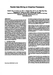
Figure 1-1. Internal Block Diagram
AMD Geode™ LX Processors Data Book
11
33234E
1.2
Overview
Features
General Features ■ Functional blocks include:
— — — — — — —
CPU Core GeodeLink™ Control Processor GeodeLink Interface Units GeodeLink Memory Controller Graphics Processor Display Controller Video Processor – TFT Controller/Video Output Port — Video Input Port — GeodeLink PCI Bridge — Security Block ■ 0.13 micron process ■ Packaging:
— 481-Terminal BGU (Ball Grid Array Cavity Up) with internal heatspreader
■ Power Management:
— LX
[email protected] processor* (Unterminated): Total Dissipated Power (TDP) 5.1W, 2.6W typical @ 500 MHz max power — LX
[email protected] processor* (Unterminated): Total Dissipated Power (TDP) 3.6W, 1.8W typical @ 500 MHz max power — LX
[email protected] processor* (Unterminated): Total Dissipated Power (TDP) 3.1W, 1.3W typical @ 500 MHz max power — GeodeLink active hardware power management — Hardware support for standard ACPI software power management — I/O companion SUSP/SUSPA power controls — Lower power I/O — Wakeup on SMI/INTR ■ Works in conjunction with the AMD Geode™ CS5536
(USB 2.0) or CS5535 (USB 1.1) companion device
■ Single packaging option supports all features
GeodeLink™ Architecture
CPU Processor Features
■ High bandwidth packetized uni-directional bus for
■ x86/x87-compatible CPU core ■ Performance:
— Processor frequency: up to 600 MHz — Dhrystone 2.1 MIPs: 150 to 450 — Fully pipelined FPU ■ Split I/D cache/TLB (Translation Look-aside Buffer):
— 64 KB I-cache/64 KB D-cache — 128 KB L2 cache configurable as I-cache, D-cache, or both ■ Efficient prefetch and branch prediction ■ Integrated FPU that supports the MMX™ and
AMD 3DNow!™ instruction sets ■ Fully pipelined single precision FPU hardware with
microcode support for higher precisions
internal peripherals ■ Standardized protocol to allow variants of products to be
developed by adding or removing modules ■ GeodeLink Control Processor (GLCP) for diagnostics
and scan control ■ Dual GeodeLink Interface Units (GLIUs) for device inter-
connect GeodeLink™ Memory Controller ■ Integrated memory controller for low latency to CPU and
on-chip peripherals ■ 64-bit wide DDR SDRAM bus operating frequency:
— 200 MHz, 400 MT/S ■ Supports unbuffered DDR DIMMS using up to 1 GB
DRAM technology GeodeLink™ Control Processor ■ JTAG interface:
— ATPG, Full Scan, BIST on all arrays — 1149.1 Boundary Scan compliant
■ Supports up to 2 DIMMS (16 devices max)
2D Graphics Processor ■ High performance 2D graphics controller
■ ICE (in-circuit emulator) interface
■ Alpha BLT
■ Reset and clock control
■ Windows® GDI GUI acceleration:
■ Designed for improved software debug methods and
performance analysis
— Hardware support for all Microsoft RDP codes ■ Command buffer interface for asynchronous BLTs ■ Second pattern channel support ■ Hardware screen rotation
*The AMD Geode LX
[email protected] processor operates at 600 MHz, the AMD Geode LX
[email protected] processor operates at 500 MHz, and the AMD Geode LX
[email protected] processor operates at 433 MHz. Model numbers reflect performance as described here: http://www.amd.com/connectivitysolutions/geodelxbenchmark. 12
AMD Geode™ LX Processors Data Book
33234E
Overview
Display Controller
GeodeLink™ PCI Bridge
■ Hardware frame buffer compression improves Unified
■ PCI 2.2 compliant
Memory Architecture (UMA) memory efficiency ■ CRT resolutions supported:
— Supports up to 1920x1440x32 bpp at 85 Hz — Supports up to 1600x1200x32 bpp at 100 Hz ■ Supports up to 1600x1200x32 bpp at 60 Hz for TFT ■ Standard Definition (SD) resolution for Video Output
Port (VOP): — 720x482 at 59.94 Hz interlaced for NTSC — 768x576 at 50 Hz interlaced for PAL ■ High Definition (HD) resolution for Video Output Port
(VOP): — Up to 1920x1080 at 30 Hz interlaced (1080i HD) (74.25 MHz) — Up to 1280x720 at 60 Hz progressive (720p HD) (74.25 MHz) ■ Supports down to 7.652 MHz Dot Clock (320x240
QVGA) ■ Hardware VGA ■ Hardware supported 48x64 32-bit cursor with alpha
■ 3.3V signaling and 3.3V I/Os ■ 33 to 66 MHz operation ■ 32-bit interface ■ Supports virtual PCI headers for GeodeLink devices
Video Input Port (VIP) ■ VESA 1.1 and 2.0 compliant, 8 or 16-bit ■ Video Blanking Interval (VBI) support ■ 8 or 16-bit 80 MHz SD or HD capable
Security Block ■ Serial EEPROM interface for 2K bit unique ID and AES
(Advanced Encryption Standard) hidden key storage (EEPROM optional inside package) ■ Electronic Code Book (ECB) or Cipher Block Chaining
(CBC)128-bit AES hardware support ■ True random number generator (TRNG)
blending Video Processor ■ Supports video scaling, mixing and VOP ■ Hardware video up/down scalar ■ Graphics/video alpha blending and color key muxing ■ Digital VOP (SD and HD) or TFT outputs ■ Legacy RGB mode ■ VOP supports SD and HD 480p, 480i, 720p, and 1080i ■ VESA 1.1, 2.0 and BT.601 24-bit (out only), BT.656
compliant Integrated Analog CRT DAC, System Clock PLLs and Dot Clock PLL ■ Integrated Dot Clock PLL with up to 350 MHz clock ■ Integrated 3x8-bit DAC with up to 350 MHz sampling ■ Integrated x86 core PLL ■ Memory PLL
AMD Geode™ LX Processors Data Book
13
33234E
14
Overview
AMD Geode™ LX Processors Data Book
Architecture Overview
33234E
2
2.0Architecture Overview The CPU Core provides maximum compatibility with the vast amount of Internet content available while the intelligent integration of several other functions, including graphics, makes the AMD Geode™ LX processor a true systemlevel multimedia solution. The AMD Geode LX processor can be divided into major functional blocks (as shown in Figure 1-1 on page 11): • • • • • • •
CPU Core GeodeLink™ Control Processor GeodeLink Interface Units GeodeLink Memory Controller Graphics Processor Display Controller Video Processor — TFT Controller/Video Output Port • Video Input Port • GeodeLink PCI Bridge • Security Block
2.1
2.1.1
The Integer Unit consists of a single issue 8-stage pipeline and all the necessary support hardware to keep the pipeline running efficiently. The instruction pipeline in the integer unit consists of eight stages: 1)
Instruction Prefetch - Raw instruction data is fetched from the instruction memory cache.
2)
Instruction Pre-decode - Prefix bytes are extracted from raw instruction data. This decode looks-ahead to the next instruction and the bubble can be squashed if the pipeline stalls down stream.
3)
Instruction Decode - Performs full decode of instruction data. Indicates instruction length back to the Prefetch Unit, allowing the Prefetch Unit to shift the appropriate number of bytes to the beginning of the next instruction.
4)
Instruction Queue - FIFO containing decoded x86 instructions. Allows Instruction Decode to proceed even if the pipeline is stalled downstream. Register reads for data operand address calculations are performed during this stage.
5)
Address Calculation #1 - Computes linear address of operand data (if required) and issues request to the Data Memory Cache. Microcode can take over the pipeline and inject a micro-box here if multi-box instructions require additional data operands.
6)
Address Calculation #2 - Operand data (if required) is returned and set up to the Execution stage with no bubbles if there was a data cache hit. Segment limit checking is performed on the data operand address. The µROM is read for setup to Execution Unit.
7)
Execution Unit - Register and/or data memory fetch fed through the Arithmetic Logic Unit (ALU) for arithmetic or logical operations. µROM always fires for the first instruction box down the pipeline. Microcode can take over the pipeline and insert additional boxes here if the instruction requires multiple Execution Unit stages to complete.
8)
Writeback - Results of the Execution Unit stages are written to the register file or to data memory.
CPU Core
The x86 core consists of an Integer Unit, cache memory subsystem, and an x87 compatible FPU (Floating Point Unit). The Integer Unit contains the instruction pipeline and associated logic. The memory subsystem contains the instruction and data caches, translation look-aside buffers (TLBs), and an interface to the GeodeLink Interface Units (GLIUs). The instruction set supported by the core is a combination of Intel Pentium® processor, AMD-K6® processor, AMD Athlon™ processor, and AMD Geode LX processor specific instructions. Specifically, it supports the Pentium, Pentium Pro, AMD 3DNow!™ technology for the AMD-K6 and AMD Athlon processors, and MMX™ instructions for the AMD Athlon processor. It supports a subset of the specialized AMD Geode LX processor instructions including special SMM instructions. The CPU Core does not support the entire Katmai New Instruction (KNI) set as implemented in the Pentium 3. It does support the MMX instructions for the AMD Athlon processor, which are a subset of the Pentium 3 KNI instructions.
AMD Geode™ LX Processors Data Book
Integer Unit
15
33234E
2.1.2
Memory Management Unit
The memory management unit (MMU) translates the linear address supplied by the integer unit into a physical address to be used by the cache unit and the internal bus interface unit. Memory management procedures are x86-compatible, adhering to standard paging mechanisms. The MMU also contains a load/store unit that is responsible for scheduling cache and external memory accesses. The load/store unit incorporates two performance-enhancing features: • Load-store reordering gives memory reads required by the integer unit a priority over writes to external memory. • Memory-read bypassing eliminates unnecessary memory reads by using valid data from the execution unit.
2.1.3
Cache and TLB Subsystem
The cache and TLB subsystem of the CPU Core supplies the integer pipeline with instructions, data, and translated addresses (when necessary). To support the efficient delivery of instructions, the cache and TLB subsystem has a single clock access 64 KB 16-way set associative instruction cache and a 16-entry fully associative TLB. The TLB performs necessary address translations when in protected mode. For data, there is a 64 KB 16-way set associative writeback cache, and a 16-entry fully associative TLB. When there is a miss to the instruction or data TLBs, there is a second level unified (instruction and data) 64-entry 2way set associative TLB that takes an additional clock to access. When there is a miss to the instruction or data caches or the TLB, the access must go to the GeodeLink Memory Controller (GLMC) for processing. Having both an instruction and a data cache and their associated TLBs improves overall efficiency of the integer unit by enabling simultaneous access to both caches.
Architecture Overview
support an instruction issue rate of one per clock from the integer core. The datapath is optimized for single precision arithmetic. Extended precision instructions are handled in microcode and require multiple passes through the pipeline. There is an execution pipeline and a load/store pipeline. This allows load/store operations to execute in parallel with arithmetic instructions.
2.2
GeodeLink™ Control Processor
The GeodeLink Control Processor (GLCP) is responsible for reset control, macro clock management, and debug support provided in the Geode LX processor. It contains the JTAG interface and the scan chain control logic. It supports chip reset, including initial PLL control and programming and runtime power management macro clock control. The JTAG support includes a TAP Controller that is IEEE 1149.1 compliant. CPU control can be obtained through the JTAG interface into the TAP Controller, and all internal registers, including CPU Core registers, can be accessed. In-circuit emulation (ICE) capabilities are supported through this JTAG and TAP Controller interface. The GLCP also includes the companion device interface. The companion device has several unique signals connected to this module that support Geode LX processor reset, interrupts, and system power management.
2.3
GeodeLink™ Interface Units
Together, the two GeodeLink Interface Units (GLIU0 and GLIU1) make up the internal bus derived from the GeodeLink architecture. GLIU0 connects five high bandwidth modules together with a seventh link to GLIU1 that connects to the five low bandwidth modules.
2.4
GeodeLink™ Memory Controller
The L1 caches are supported by a 128 KB unified L2 victim cache. The L2 cache can be configured to hold data, instructions, or both. The L2 cache is 4-way set associative.
The GeodeLink Memory Controller (GLMC) is the source for all memory needs in a typical Geode LX processor system. The GLMC supports a memory data bus width of 64 bits and supports 200 MHz, 400 MT/S for DDR (Double Data Rate).
2.1.4
The modules that need memory are the CPU Core, Graphics Processor, Display Controller, Video Input Port, and Security Block. Because the GLMC supports memory needs for both the CPU Core and the display subsystem, the GLMC is classically called a UMA (Unified Memory Architecture) subsystem. PCI accesses to main memory are also supported.
Bus Controller Unit
The bus controller unit provides a bridge from the processor to the GLIUs. When external memory access is required, due to a cache miss, the physical address is passed to the bus controller unit, that translates the cycle to a GeodeLink cycle.
2.1.5
Floating Point Unit
The Floating Point Unit (FPU) is a pipelined arithmetic unit that performs floating point operations as per the IEEE 754 standard. The instruction sets supported are x87, MMX, and AMD 3DNow! technology. The FPU is a pipelined machine with dynamic scheduling of instructions to minimize stalls due to data dependencies. It performs out of order execution and register renaming. It is designed to 16
Up to four banks, with eight devices maximum in each bank of SDRAM, are supported with up to 512 MB in each bank. Four banks means that one or two DIMM or SODIMM modules can be used in a AMD Geode LX processor system. Some memory configurations have additional restrictions on maximum device quantity.
AMD Geode™ LX Processors Data Book
33234E
Architecture Overview
2.5
Graphics Processor
• Hardware accelerated rotation BLTs
The Graphics Processor is based on the graphics processor used in the AMD Geode GX processor with several features added to enhance performance and functionality. Like its predecessor, the AMD Geode LX processor’s Graphics Processor is a BitBLT/vector engine that supports pattern generation, source expansion, pattern/source transparency, 256 ternary raster operations, alpha blenders to support alpha-BLTs, incorporated BLT FIFOs, a GeodeLink interface and the ability to throttle BLTs according to video timing. Features added to the Graphics Processor include: • Command buffer interface
• Color depth conversion • Paletized color • Full 8x8 color pattern buffer • Channel 3 - third DMA channel • Monochrome inversion Table 2-1 presents a comparison between the Graphics Processor features of the AMD Geode GX and LX processors.
Table 2-1. Graphics Processor Feature Comparison Feature
AMD Geode™ GX Processor
AMD Geode™ LX Processor
Color Depth
8, 16, 32 bpp
8, 16, 32 bpp (A) RGB 4 and 8-bit indexed
ROPs
256 (src, dest, pattern)
256 (2-src, dest and pattern)
BLT Buffers
FIFOs in Graphics Processor
FIFOs in Graphics Processor
BLT Splitting
Managed by hardware
Managed by hardware
Video Synchronized BLT/Vector
Throttle by VBLANK
Throttle by VBLANK
Bresenham Lines
Yes
Yes
Patterned (stippled) Lines
No
Yes
Screen to Screen BLT
Yes
Yes
Screen to Screen BLT with mono expansion
Yes
Yes
Memory to Screen BLT
Yes (through CPU writes)
Yes (throttled rep movs writes)
Accelerated Text
No
No
Pattern Size (Mono)
8x8 pixels
8x8 pixels
Pattern Size (Color)
8x1 (32 pixels)
8x8 pixels
8x2 (16 pixels) 8x4 (8 pixels) Monochrome Pattern
Yes
Yes (with inversion)
Dithered Pattern (4 color)
No
No
Color Pattern
8, 16, 32 bpp
8, 16, 32 bpp
Transparent Pattern
Monochrome
Monochrome
Solid Fill
Yes
Yes
Pattern Fill
Yes
Yes
Transparent Source
Monochrome
Monochrome
Color Key Source Transparency
Y with mask
Y with mask
Variable Source Stride
Yes
Yes
Variable Destination Stride
Yes
Yes
Destination Write Bursting
Yes
Yes
Selectable BLT Direction
Vertical and Horizontal
Vertical and Horizontal
Alpha BLT
Yes (constant α or α/pix)
Yes (constant α, α/pix, or sep. α channel)
VGA Support
Decodes VGA Register
Decodes VGA Register
Pipeline Depth
2 ops
Unlimited
Accelerated Rotation BLT
No
8, 16, 32 bpp
Color Depth Conversion
No
5:6:5, 1:5:5:5, 4:4:4:4, 8:8:8:8
AMD Geode™ LX Processors Data Book
17
33234E
2.6
Display Controller
The Display Controller performs the following functions: 1)
Retrieves graphics, video, and cursor data.
2)
Serializes the streams.
3)
Performs any necessary color lookups and output formatting.
4)
Interfaces to the Video Processor for driving the display device(s).
The Display Controller consists of a memory retrieval system for rasterized graphics data, a VGA, and a back-end filter. The AMD Geode LX processor’s Display Controller corresponds to the Display Controller function found in the AMD Geode GX processor with additional hardware for graphics filter functions. The VGA provides full hardware compatibility with the VGA graphics standard. The rasterized graphics and the VGA share a single display FIFO and display refresh memory interface to the GeodeLink Memory Controller (GLMC). The VGA uses 8 bpp and syncs, that are expanded to 24 bpp via the color lookup table, and passes the information to the graphics filter for scaling and interlaced display support. The stream is then passed to the Video Processor, which is used for video overlay. The Video Processor forwards this information to the DAC (Digital-to-Analog Converter), that generates the analog red, green, and blue signals, and buffers the sync signals that are then sent to the display. The Video Processor output can also be rendered as YUV data, and can be output on the Video Output Port (VOP).
2.7
Video Processor
The Video Processor mixes the graphics and video streams, and outputs either digital RGB data to the internal DACs or the flat panel interface, or digital YUV data via the VOP interface. The Video Processor delivers high-resolution and truecolor graphics. It can also overlay or blend a scaled truecolor video image on the graphic background. The Video Processor interfaces with the CPU Core via a GLIU master/slave interface. The Video Processor is a slave only, as it has no memory requirements.
2.7.1
CRT Interface
The internal high performance DACs support CRT resolutions up to: — 1920x1440x32 bpp at 85 Hz — 1600x1200x32 bpp at 100 Hz
18
Architecture Overview
2.7.2
TFT Controller
The TFT Controller converts the digital RGB output of a Video Mixer block to the digital output suitable for driving a TFT flat panel LCD. The flat panel connects to the RGB port of the Video Mixer. It interfaces directly to industry standard 18-bit or 24-bit active matrix thin film transistor (TFT). The digital RGB or video data that is supplied by the video logic is converted into a suitable format to drive a wide range of panels with variable bits. The LCD interface includes dithering logic to increase the apparent number of colors displayed for use on panels with less than 6 bits per color. The LCD interface also supports automatic power sequencing of panel power supplies. It supports panels up to a 24-bit interface and up to 1600x1200 resolution. The TFT Controller interfaces with the CPU Core via a GLIU master/slave interface. The TFT Controller is both a GLIU master and slave.
2.7.3
Video Output Port
The VOP receives YUV 4:4:4 encoded data from the Video Processor and formats the data into a video stream that is BT.656 compliant. Output from the VOP goes to either a VIP or a TV encoder. The VOP is BT.656/601 compliant since its output may go directly (or indirectly) to a display.
2.8
Video Input Port
The Video Input Port (VIP) receives 8- or 16-bit video or ancillary data, 8-bit message data, or 8-bit raw video and passes it to data buffers located in system memory. The VIP is a DMA engine. The primary operational mode is as a compliant VESA 2.0 slave. The VESA 2.0 specification defines the protocol for receiving video, VBI, and ancillary data. The addition of the message passing and data streaming modes provides additional flexibility in receiving non-VESA 2.0 compliant data streams. Input data is packed into QWORDS, buffered into a FIFO, and sent to system memory over the GLIU. The VIP masters the internal GLIU and transfers the data from the FIFO to system memory. The maximum input data rate (8- or 16-bits) is 150 MHz.
2.9
GeodeLink™ PCI Bridge
The GeodeLink PCI Bridge (GLPCI) contains all the necessary logic to support an external PCI interface. The PCI interface is PCI v2.2 specification compliant. The logic includes the PCI and GLIU interface control, read and write FIFOs, and a PCI arbiter.
AMD Geode™ LX Processors Data Book
Architecture Overview
2.10
Security Block
The AMD Geode LX processor has an on-chip AES 128-bit crypto acceleration block capable of 44 Mbps throughput on either encryption or decryption at a processor speed of 500 MHz. The AES block runs asynchronously to the processor core and is DMA based. The AES block supports both EBC and CBC modes and has an interface for accessing the optional EEPROM memory for storing unique IDs and/or security keys. The AES and EEPROM sections have separate control registers but share a single
AMD Geode™ LX Processors Data Book
33234E
set of interrupt registers. The AES module has two key sources: one hidden 128-bit key stored in the “on-package” EEPROM, and a write only 128-bit key (reads as all zeros). The hidden key is loaded automatically by the hardware after reset and is not visible to the processor. The EEPROM can be locked. The initialization vector for the CBC mode can be generated by the True Random Number Generator (TRNG). The TRNG is addressable separately and generates a 32-bit random number.
19
33234E
20
Architecture Overview
AMD Geode™ LX Processors Data Book
Signal Definitions
33234E
3
3.0Signal Definitions This chapter defines the signals and describes the external interface of the AMD Geode™ LX processor. Figure 3-1 shows the pins organized by their functional groupings. Where signals are multiplexed, the default signal name is listed first and is separated by a plus sign (+). Multi-function pins are described in Table 3-1 on page 22.
System Interface Signals
Memory Interface Signals
PLL Interface Signals
Internal Test and Measurement Interface Signals
AD[31:0] CBE[3:0]# AMD Geode™ SYSREF FRAME# DOTREF IRDY# LX Processor TRDY# INTA# STOP# IRQ13 (STRAP) CIS DEVSEL# SUSPA# (STRAP) PAR PW[1:0] (STRAP) REQ[2:0]# TDP (STRAP) GNT[2:0]# TDN RESET# (Total of 32) VCORE (Total of 30) VIO (Total of 33) VMEM (Total of 128) VSS
SDCLK[5:0]P SDCLK[5:0]N MVREF CKE[1:0] CS[3:0]# RAS[1:0]# CAS[1:0]# WE[1:0]# BA[1:0] MA[13:0] TLA[1:0] DQS[7:0] DQM[7:0] DQ[63:0]
Power/Ground Interface Signals
DOTCLK+VOPCLK DRGB[31:26]+VID[15:10] DRGB[25:24]+VID[9:8]+ MSGSTART+MSGSTOP
VAVDD, CAVDD, MAVDD VAVSS, CAVSS, MAVSS CLPF MLPF VLPF
TCLK TMS TDI TDO TDBGI TDBGO
PCI Interface Signals
DRGB[23:16] DRBG[15:8]+VOP[15:8] DRGB[7:0]+VOP[7:0] HSYNC+VOP_HSYNC VSYNC+VOP_VSYNC VDDEN+VIP_HSYNC LDEMOD+VIP_VSYNC DISPEN+VOP_BLANK VIPCLK VID[7:0] VIPSYNC DVREF DRSET (Total of 4) DAVDD (Total of 4) DAVSS RED GREEN BLUE HSYNC VSYNC
Display (TFT Option) Interface Signals
VIP Interface Signals
Display (CRT Option) Interface Signals
Figure 3-1. Signal Groups
AMD Geode™ LX Processors Data Book
21
33234E
Signal Definitions
Table 3-1. Video Signal Definitions Per Mode Signal Name RED
CRT w/16-bit VIP
RGB w/16-bit VIP
ARGB (Note 1) w/8-bit VIP
TFT w/16-bit VIP (not 601)
8- or 16-bit VOP w/16-bit VIP
RED
GREEN
GREEN
BLUE
BLUE
DRGB[31:24] (I/O)
VID[15:8] (I)
VID[15:8] (I)
Alpha
VID[15:8] (I)
VID[15:8] (I)
DRGB[23:16] (O)
R[7:0]
R[7:0]
R[7:0]
R[7:0] (Note 2)
Driven low
DRGB[15:8] (O)
G[7:0]
G[7:0]
G[7:0]
G[7:0] (Note 2)
VOP[15:8] (O)
DRGB[7:0] (O)
B[7:0]
B[7:0]
B[7:0]
B[7:0] (Note 2)
VOP[7:0] (O)
DOTCLK (O)
DOTCLK (O)
DOTCLK (O)
DOTCLK (O)
DOTCLK (O)
VOPCLK (O)
HSYNC (O)
HSYNC (O)
HSYNC (O)
HSYNC (O)
VOP_HSYNC (O)
VOP_HSYNC (O)
VSYNC (O)
VSYNC (O)
VSYNC (O)
VSYNC (O)
VSYNC (O)
VOP_VSYNC (O)
DISPEN (O)
VOP_BLANK (O)
VDDEN (I/O)
VIP_HSYNC (I)
VIP_HSYNC (I)
VIP_HSYNC (I)
VDDEN (O)
VIP_HSYNC (I)
LDEMOD (I/O)
VIP_VSYNC (I)
VIP_VSYNC (I)
VIP_VSYNC (I)
LDEMOD (O)
VIP_VSYNC (I)
VID[7:0]
VID[7:0]
VID[7:0]
VID[7:0]
VID[7:0]
DISPEN (O)
VID[7:0] (I) VIPCLK (I) VIPSYNC (I) Note 1. Note 2.
22
VIPCLK
VIPCLK
VIPCLK
VIPCLK
VIPCLK
VIPSYNC
VIPSYNC
VIPSYNC
VIPSYNC
VIPSYNC
Alpha RED/GREEN/BLUE: Useful for off-chip graphics digital interfaces. Pin usage depends on TFT mode. See Section 6.7.7 "Flat Panel Display Controller" on page 405 for details.
AMD Geode™ LX Processors Data Book
33234E
Signal Definitions
3.1
Buffer Types
The Ball Assignment tables starting on page 26 include a column labeled “Buffer Type”. The details of each buffer type listed in this column are given in Table 3-2. The column headings in Table 3-2 are identified as follows: TS: Indicates whether the buffer may be put into the TRISTATE mode. Note some pins that have buffer types that allow TRI-STATE may never actually enter the TRI-STATE mode in practice, since they may be inputs or provide other signals that are always driven. To determine if a particular signal can be put in the TRI-STATE mode, consult the individual signal descriptions in Section 3.4 "Signal Descriptions" on page 33. OD: Indicates if the buffer is open-drain, or not. Open-drain outputs may be wire ORed together and require a discrete pull-up resistor to operate properly. 5VT: Indicates if the buffer is 5-volt tolerant, or not. If it is 5volt tolerant, then 5 volt TTL signals may be safely applied to this pin.
PU/PD: Indicates if an internal, programmable pull-up or pull-down resistor may be present. Current High/Low (mA): This column gives the current source/sink capacities when the voltage at the pin is high, and low. The high and low values are separated by a “/” and values given are in milli-amps (mA). Rise/Fall @ Load: This column indicates the rise and fall times for the different buffer types at the load capacitance indicated. These measurements are given in two ways: rise/fall time between the 20%-80% voltage levels, or, the rate of change the buffer is capable of, in volts-per-nanosecond (V/ns). Note the presence of “Wire” type buffer in this table. Signals identified as a wire-type are not driven by a buffer, hence no rise/fall time or other measurements are given; these are marked “NA” in Table 3-2. The wire-type connection indicates a direct connection to internal circuits such as power, ground, and analog signals.
Table 3-2. Buffer Type Characteristics
OD
5VT
PU/PD
Current High/Low (mA)
Rise/Fall @ Load
Name
TS
24/Q3
X
X
24/24
3 ns @ 50 pF
24/Q5
X
X
24/24
5 ns @ 50 pF
24/Q7
X
X
24/24
7 ns @ 50 pF
5V
X
16/16
1.25V/ns @ 40 pF
PCI
X
0.5/1.5
1-4V/ns @ 10 pF
10/10
8.5V/ns @ 15 pF
X
DDRCLK DDR Wire
2.4V/ns @ 50 pF NA
AMD Geode™ LX Processors Data Book
NA
NA
NA
NA
23
33234E
3.2
Bootstrap Options
Signal Definitions
3.3
Ball Assignments
The bootstrap options shown in Table 3-3 are supported in the AMD Geode LX processor for configuring the system.
The tables in this chapter use several common abbreviations. Table 3-4 lists the mnemonics and their meanings.
Table 3-3. Bootstrap Options
Table 3-4. Ball Type Definitions
Pins
Description
Mnemonic
Definition
IRQ13
0: Normal boot operation, TAP reset active during PCI reset
A
Analog
1: Debug stall of CPU after CPU reset, TAP reset active until VIO valid
I
Input ball
I/O
Bidirectional ball
0: PCI (SYSREF) is 33 MHz
CAVSS
Core PLL Ground ball: Analog
1: PCI (SYSREF) is 66 MHz
CAVDD
Core PLL Power ball: Analog
Select CPU and GeodeLink system MHz options including a PLL bypass option. Refer to Table 6-87 on page 556 for programming.
DAVSS
DAC PLL Ground ball: Analog
DAVDD
DAC PLL Power ball: Analog
MAVSS
GLIU PLL Ground ball: Analog
MAVDD
GLIU PLL Power ball: Analog
O
Output ball
VAVSS
Video PLL Ground ball: Analog
VAVDD
Video PLL Power ball: Analog
VCORE
Power ball: 1.2V (Nominal)
VIO
I/O Power ball: 3.3V (Nominal)
VMEM
Power ball: 2.5V
VSS
Ground ball
#
The “#” symbol at the end of a signal name indicates that the active, or asserted state, occurs when the signal is at a low voltage level. When “#” is not present after the signal name, the signal is asserted when at a high voltage level.
PW1
PW0, SUSPA#, GNT[2:0]#
24
AMD Geode™ LX Processors Data Book
33234E
Signal Definitions
A B C D E F G H J K L M N P R T U V W Y AA AB AC AD AE AF AG AH AJ AK AL
1
2
3
4
5
VSS
VMEM
VSS
DQ21
VSS
VMEM
VSS
VSS
DQ17 VMEM DQ18 DQ23 VMEM DQ24 DQM3 VMEM DQ27 TLA1
VSS
VSS
VMEM
DQ20 DQ16 VSS
VSS
VSS
6
7
DQM2 DQ22
8 VSS
9 10 11 12 13 14 15 16 17 18 19 20 21 22 23 24 25 26 27 28 29 30 31 DQ28 DQS3
VSS
MA12 DQS2 VMEM DQ19 DQ29 DQ25 DQ30
VMEM MA11 MA9
VSS
MA7
MA8
VSS
MA5
DQ26 DQ31 VMEM DQ32 VSS
VSS
DQ37 VMEM DQM4 DQ39
TLA0 DQ36 DQ33 MA0 MA1
VSS
VSS
MA3
VMEM MA2
MA6
MA4
VSS VCORE VSS VCORE VSS
WE1#
VSS
DQ34 DQ38 VMEM DQ35 DQS5 VMEM DQ46 DQ47 VMEM CS0#
VSS
VMEM DQS4 BA1
VSS
VSS
DQ40 DQ41
VSS
DQ42 DQ43
VSS
DQ44 DQ45 DQM5 VMEM RAS0# WE0# VSS
MA10 SDK5P SDK5N VSS SDK4P SDK4N
VSS
BA0 RAS1# VMEM
VMEM DQ11 CKE0
VSS
DQ9
DQ8 DQ12 SDK1P
DQ7
DQ3
VMEM
VMEM
VSS
DQ6 SDK0N
VSS
DQ1
MVREF DQ0 VSS
VSS
CS3# DQ48
VSS
VSS
VSS
VSS
VMEM
VCORE VCORE VSS
VSS
VSS VCORE VCORE
VSS
VMEM DQM7 DQS7
DQ4
VSS
VCORE VCORE VSS
VSS
VSS VCORE VCORE
VSS
VMEM DQ62
VSS
VSS
VSS
VSS
VSS
VSS
VCORE VCORE VCORE VCORE
VSS
VSS
VSS
VSS
VSS
VSS
VSS
DAVDD BLUE DAVSS VCORE
VSS
VSS
VSS
VSS
VSS
VSS
VSS
DAVDD GREEN DAVSS DAVDD
VCORE VCORE VSS
VSS
VSS VCORE VCORE
DVREF DAVSS RED DAVDD
VCORE VCORE VSS
VSS
VSS VCORE VCORE
VIO
VAVDD VAVSS VLPF
VSS
VSS
VSS
VSS
VCORE MLPF MAVSS MAVDD VSS
CLPF CAVSS CAVDD
VCORE VSS RESET# SYREF
s GNT0# REQ0# VSS
s
REQ2# IRQ13 GNT1# REQ1#
(Top View)
VSS
VSS VSYNC LDEMOD
VSS
VSS
DRB20 DRB21 DRB22 VSS DRB11 VSS
DRB0 DRB6
VSS DRB29 DRB24 VSS
VID3
VSS VCORE VSS VCORE VSS
AD1
VSS
AD5
AD11
VSS
AD14 IRDY#
VSS
VIO
AD27
CIS
AD29 AD30
VSS
VIO
AD26 AD28
AD25 AD24
VSS DRB18 DRB19
s
VIO GNT2# SUPA#
INTA# AD31
DOTCLK VDEN HSYNC DISPEN DRB17 DRB16 VIO
VIO
s s
VIO
VSS
VCORE VCORE VCORE VCORE
LX Processor
TMS
VSS
VCORE DQ63 DQ58 DQ59
DOTREF TDBGI TDI TDBGO
VIO
VMEM
SDK2P DQ61 DQ57 DQ56
VSS
VIO
VMEM
VMEM DQ50 DQ51
SDK2N DQ60
VSS
TDO TCLK
VSS
SDK3P DQS6 DQ55 DQ54
AMD Geode™
VSS
VSS
DRSET DAVSS
VSS
VMEM DQ52 DQ53
SDK3N DQM6
DQS1 SDK1N
DQM0 DQS0 DQ2 SDK0P DQ5
VSS
CS1# CS2# MA13 DQ49
VSS
VMEM
VSS
VSS
VSS VMEM
CAS0# CAS1# VMEM
DQ15 DQ14 DQ10 CKE1 DQ13 DQM1 VMEM
VMEM
VMEM
VSS CBE2# VSS
VSS
VIO
AD23 AD22 CBE3#
s DRB23 DRB8 VIO
VIO DRB12 DRB15 VIO
VSS DRB9 DRB14 VSS
DRB3 DRB7
DRB1 DRB4
VIO DRB28 DRB25 VIO
VSS DRB31 DRB26 VSS
VID7
VID4
VIO
VID0
VSS
PW1
VIO
AD0
VIO
AD6 CBE0# VIO
AD15 STOP# VIO
PAR AD16
VID5
VSS
VID1
VSS
TDN
VSS
AD4
AD3
VSS
AD8
AD10
VSS DEVSL# TRDY# VSS
AD7
AD2
VIO
AD9
AD12
VIO
VIO
AD19 AD21
AD17 AD20
VSS
VIO
AD13 CBE1# VIO FRAME# AD18
VIO
VSS
s VSS
VIO DRB10 DRB13 VIO
1
2
Note:
3
4
5
DRB2 DRB5
6
7
VIO DRB30 DRB27 VIO VIPCLK VID6 VIPSYNC VID2
8
VSS
TDP
PW0
A B C D E F G H J K L M N P R T U V W Y AA AB AC AD AE AF AG AH AJ AK AL
9 10 11 12 13 14 15 16 17 18 19 20 21 22 23 24 25 26 27 28 29 30 31
Signal names have been abbreviated in this figure due to space constraints. = GND Ball = PWR Ball S = Strap Option Ball = Multiplexed Ball
Figure 3-2. BGU481 Ball Assignment Diagram
AMD Geode™ LX Processors Data Book
25
33234E
Signal Definitions
Table 3-5. Ball Assignments - Sorted by Ball Number Ball No.
Signal Name (Note 1)
Type (PD)
Buffer Type
Ball No.
Signal Name (Note 1)
Type (PD)
Buffer Type
Ball No.
Signal Name (Note 1)
Type (PD)
Buffer Type
A1
VSS
GND
---
B19
DQ34
I/O
DDR
D7
VSS
GND
---
A2
VMEM
PWR
---
B20
DQ38
I/O
DDR
D8
MA7
I/O
DDR
A3
VSS
GND
---
B21
VMEM
PWR
---
D9
MA8
I/O
DDR
DDR
B22
DQ35
I/O
DDR
D10
VSS
GND
---
B23
DQS5
I/O
DDR
D11
MA5
I/O
DDR
B24
VMEM
PWR
---
D12
MA6
I/O
DDR
A4
DQ21
I/O
A5
VSS
GND
---
A6
DQM2
I/O
DDR
A7
DQ22
I/O
DDR
B25
DQ46
I/O
DDR
D13
MA4
I/O
DDR
A8
VSS
GND
---
B26
DQ47
I/O
DDR
D14
VSS
GND
---
B27
VMEM
PWR
---
D15
VCORE
PWR
---
CS0#
I/O
DDR
D16
VSS
GND
---
A9
DQ28
A10
DQS3
A11
VSS
A12
DQ26
I/O
DDR
I/O
DDR
B28
GND
---
B29
VSS
GND
---
D17
VCORE
PWR
---
I/O
DDR
B30
VSS
GND
---
D18
VSS
GND
---
A13
DQ31
I/O
DDR
B31
VMEM
PWR
---
D19
MA10
I/O
DDR
A14
VMEM
PWR
---
C1
VSS
GND
---
D20
SDCLK5P
O
DDRCLK
C2
VSS
GND
---
D21
SDCLK5N
O
DDRCLK
---
D22
VSS
GND
---
A15
DQ32
A16
VSS
I/O
DDR
GND
---
C3
VMEM
PWR GND
---
D23
SDCLK4P
O
DDRCLK
I/O
DDR
D24
SDCLK4N
O
DDRCLK
A17
DQ37
I/O
DDR
C4
VSS
A18
VMEM
PWR
---
C5
MA12
A19
DQM4
I/O
DDR
C6
DQS2
I/O
DDR
D25
VSS
GND
---
A20
DQ39
I/O
DDR
C7
VMEM
PWR
---
D26
BA0
I/O
DDR
A21
VSS
GND
---
C8
DQ19
I/O
DDR
D27
RAS1#
I/O
DDR
A22
DQ40
I/O
DDR
DDR
D28
VMEM
PWR
---
A23
DQ41
I/O
DDR
C10
DQ25
I/O
DDR
D29
VSS
GND
---
A24
VSS
GND
---
C11
DQ30
I/O
DDR
D30
CS3#
I/O
DDR
A25
DQ42
I/O
DDR
C12
VSS
GND
---
D31
DQ48
I/O
DDR
A26
DQ43
I/O
DDR
C13
MA3
I/O
DDR
E1
VSS
GND
---
A27
VSS
GND
---
C14
VMEM
PWR
---
E2
VMEM
PWR
---
A28
WE1#
I/O
DDR
C15
MA2
I/O
DDR
E3
DQ11
I/O
DDR
A29
VSS
GND
---
C16
MA0
I/O
DDR
E4
CKE0
I/O
DDR
A30
VMEM
PWR
---
C17
MA1
I/O
DDR
E28
CAS0#
I/O
DDR
A31
VSS
GND
---
C18
VMEM
PWR
---
E29
CAS1#
I/O
DDR
I/O
DDR
E30
VMEM
PWR
---
VSS
C9
DQ29
I/O
B1
VMEM
PWR
---
C19
DQS4
B2
VSS
GND
---
C20
BA1
I/O
DDR
E31
GND
---
C21
VSS
GND
---
F1
DQ15
I/O
DDR
C22
DQ44
I/O
DDR
F2
DQ14
I/O
DDR
C23
DQ45
I/O
DDR
F3
DQ10
I/O
DDR
C24
DQM5
I/O
DDR
F4
CKE1
I/O
DDR
B3
VSS
B4
DQ17
B5
VMEM
GND
---
I/O
DDR
PWR
---
B6
DQ18
I/O
DDR
B7
DQ23
I/O
DDR
B8 B9
VMEM DQ24
PWR I/O
--DDR
C25
VMEM
PWR
---
F28
CS1#
I/O
DDR
C26
RAS0#
I/O
DDR
F29
CS2#
I/O
DDR
C27
WE0#
I/O
DDR
F30
MA13
I/O
DDR
C28
VSS
GND
---
F31
DQ49
I/O
DDR
C29
VMEM
PWR
---
G1
DQ13
I/O
DDR
G2
DQM1
I/O
DDR
G3
VMEM
PWR
---
G4
VSS
GND
---
G28
VSS
GND
---
---
G29
VMEM
PWR
---
G30
DQ52
I/O
DDR
B10
DQM3
I/O
DDR
B11
VMEM
PWR
---
B12
DQ27
I/O
DDR
B13
TLA1
I/O
DDR
C31
B14
VSS
GND
---
D1
DQ20
I/O
DDR
B15
TLA0
I/O
DDR
D2
DQ16
I/O
DDR
B16
DQ36
B17
DQ33
B18
VSS
I/O
DDR
C30
D3
VSS
VSS
GND GND
GND
-----
I/O
DDR
D4
VMEM
PWR
---
GND
---
D5
MA11
I/O
DDR
D6
26
VSS
MA9
I/O
DDR
G31
DQ53
I/O
DDR
H1
VMEM
PWR
---
AMD Geode™ LX Processors Data Book
33234E
Signal Definitions
Table 3-5. Ball Assignments - Sorted by Ball Number (Continued) Ball No.
Signal Name (Note 1)
Type (PD)
Buffer Type
Ball No.
Signal Name (Note 1)
H2
VSS
H3
DQS1
GND
---
N28
I/O
DDR
N29
Type (PD)
Buffer Type
Ball No.
Signal Name (Note 1)
VSS
GND
---
T31
VSS
VMEM
PWR
---
U1
DAVDD
Type (PD)
Buffer Type
GND
---
APWR
-----
H4
SDCLK1N
O
DDRCLK
N30
DQM7
I/O
DDR
U2
BLUE
A
H28
SDCLK3N
O
DDRCLK
N31
DQS7
I/O
DDR
U3
DAVSS
AGND
---
H29
DQM6
I/O
DDR
P1
MVREF
I
---
U4
VCORE
PWR
---
H30
VSS
GND
---
P2
DQ0
I/O
DDR
U13
VSS
GND
---
H31
VMEM
PWR
---
P3
DQ4
I/O
DDR
U14
VSS
GND
---
J1
DQ9
I/O
DDR
P4
VSS
GND
---
U15
VSS
GND
---
J2
DQ8
I/O
DDR
P13
VCORE
PWR
---
U16
GND
---
J3
DQ12
I/O
DDR
VSS
P14
VCORE
PWR
---
J4
SDCLK1P
O
DDRCLK
U17
VSS
GND
---
P15
VSS
GND
---
U18
VSS
GND
---
P16
VSS
GND
---
U19
VSS
GND
---
P17
VSS
GND
---
P18
VCORE
PWR
---
P19
VCORE
PWR
---
J28
SDCLK3P
O
DDRCLK
J29
DQS6
I/O
DDR
J30
DQ55
I/O
DDR
J31
DQ54
I/O
DDR
K1
DQ7
I/O
DDR
K2
DQ3
I/O
DDR
P28
VSS
GND
---
K3
VMEM
PWR
---
P29
VMEM
PWR
---
K4
VSS
GND
---
P30
DQ62
I/O
DDR
VSS
GND
---
K28
VSS
GND
---
P31
K29
VMEM
PWR
---
R1
VSS
GND
---
K30
DQ50
I/O
DDR
R2
VSS
GND
---
K31
DQ51
I/O
DDR
R3
VSS
GND
---
L1
VMEM
PWR
---
R4
VSS
GND
---
L2
VSS
GND
---
R13
VSS
GND
---
L3
DQ6
I/O
DDR
R14
VSS
GND
---
L4
SDCLK0N
O
DDRCLK
R15
VSS
GND
---
L28
SDCLK2N
O
DDRCLK
R16
VSS
GND
---
R17
VSS
GND
---
R18
VSS
GND
---
R19
VSS
GND
---
R28
VCORE
PWR
---
R29
DQ63
I/O
DDR
R30
DQ58
I/O
DDR
R31
DQ59
I/O
DDR
T1
VCORE
PWR
---
T2
VCORE
PWR
---
L29
DQ60
I/O
DDR
L30
VSS
GND
---
L31
VMEM
PWR
---
M1
DQM0
I/O
DDR
M2
DQS0
I/O
DDR
M3
DQ2
I/O
DDR
M4
SDCLK0P
O
DDRCLK
M28
SDCLK2P
O
DDRCLK
M29
DQ61
I/O
DDR
M30
DQ57
I/O
DDR
M31
DQ56
I/O
DDR
T3
VCORE
PWR
---
N1
DQ5
I/O
DDR
T4
VCORE
PWR
---
N2
DQ1
I/O
DDR
T13
VSS
GND
---
N3
VSS
GND
---
T14
VSS
GND
---
N4
VMEM
PWR
---
T15
VSS
GND
---
N13
VCORE
PWR
---
T16
VSS
GND
---
N14
VCORE
PWR
---
T17
VSS
GND
---
N15
VSS
GND
---
T18
VSS
GND
---
N16
VSS
GND
---
T19
VSS
GND
---
N17
VSS
GND
---
T28
VSS
GND
---
N18
VCORE
PWR
---
T29
VSS
GND
---
N19
VCORE
PWR
---
T30
VSS
GND
---
AMD Geode™ LX Processors Data Book
U28
VCORE
PWR
---
U29
VCORE
PWR
---
U30
VCORE
PWR
---
U31
VCORE
PWR
---
V1
DAVDD
APWR
---
V2
GREEN
A
---
V3
DAVSS
AGND
---
V4
DAVDD
APWR
---
V13
VCORE
PWR
---
V14
VCORE
PWR
---
V15
VSS
GND
---
V16
VSS
GND
---
V17
VSS
GND
---
V18
VCORE
PWR
---
V19
VCORE
PWR
---
V28
VCORE
PWR
---
V29
MLPF
A
---
V30
MAVSS
AGND
---
V31
MAVDD
APWR
---
W1
DVREF
A
---
W2
DAVSS
AGND
---
W3
RED
A
---
W4
DAVDD
APWR
-----
W13
VCORE
PWR
W14
VCORE
PWR
---
W15
VSS
GND
---
W16
VSS
GND
---
W17
VSS
GND
---
W18
VCORE
PWR
---
W19
VCORE
PWR
DDR
W28
VSS
GND
---
W29
CLPF
A
---
W30
CAVSS
AGND
---
W31
CAVDD
APWR
---
Y1
DRSET
A
---
27
33234E
Signal Definitions
Table 3-5. Ball Assignments - Sorted by Ball Number (Continued) Ball No.
Signal Name (Note 1)
Type (PD)
Buffer Type
Ball No.
Y2
DAVSS
Y3
VIO
AGND
---
AE29
PWR
---
AE30
Y4
VSS
GND
---
AE31
AD30
Y28
VCORE
PWR
---
Y29
VSS
GND
---
Y30
RESET#
Y31
SYSREF
AA1
VAVDD
I
PCI
I
PCI
APWR
---
AA2
VAVSS
AGND
---
AA3
VLPF
A
---
AA4
TMS
AA28
GNT0#
AA29 AA30 AA31 AB1
REQ0# VSS VIO DOTREF
I
24/Q7
I/O
PCI
I GND PWR I
PCI
Signal Name (Note 1)
Type (PD)
Buffer Type
Ball No.
CIS
I/O
24/Q7
AD29
I/O
PCI
AH29
AD23
I/O
PCI
DRGB16
O (PD)
24/Q5
AH30
AD22
I/O
PCI
AF3
VIO
PWR
---
AH31
CBE3#
I/O
PCI
AF4
VSS
GND
---
AJ1
DRGB23
O (PD)
24/Q5
AF28
VSS
GND
---
AJ2
DRGB8
O (PD)
24/Q5
AF29
VIO
PWR
---
VOP15
O
AF30
AD26
I/O
PCI
AJ3
VIO
AF31
AD28
I/O
PCI
AJ4
DRGB12
AG1
VIO
PWR
---
AG2
VSS
AD25
I/O
PCI
AG29
AD24
I/O
PCI
I
24/Q7
AB3
TDI
I
24/Q7
AB4
TDBGO
O (PD)
24/Q3
AG31
VIO
AB28
REQ2#
I/O
PCI
AH1
AB29
IRQ13
I/O (PD)
24/Q5
AH2
AG30
VSS
DRGB20
O (PD)
24/Q5
DRGB21
O (PD)
24/Q5
GNT1#
I/O
PCI
AH3
DRGB22
REQ1#
I/O
PCI
AH4
VSS
AC4 AC28 AC29
VSS
GND
VSS
GND
VIO
PWR
-----
AC30
GNT2#
I/O
PCI
AC31
SUSPA#
I/O
24/Q5
AD1
VIO
PWR
---
VSS
GND
AD2 AD3
VSYNC VOP_VSYNC
AD4
LDEMOD VIP_VSYNC
AD28 AD29 AD30 AD31 AE1
AE2
INTA# AD31 VSS VIO
AE28
28
I/O (PD) I/O GND PWR
O
HSYNC
DISPEN
I/O (PD)
24/Q5 PCI ---
AH9 AH10
O (PD) O
AD27
I/O
VSS DRGB29 VID13
AH11
DRGB24
24/Q5
GND
---
O (PD)
GND O (PD)
--24/Q5
24/Q5
O GND I/O (PD)
--24/Q5
I I/O (PD)
24/Q5
VOP4 AJ8
DRGB7 VOP0
AJ9 AJ10
VIO DRGB28 VID12
AJ11
DRGB25 MSGSTOP
AJ12
VIO
AJ13
VID4
PWR
---
O (PD)
24/Q5
O O (PD)
24/Q5
O PWR
---
O (PD)
24/Q5
O O (PD)
24/Q5
O PWR
---
I/O (PD)
24/Q5
O I/O (PD)
24/Q5
I I PWR
---
I/O (PD)
24/Q7
AJ14
VIO
PWR
---
AJ15
VID0
I/O (PD)
24/Q7
AJ16
VSS
GND
---
I/O
24/Q7
AJ17
PW1
AJ18
VIO
PWR
---
AJ19
AD0
I/O
PCI
AJ20
VIO
PWR
---
AD6
I/O
PCI
I
VID8
I
AJ22
CBE0# VIO
I/O
PCI
PWR
---
AH12
VSS
GND
---
AJ23
AH13
VID3
I/O (PD)
24/Q7
AJ24
AD15
I/O
PCI
AH14
VSS
GND
---
AJ25
STOP#
I/O
PCI
AH15
VCORE
PWR
---
AJ26
VIO
PWR
---
AJ27
PAR
I/O
PCI
AJ28
AD16
I/O
PCI
AJ29
VIO
AJ30
AD19
AJ31
AD21
AK1
VIO
AK2
VSS
GND
---
AK3
DRGB9
O (PD)
24/Q5
VOP14
O
GND
---
24/Q3
PWR
---
AH18
PCI
DRGB3
MSGSTART
VCORE
24/Q5
VIO
AJ7
AJ21
VSS
5V
AJ6
VID9
O O (PD)
DRGB15 VOP8
24/Q5
AH17
24/Q5
VOP11 AJ5
O
AH16
O
VOP_BLANK
DRGB6
O (PD)
---
I O (PD)
DRGB0
VOP1
24/Q5
I
VOPCLK
VOP_HSYNC AE4
I/O (PD)
O (PD)
VDDEN
AH8
--5V
VSS VOP7
O
DOTCLK
VIP_HSYNC AE3
O (PD)
AH7
-----
DRGB11 VOP12
AH6
-----
AB31
AH5
GND PWR
AB30
PWR
---
AG28
TDBGI
VIO
GND
24/Q5
AB2
AC3
---
AF2
---
24/Q5
GND
VSS
24/Q5
24/Q7
PCI
AH28
O (PD)
I
---
I/O
PCI
O (PD)
O
GND
CBE2#
24/Q5
DRGB19
TCLK
VSS
AH27
I/O
DRGB18
TDO
AH26
O (PD)
AG4
AC2
Buffer Type
DRGB17
AG3
AC1
Type (PD)
AF1
---
PCI
Signal Name (Note 1)
VSS
GND
---
AH19
AD1
I/O
PCI
AH20
VSS
GND
---
AH21
AD5
I/O
PCI
AH22
AD11
I/O
PCI
AH23
VSS
GND
---
AH24
AD14
I/O
PCI
AH25
IRDY#
I/O
PCI
PWR
---
I/O
PCI
I/O
PCI
PWR
---
AMD Geode™ LX Processors Data Book
33234E
Signal Definitions
Table 3-5. Ball Assignments - Sorted by Ball Number (Continued) Ball No.
Signal Name (Note 1)
AK4
DRGB14 VOP9
AK5
VSS
AK6
DRGB1 VOP6
AK7
DRGB4 VOP3
AK8 AK9
VSS DRGB31 VID15
AK10
DRGB26 VID10
Type (PD)
Buffer Type
O (PD)
24/Q5
O
Ball No.
Signal Name (Note 1)
Type (PD) GND
---
AL11
VIO
PWR
---
I/O
PCI
AL12
VIPCLK
I/O (PD)
5V
I/O
PCI
AL13
VID6
I/O (PD)
24/Q7
GND
---
AL14
VIPSYNC
I/O (PD)
5V
VID2
I/O (PD)
24/Q7
GND
---
AK24
VSS
AK25
DEVSEL#
GND
---
AK26
TRDY#
O (PD)
24/Q5
AK27
VSS
O O (PD)
24/Q5
O
Buffer Type
Ball No.
Signal Name (Note 1)
AK28
AD17
I/O
PCI
AL15
AK29
AD20
I/O
PCI
AL16
VSS
Type (PD)
Buffer Type
AK30
VSS
GND
---
AL17
TDP
A
---
GND
---
AK31
VIO
PWR
---
AL18
PW0
I/O
24/Q7
I/O (PD)
24/Q5
AL1
VSS
GND
---
AL19
AD7
I/O
PCI
AL20
AD2
I/O
PCI
AL21
VIO
PWR
---
AL22
AD9
I/O
PCI
AL23
AD12
I/O
PCI
AL24
VIO
AL25
AD13
AL26
CBE1#
AL27
VIO
AL28
FRAME#
I/O
PCI
AL29
AD18
I/O
PCI
---
AL30
VIO
PWR
---
24/Q5
AL31
VSS
GND
---
I I/O (PD)
AL2 24/Q5
AL3
I
VIO DRGB10 VOP13
AK11
VSS
GND
---
AK12
VID7
I/O (PD)
24/Q7
AK13
VID5
I/O (PD)
24/Q7
AK14
VSS
GND
---
AK15
VID1
I/O (PD)
24/Q7
AK16
VSS
GND
---
AK17
TDN
A
A
AK18
VSS
GND
---
AK19
AD4
I/O
PCI
AK20
AD3
I/O
PCI
AK21
VSS
GND
---
AK22
AD8
I/O
PCI
AK23
AD10
I/O
PCI
AMD Geode™ LX Processors Data Book
AL4
DRGB13 VOP10
AL5
VIO
AL6
DRGB2 VOP5
AL7
DRGB5 VOP2
AL8 AL9
VIO DRGB30 VID14
AL10
DRGB27 VID11
PWR O (PD)
--24/Q5
O O (PD)
24/Q5
O PWR
---
O (PD)
24/Q5
O O (PD)
24/Q5
O PWR I/O (PD) I I/O (PD)
PWR
---
I/O
PCI
I/O
PCI
PWR
---
Note 1.The primary signal name is listed first. 24/Q5
I
29
33234E
Signal Definitions
Table 3-6. Ball Assignments - Sorted Alphabetically by Signal Name Signal Name
Ball No.
Signal Name
Ball No.
Signal Name
Ball No.
AD0
AJ19
CS1#
F28
DQ39
A20
AD1
AH19
CS2#
F29
DQ40
A22
AD2
AL20
CS3#
D30
DQ41
A23
AD3
AK20
DAVDD
U1, V1, V4, W4
DQ42
A25
AD4
AK19
DAVSS
U3, V3, Y2, W2
DQ43
A26
AD5
AH21
DEVSEL#
AK25
DQ44
C22
AD6
AJ21
DISPEN
AE4
DQ45
C23
AD7
AL19
DOTCLK
AE1
DQ46
B25
AD8
AK22
DOTREF
AB1
DQ47
B26
AD9
AL22
DQ0
P2
DQ48
D31
AD10
AK23
DQ1
N2
DQ49
F31
AD11
AH22
DQ2
M3
DQ50
K30
AD12
AL23
DQ3
K2
DQ51
K31
AD13
AL25
DQ4
P3
DQ52
G30
AD14
AH24
DQ5
N1
DQ53
G31
AD15
AJ24
DQ6
L3
DQ54
J31
AD16
AJ28
DQ7
K1
DQ55
J30
AD17
AK28
DQ8
J2
DQ56
M31
AD18
AL29
DQ9
J1
DQ57
M30
AD19
AJ30
DQ10
F3
DQ58
R30
AD20
AK29
DQ11
E3
DQ59
R31
AD21
AJ31
DQ12
J3
DQ60
L29
AD22
AH30
DQ13
G1
DQ61
M29
AD23
AH29
DQ14
F2
DQ62
P30
AD24
AG29
DQ15
F1
DQ63
R29
AD25
AG28
DQ16
D2
DQM0
M1
AD26
AF30
DQ17
B4
DQM1
G2
AD27
AE28
DQ18
B6
DQM2
A6
AD28
AF31
DQ19
C8
DQM3
B10
AD29
AE30
DQ20
D1
DQM4
A19
AD30
AE31
DQ21
A4
DQM5
C24
AD31
AD29
DQ22
A7
DQM6
H29
BA0
D26
DQ23
B7
DQM7
N30
BA1
C20
DQ24
B9
DQS0
M2
BLUE
U2
DQ25
C10
DQS1
H3
CAS0#
E28
DQ26
A12
DQS2
C6
CAS1#
E29
DQ27
B12
DQS3
A10
CAVDD
W31
DQ28
A9
DQS4
C19
CAVSS
W30
DQ29
C9
DQS5
B23
CBE0#
AJ22
DQ30
C11
DQS6
J29
CBE1#
AL26
DQ31
A13
DQS7
N31
CBE2#
AH27
DQ32
A15
DRGB0
AH7
CBE3#
AH31
DQ33
B17
DRGB1
AK6
CIS
AE29
DQ34
B19
DRGB2
AL6
CKE0
E4
DQ35
B22
DRGB3
AJ7
CKE1
F4
DQ36
B16
DRGB4
AK7
CLPF
W29
DQ37
A17
DRGB5
AL7
CS0#
B28
DQ38
B20
DRGB6
AH8
30
AMD Geode™ LX Processors Data Book
33234E
Signal Definitions
Table 3-6. Ball Assignments - Sorted Alphabetically by Signal Name (Continued) Signal Name
Ball No.
Signal Name
Ball No.
Signal Name
Ball No.
VCORE (Total of 32)
D15, D17, N13, N14, N18, N19, P13, P14, P18, P19, R28, T1, T2, T3, T4, U4, V13, V14, V18, V19, U28, U29, U30, U31, V28, W13, W14, W18, W19, Y28, AH15, AH17
DRGB7
AJ8
MA11
D5
DRGB8
AJ2
MA12
C5
DRGB9
AK3
MA13
F30
DRGB10
AL3
MAVDD
V31
DRGB11
AH5
MAVSS
V30
DRGB12
AJ4
MLPF
DRGB13
AL4
MSGSTART
AH11
DRGB14
AK4
MSGSTOP
AJ11
DRGB15
AJ5
MVREF
DRGB16
AF2
PAR
AJ27
DRGB17
AF1
PW0
AL18
DRGB18
AG3
PW1
AJ17
DRGB19
AG4
RAS0#
C26
DRGB20
AH1
RAS1#
D27
DRGB21
AH2
RED
W3
VID0
AJ15
DRGB22
AH3
REQ0#
AA29
VID1
AK15
AB31
VID2
AL15
AB28
VID3
AH13
Y30
VID4
AJ13
L4
VID5
AK13
M4
VID6
AL13 AK12 AH11
DRGB23
AJ1
REQ1#
DRGB24
AH11
REQ2#
DRGB25
AJ11
RESET#
DRGB26
AK10
SDCLK0N
DRGB27
AL10
SDCLK0P
V29
P1
VDDEN VIO (Total of 30)
AE2 Y3, AA31, AJ3, AJ6, AJ9, AJ12, AJ14, AJ18, AJ20, AJ23, AJ26, AJ29, AC3, AK1, AK31, AL2, AL5, AL8, AL11, AL21, AL24, AL27, AL30, AC29, AD1, AD31, AF3, AF29, AG1, AG31
DRGB28
AJ10
SDCLK1N
H4
VID7
DRGB29
AH10
SDCLK1P
J4
VID8
DRGB30
AL9
SDCLK2N
L28
VID9
AJ11 AK10
DRGB31 DRSET DVREF FRAME# GNT0#
AK9
SDCLK2P
M28
VID10
Y1
SDCLK3N
H28
VID11
AL10 AJ10 AH10
W1
SDCLK3P
J28
VID12
AL28
SDCLK4N
D24
VID13
D23
VID14
AL9 AK9 AL12
AA28
SDCLK4P
GNT1#
AB30
SDCLK5N
D21
VID15
GNT2#
AC30
SDCLK5P
D20
VIPCLK
GREEN
V2
STOP#
AJ25
VIP_HSYNC
AE2
VIPSYNC
AL14
HSYNC INTA#
AE3
SUSPA#
AC31
AD28
SYSREF
Y31
VIP_VSYNC
AD4 AA3
IRDY#
AH25
TCLK
AC2
VLPF
IRQ13
AB29
TDBGI
AB2
VOP0
AJ8 AH8
LDEMOD
AD4
TDBGO
AB4
VOP1
MA0
C16
TDI
AB3
VOP2
AL7 AK7
MA1
C17
TDN
AK17
VOP3
MA2
C15
TDO
AC1
VOP4
AJ7 AL6
MA3
C13
TDP
AL17
VOP5
MA4
D13
TLA0
B15
VOP6
AK6 AH7
MA5
D11
TLA1
B13
VOP7
MA6
D12
TMS
AA4
VOP8
AJ5 AK4
MA7
D8
TRDY#
AK26
VOP9
MA8
D9
VAVDD
AA1
VOP10
AL4
AA2
VOP11
AJ4
VOP12
AH5
MA9
D6
MA10
D19
AMD Geode™ LX Processors Data Book
VAVSS
31
33234E
Signal Definitions
Table 3-6. Ball Assignments - Sorted Alphabetically by Signal Name (Continued) Ball No.
Signal Name
Ball No.
VOP13
AL3
VOP14
AK3
VSS (Total of 128)
VOP15
AJ2
VOP_BLANK
AE4
A1, A3, A29, A31, AA30, AC4, AC28, AD2, AD30, AF4, AF28, AG2, AG30, AH4, AH6, AH9, AH12, AH14, AH16, AH18, AH20, B2, AH23, AH26, AH28, AJ16, AK2, AK5, AK8, AK11, AK14, AK16, B3, AK18, AK21, AK24, AK27, AK30, AL1, AL16, AL31, B14, B18, B29, B30, C1, C2, C4, A5, C12, C21, C28, C30, C31, D3, D7, D10, D14, D16, A8, D18, D22, D25, D29, E1, E31, G4, G28, H2, H30, A11, K4, K28, L2, L30, N3, N15, N16, N17, N28, P4, A16, P15, P16, P17, P28, P31, R1, R2, R3, R4, R13, A21, R14, R15, R16, R17, R18, R19, T13, T14, T15, T16, A24, T17, T18, T19, T28, T29, T30, T31, U13, U14, U15, A27, U16, U17, U18, U19, V15, V16, V17, W15, W16, W17, W28, Y4, Y29
Signal Name
VOPCLK
AE1
VOP_HSYNC
AE3
VOP_VSYNC VMEM (Total of 33)
32
AD3 A2, A14, B1, B5, B8, B11, B21. B24, B27, B31, C3, C7, C14, C18, C25, C29, D4, D28, A18, E2, E30, G3, G29, H1, H31, K3, K29, L1, L31, A30, N4, N29, P29
Signal Name
Ball No.
VSYNC
AD3
WE0#
C27
WE1#
A28
AMD Geode™ LX Processors Data Book
33234E
Signal Definitions
3.4
Signal Descriptions
3.4.1
System Interface Signals
Signal Name
Ball No.
Type
f
V
SYSREF
Y31
I
33, 66 MHz
3.3
System Reference. PCI input clock; typically 33 or 66 MHz.
DOTREF
AB1
I
48 MHz
3.3
Dot Clock Reference. Input clock for DOTCLK PLL.
INTA#
AD28
I/O (PD)
0-66 Mb/s
3.3
Interrupt. Interrupt from the AMD Geode LX processor to the CS5536 companion device (open drain).
IRQ13
AB29 (Strap)
I/O (PD)
0-66 Mb/s
3.3
Interrupt Request Level 13. When a floating point error occurs, the AMD Geode LX processor asserts IRQ13. The floating point interrupt handler then performs an OUT instruction to I/O address F0h or F1h. The AMD Geode LX processor accepts either of these cycles and clears IRQ13.
Description
IRQ13 is an output during normal operation. It is an input at reset and functions as a boot strap for tester features on a board. It must be pulled low for normal operation. CIS
AE29
I/O
0-66 Mb/s
3.3
CPU Interface Serial. The GLCP I/O companion interface uses the CIS signal to create a serial bus. It contains INTR#, SUSP#, NMI#, INPUT_DIS#, OUTPUT_DIS#, and SMI#. For details see "GIO_PCI Serial Protocol" on page 538.
SUSPA#
AC31 (Strap)
I/O
0-66 Mb/s
3.3
Suspend Acknowledge. Suspend Acknowledge indicates that the AMD Geode LX processor has entered low-power Suspend mode as a result of SUSP# assertion (as part of the packet asserted on the CIS signal) or execution of a HLT instruction. (The AMD Geode LX processor enters Suspend mode following execution of a HLT instruction if the SUSPONHLT bit, MSR 00001210h[0], is set.) The SYSREF input may be stopped after SUSPA# has been asserted to further reduce power consumption if the system is configured for 3 Volt Suspend mode. SUSPA# is an output during normal operation. It is an input at reset and functions as a boot strap for frequency selection on a board. It must be pulled high or low to invoke the strap.
PW0, PW1
AL18, AJ17 (Strap)
I/O
AMD Geode™ LX Processors Data Book
0-300 Mb/s
3.3
PowerWise Controls. Used for debug. PWx is an output during normal operation. It is an input at reset and functions as a boot strap for frequency selection on a board. It must be pulled high or low to invoke the strap.
33
33234E
3.4.1
Signal Definitions
System Interface Signals (Continued)
Signal Name
Ball No.
Type
f
V
TDP
AL17
A
Analog
N/A
Description Thermal Diode Positive (TDP). TDP is the positive terminal of the thermal diode on the die. The diode is used to do thermal characterization of the device in a system. This signal works in conjunction with TDN. For accurate die temperature measurements, a dual current source remote sensor, such as the National Semiconductor LM82, should be used. Single current source sensors may not yield the desired level of accuracy. If reading the CPU temperature is required while the system is off, then a small bias ( PMIN. Also checks that the BIZZARO bit of the request is equal to the PCMP_BIZ bit of the descriptor register bit [60]. If the above matches, then the descriptor has a hit condition and routes the received address to the programmed destination ID, PDID1 of the descriptor register (bits [63:61]). For P2D_R: DEVICE_ADDR = request address For P2D_RO: DEVICE_ADDR [31:12] = [request address [31:12] + descriptor POFFSET] DEVICE_ADDR [11:0] = request address [11:0]
P2D_SC
Checks that the physical address supplied by the device’s request on address bits [31:18] are equal to the PBASE field of descriptor register bits [13:0] and that the enable write or read conditions given by the descriptor register fields WEN and REN in bits [47:32] and [31:16], respectively matches the request type and enable fields given on the physical address bits [17:14] of the device’s request. If the above matches, then the descriptor has a hit condition and routes the received address to the programmed destination ID, PDID1 field of the descriptor register bits [63:61]. DEVICE_ADDR = request address
48
AMD Geode™ LX Processors Data Book
33234E
GeodeLink™ Interface Unit
4.1.3.2 I/O Routing and Translation I/O addresses are routed and are never translated. I/O request routing is performed with a choice of two descriptor types. Each GLIU may have any number of each descriptor type. The IOD types satisfy different needs for various software models. Each I/O request is compared against all the IOD. If the I/O request does not hit in any of the descriptors, the request is sent to the subtractive port. If the I/O request hits more than one descriptor, the results are undefined. Software must provide a consistent non-overlapping I/O address map. The methods of check and routing are described in Table 4-4. IOD Base Mask Descriptors (IOD_BM) IOD_BM is the simplest descriptor. It usually maps a power of two size aligned region of I/O to a destination ID.
for legacy address mapping. The Swiss cheese feature implies that the descriptor is used to “poke holes” in I/O. 4.1.3.3 Special Cycles PCI special cycles are performed using I/O writes and setting the BIZARRO flag in the write request. The BIZARRO flag is treated as an additional address bit, providing unaliased I/O address. The I/O descriptors are set up to route the special cycles to the appropriate device (i.e., GLCP, GLPCI, etc.). The I/O descriptors are configured to default to the appropriate device on reset. The PCI special cycles are mapped as: Name BIZZARO Shutdown 1 Halt 1 x86 specific 1 0003h-FFFFh 1
Address 00000000h 00000001h 00000002h 00000002h-0000FFFFh
IOD Swiss Cheese Descriptors (IOD_SC) The IOD_SC maps an 8-byte region of memory in 1 byte chunks to one of two devices. The descriptor type is useful
Table 4-4. GLIU I/O Descriptor Address Hit and Routing Description Descriptor
Function Description
IOD_BM
Checks that the physical address supplied by the device on address bits [31:12] with a logic AND with PMASK bits of the register bits [19:0] are equal to the PBASE bits of the descriptor register bits [39:20]. Also checks that the BIZZARO bit of the request is equal to the PCMP_PIZ bit of the descriptor register bit [60]. If the above matches, then the descriptor has a hit condition and routes the received address to the programmed destination of the P2D_BM register bit [63:61]. DEVICE_ADDR = request address
IOD_SC
Checks that the physical address supplied by the device’s request on address bits [31:18] are equal to the PBASE field of descriptor register bits [13:0] and that the enable write or read conditions given by the descriptor register fields WEN and REN in bits [47:32] and [31:16], respectively matches the request type and enable fields given on the physical address bits [17:14] of the device’s request. If the above matches, then the descriptor has a hit condition and routes the received address to the programmed destination ID, PDID1 field of the descriptor register bits [63:61]. DEVICE_ADDR = request address
AMD Geode™ LX Processors Data Book
49
33234E
4.2
GLIU Register Descriptions
GLIU Register Descriptions
All GeodeLink™ Interface Unit (GLIU) registers are Model Specific Registers (MSRs) and are accessed through the RDMSR and WRMSR instructions. The registers associated with the GLIU are the Standard GeodeLink Device (GLD) MSRs, GLIU Specific MSRs. GLIU Statistic and Comparator MSRs, P2D Descriptor MSRs, and I/O Descriptor MSRs. The tables that follow are
register summary tables that include reset values and page references where the bit descriptions are provided. Note:
The MSR address is derived from the perspective of the CPU Core. See Section 4.1 "MSR Set" on page 45 for more details on MSR addressing.
Reserved (RSVD) fields do not have any meaningful storage elements. They always return 0.
Table 4-5. GeodeLink™ Device Standard MSRs Summary MSR Address
Type
Register Name
Reset Value
Reference
GLIU0: 10002000h GLIU1: 40002000h
RO
GLD Capabilities MSR (GLD_MSR_CAP)
00000000_000014xxh
Page 55
GLIU0: 10002001h GLIU1: 40002001h
R/W
GLD Master Configuration MSR (GLD_MSR_CONFIG)
GLIU0: 00000000_00000002h GLIU1: 00000000_00000004h
Page 55
GLIU0: 10002002h GLIU1: 40002002h
R/W
GLD SMI MSR (GLD_MSR_SMI)
00000000_00000001h
Page 56
GLIU0: 10002003h GLIU1: 40002003h
R/W
GLD Error MSR (GLD_MSR_ERROR)
00000000_00000000h
Page 57
GLIU0: 10002004h GLIU1: 40002004h
R/W
GLD Power Management MSR (GLD_MSR_PM)
00000000_00000000h
Page 59
GLIU0: 10002005h GLIU1: 40002005h
R/W
GLD Diagnostic MSR (GLD_MSR_DIAG)
00000000_00000000h
Page 60
Table 4-6. GLIU Specific MSRs Summary MSR Address
Type
Register Name
Reset Value
Reference
GLIU0: 10000080h GLIU1: 40000080h
R/W
Coherency (COH)
Configuration Dependent
Page 60
GLIU0: 10000081h GLIU1: 40000081h
R/W
Port Active Enable (PAE)
Boot Strap Dependent
Page 61
GLIU0: 10000082h GLIU1: 40000082h
R/W
Arbitration (ARB)
10000000_00000000h
Page 62
GLIU0: 10000083h GLIU1: 40000083h
R/W
Asynchronous SMI (ASMI)
00000000_00000000h
Page 62
GLIU0: 10000084h GLIU1: 40000084h
R/W
Asynchronous ERR (AERR)
00000000_00000000h
Page 63
GLIU0: 10000086h GLIU1: 40000086h
R/W
GLIU Physical Capabilities (PHY_CAP)
GLIU0: 20291830_010C1086h GLIU1: 20311030_0100400Ah
Page 65
GLIU0: 10000087h GLIU1: 40000087h
RO
N Outstanding Response (NOUT_RESP)
00000000_00000000h
Page 66
GLIU0: 10000088h GLIU1: 40000088h
RO
N Outstanding Write Data (NOUT_WDATA)
00000000_00000000h
Page 67
50
AMD Geode™ LX Processors Data Book
33234E
GLIU Register Descriptions
Table 4-6. GLIU Specific MSRs Summary (Continued) MSR Address
Type
Register Name
Reset Value
Reference
GLIU0: 00000000_00000010h GLIU1: 00000000_00000100h
Page 67
---
---
Configuration Dependent
Page 68
GLIU0: 10000089h GLIU1: 40000089h
RO
SLAVE_ONLY
GLIU0: 1000008Ah GLIU1: 4000008Ah
RO
Reserved
GLIU0: 1000008Bh GLIU1: 4000008Bh
RO
WHO AM I (WHOAMI)
GLIU0: 1000008Ch GLIU1: 4000008Ch
R/W
GLIU Slave Disable (GLIU_SLV)
00000000_00000000h
Page 69
GLIU0: 1000008Dh GLIU1: 4000008Dh
R/W
Arbitration2 (ARB2)
00000000_00000000h
Page 70
Table 4-7. GLIU Statistic and Comparator MSRs Summary MSR Address
Type
Register
Reset Value
Reference
GLIU0: 100000A0h GLIU1: 400000A0h
WO
Descriptor Statistic Counter (STATISTIC_CNT[0])
00000000_00000000h
Page 71
GLIU0: 100000A1h GLIU1: 400000A1h
R/W
Descriptor Statistic Mask (STATISTIC_MASK[0])
00000000_00000000h
Page 72
GLIU0: 100000A2h GLIU1: 400000A2h
R/W
Descriptor Statistic Action (STATISTIC_ACTION[0])
00000000_00000000h
Page 73
GLIU0: 100000A3h GLIU1: 400000A3h
--
--
--
GLIU0: 100000A4h GLIU1: 400000A4h
WO
Descriptor Statistic Counter (STATISTIC_CNT[1])
00000000_00000000h
Page 71
GLIU0: 100000A5h GLIU1: 400000A5h
R/W
Descriptor Statistic Mask (STATISTIC_MASK[1])
00000000_00000000h
Page 72
GLIU0: 100000A6h GLIU1: 400000A6h
R/W
Descriptor Statistic Action (STATISTIC_ACTION[1])
00000000_00000000h
Page 73
GLIU0: 100000A7h GLIU1: 400000A7h
--
--
--
GLIU0: 100000A8h GLIU1: 400000A8h
WO
Descriptor Statistic Counter (STATISTIC_CNT[2])
00000000_00000000h
Page 71
GLIU0: 100000A9h GLIU1: 400000A9h
R/W
Descriptor Statistic Mask (STATISTIC_MASK[2])
00000000_00000000h
Page 72
GLIU0: 100000AAh GLIU1: 400000AAh
R/W
Descriptor Statistic Action (STATISTIC_ACTION[2])
00000000_00000000h
Page 73
GLIU0: 100000ABh GLIU1: 40000ABh
--
--
--
GLIU0: 100000ACh GLIU1: 400000ACh
WO
Descriptor Statistic Counter (STATISTIC_CNT[3])
00000000_00000000h
Page 71
GLIU0: 100000ADh GLIU1: 400000ADh
R/W
Descriptor Statistic Mask (STATISTIC_MASK[3])
00000000_00000000h
Page 72
GLIU0: 100000AEh GLIU1: 400000AEh
R/W
Descriptor Statistic Action (STATISTIC_ACTION[3])
00000000_00000000h
Page 73
Reserved
Reserved
Reserved
AMD Geode™ LX Processors Data Book
51
33234E
GLIU Register Descriptions
Table 4-7. GLIU Statistic and Comparator MSRs Summary (Continued) MSR Address
Type
Register
Reset Value
Reference
GLIU0: 100000C0h GLIU1: 400000C0h
R/W
Request Compare Value (RQ_COMPARE_VAL[0])
001FFFFF_FFFFFFFFh
Page 74
GLIU0: 100000C1h GLIU1: 400000C1h
R/W
Request Compare Mask (RQ_COMPARE_MASK[0])
00000000_00000000h
Page 75
GLIU0: 100000C2h GLIU1: 400000C2h
R/W
Request Compare Value (RQ_COMPARE_VAL[1])
001FFFFF_FFFFFFFFh
Page 74
GLIU0: 100000C3h GLIU1: 400000C3h
R/W
Request Compare Mask (RQ_COMPARE_MASK[1])
00000000_00000000h
Page 75
GLIU0: 100000C4h GLIU1: 400000C4h
R/W
Request Compare Value (RQ_COMPARE_VAL[2])
001FFFFF_FFFFFFFFh
Page 74
GLIU0: 100000C5h GLIU1: 400000C5h
R/W
Request Compare Mask (RQ_COMPARE_MASK[2])
00000000_00000000h
Page 75
GLIU0: 100000C6h GLIU1: 400000C6h
R/W
Request Compare Value (RQ_COMPARE_VAL[3])
001FFFFF_FFFFFFFFh
Page 74
GLIU0: 100000C7h GLIU1: 400000C7h
R/W
Request Compare Mask (RQ_COMPARE_MASK[3])
00000000_00000000h
Page 75
GLIU0: 100000C9h GLIU1: 400000CFh
--
--
--
GLIU0: 100000D0h GLIU1: 400000D0h
R/W
Data Compare Value Low (DA_COMPARE_VAL_LO[0])
00001FFF_FFFFFFFFh
Page 76
GLIU0: 100000D1h GLIU1: 400000D1h
R/W
Data Compare Value High (DA_COMPARE_VAL_HI[0])
0000000F_FFFFFFFFh
Page 77
GLIU0: 100000D2h GLIU1: 400000D2h
R/W
Data Compare Mask Low (DA_COMPARE_MASK_LO[0])
00000000_00000000h
Page 78
GLIU0: 100000D3h GLIU1: 400000D3h
R/W
Data Compare Mask High (DA_COMPARE_MASK_HI[0])
00000000_00000000h
Page 79
GLIU0: 100000D4h GLIU1: 400000D4h
R/W
Data Compare Value Low (DA_COMPARE_VAL_LO[1])
00001FFF_FFFFFFFFh
Page 76
GLIU0: 100000D5h GLIU1: 400000D5h
R/W
Data Compare Value High (DA_COMPARE_VAL_HI[1])
0000000F_FFFFFFFFh
Page 77
GLIU0: 100000D6h GLIU1: 400000D6h
R/W
Data Compare Mask Low (DA_COMPARE_MASK_LO[1])
00000000_00000000h
Page 78
GLIU0: 100000D7h GLIU1: 400000D7h
R/W
Data Compare Mask High (DA_COMPARE_MASK_HI[1])
00000000_00000000h
Page 79
GLIU0: 100000DBh GLIU1: 400000DBh
R/W
Data Compare Value Low (DA_COMPARE_VAL_LO[2])
00000000_00000000h
Page 79
GLIU0: 100000D9h GLIU1: 400000D9h
R/W
Data Compare Value High (DA_COMPARE_VAL_HI[2])
0000000F_FFFFFFFFh
Page 77
GLIU0: 100000DAh GLIU1: 400000DAh
R/W
Data Compare Mask Low (DA_COMPARE_MASK_LO[2])
00000000_00000000h
Page 78
GLIU0: 100000DBh GLIU1: 400000DBh
R/W
Data Compare Mask High (DA_COMPARE_MASK_HI[2])
00000000_00000000h
Page 79
GLIU0: 100000DCh GLIU1: 400000DCh
R/W
Data Compare Value Low (DA_COMPARE_VAL_LO[3])
00001FFF_FFFFFFFFh
Page 76
GLIU0: 100000DDh GLIU1: 400000DDh
R/W
Data Compare Value High (DA_COMPARE_VAL_HI[3])
0000000F_FFFFFFFFh
Page 77
52
Reserved
AMD Geode™ LX Processors Data Book
33234E
GLIU Register Descriptions
Table 4-7. GLIU Statistic and Comparator MSRs Summary (Continued) MSR Address
Type
Register
Reset Value
Reference
GLIU0: 100000DEh GLIU1: 400000DEh
R/W
Data Compare Mask Low (DA_COMPARE_MASK_LO[3])
00000000_00000000h
Page 78
GLIU0: 100000DFh GLIU1: 400000DFh
R/W
Data Compare Mask High (DA_COMPARE_MASK_HI[3])
00000000_00000000h
Page 79
Table 4-8. GLIU P2D Descriptor MSRs Summary MSR Address
Type
Register
Reset Value
Reference
10000020h10000025h
R/W
P2D Base Mask Descriptor (P2D_BM): P2D_BM[5:0]
000000FF_FFF00000h
Page 80
10000026h10000027h
R/W
P2D Base Mask Offset Descriptor (P2D_BMO): P2D_BMO[1:0]
00000FF0_FFF00000h
Page 81
10000028h
R/W
P2D Range Descriptor (P2D_R: P2D_R[0]
00000000_000FFFFFh
Page 82
10000029h1000002Bh
R/W
P2D Range Offset Descriptor (P2D_RO): P2D_RO[3:0]
00000000_000FFFFFh
Page 83
1000002Ch
R/W
P2D Swiss Cheese Descriptor (P2D_SC): P2D_SC[0]
00000000_00000000h
Page 84
1000002Dh1000003Fh
R/W
P2D Reserved Descriptors
---
---
40000020h40000029h
R/W
P2D Base Mask Descriptor (P2D_BM): P2D_BM[9:0]
000000FF_FFF00000h
Page 80
4000002Ah4000002Dh
R/W
P2D Range Descriptor (P2D_R): P2D_R[3:0]
00000000_000FFFFFh
Page 82
4000002Eh
R/W
P2D Swiss Cheese Descriptor (P2D_SC): P2D_SC[0]
00000000_00000000h
Page 84
4000002Fh4000003Fh
R/W
P2D Reserved Descriptor (P2D_RSVD)
00000000_00000000h
---
GLIU0
GLIU1
Table 4-9. GLIU Reserved MSRs Summary MSR Address
Type
Register
Reset Value
Reference
GLIU0: 10000006h1000000Fh GLIU1: 40000006h4000000Fh
R/W
Reserved for future use by AMD.
00000000_00000000h
---
GLIU0: 10000040h1000004Fh GLIU1: 40000040h4000004Fh
R/W
Reserved for future use by AMD.
00000000_00000000h
---
GLIU0: 10000050h1000007Fh GLIU1: 40000050h4000007Fh
R/W
Reserved for future use by AMD.
00000000_00000000h
---
AMD Geode™ LX Processors Data Book
53
33234E
GLIU Register Descriptions
Table 4-10. GLIU IOD Descriptor MSRs Summary MSR Address
Type
Register
Reset Value
Reference
100000E0h100000E2h
R/W
IOD Base Mask Descriptors (IOD_BM)
000000FF_FFF00000h
Page 86
100000E3h100000E8h
R/W
IOD Swiss Cheese Descriptors (IOD_SC)
00000000_00000000h
Page 87
100000E9h100000FFh
R/W
IOD Reserved Descriptors
---
---
400000E0h400000E2h
R/W
IOD Base Mask Descriptors (IOD_BM)
000000FF_FFF00000h
Page 86
400000E3h400000E6h
R/W
IOD Swiss Cheese Descriptors (IOD_SC)
00000000_00000000h
Page 87
400000E7h400000FFh
R/W
IOD Reserved Descriptors
---
---
GLIU0
GLIU1
54
AMD Geode™ LX Processors Data Book
33234E
GLIU Register Descriptions
4.2.1
Standard GeodeLink™ Device (GLD) MSRs
4.2.1.1 GLD Capabilities MSR (GLD_MSR_CAP) MSR Address GLIU0: 10002000h GLIU1: 40002000h Type RO Reset Value 00000000_000014xxh GLD_MSR_CAP Register Map 63 62 61 60 59 58 57 56 55 54 53 52 51 50 49 48 47 46 45 44 43 42 41 40 39 38 37 36 35 34 33 32 RSVD 31 30 29 28 27 26 25 24 23 22 21 20 19 18 17 16 15 14 13 12 11 10 RSVD
9
8
7
6
5
DEV_ID
4
3
2
1
0
REV_ID
GLD_MSR_CAP Bit Descriptions Bit
Name
Description
63:24
RSVD
Reserved.
23:8
DEV_ID
Device ID. Identifies device (0014h).
7:0
REV_ID
Revision ID. Identifies device revision. See AMD Geode™ LX Processors Specification Update document for value
4.2.1.2 GLD Master Configuration MSR (GLD_MSR_CONFIG) MSR Address GLIU0: 10002001h GLIU1: 40002001h Type R/W Reset Value GLIU0: 00000000_00000002h GLIU1: 00000000_00000004h GLD_MSR_CONFIG Register Map 63 62 61 60 59 58 57 56 55 54 53 52 51 50 49 48 47 46 45 44 43 42 41 40 39 38 37 36 35 34 33 32 RSVD 31 30 29 28 27 26 25 24 23 22 21 20 19 18 17 16 15 14 13 12 11 10
9
8
7
6
5
4
3
2
1
0
SUBP
GLD_MSR_CONFIG Bit Descriptions Bit
Name
Description
63:3
RSVD
Reserved.
2:0
SUBP
Subtractive Port. Subtractive port assignment for all negative decode requests. 000: Port 0 (GLIU0 = GLIU; GLIU1 = GLIU) 001: Port 1 (GLIU0 = GLMC; GLIU1 = Interface to GLIU0) 010: Port 2 (GLIU0 = Interface to GLIU1; GLIU1 = VP) 011: Port 3 (GLIU0 = CPU Core; GLIU1 = GLCP) 100: Port 4 (GLIU0 = DC; GLIU1 = GLPCI) 101: Port 5 (GLIU0 = GP; GLIU1 = VIP) 110: Port 6 (GLIU0 = Not Used; GLIU1 = SB) 111: Port 7 (GLIU0 = Not Used; GLIU1 = Not Used)
AMD Geode™ LX Processors Data Book
55
33234E
GLIU Register Descriptions
4.2.1.3 GLD SMI MSR (GLD_MSR_SMI) MSR Address GLIU0: 10002002h GLIU1: 40002002h Type R/W Reset Value 00000000_00000001h The flags are set with internal conditions. The internal conditions are always capable of setting the flag, but if the mask is 1, the flagged condition will not trigger the SMI signal. Reads to the flags return the value. Write = 1 to the flag, clears the value. Write = 0 has no effect on the flag. GLD_MSR_SMI Register Map SFLAG1
SFLAG0
4
3
2
1
0 SMASK0
5
SMASK1
6
SFLAG2
7
SMASK2
8
SFLAG3
RSVD
9
SMASK3
31 30 29 28 27 26 25 24 23 22 21 20 19 18 17 16 15 14 13 12 11 10
SFLAG4
RSVD
SMASK4
63 62 61 60 59 58 57 56 55 54 53 52 51 50 49 48 47 46 45 44 43 42 41 40 39 38 37 36 35 34 33 32
GLD_MSR_SMI Bit Descriptions Bit
Name
Description
63:37
RSVD
Reserved.
36
SFLAG4
SMI Flag4. If high, records that an SMI was generated due to a Statistic Counter 3 (GLIU0 MSR 100000ACh, GLIU1 MSR 400000ACh) event. Write 1 to clear; writing 0 has no effect. SMASK4 (bit 4) must be low to generate SMI and set flag.
35
SFLAG3
SMI Flag3. If high, records that an SMI was generated due to a Statistic Counter 2 (GLIU0 MSR 100000A8h, GLIU1 MSR 400000A8h) event. Write 1 to clear; writing 0 has no effect. SMASK3 (bit 3) must be low to generate SMI and set flag.
34
SFLAG2
SMI Flag2. If high, records that an SMI was generated due to a Statistic Counter 1 (GLIU0 MSR 100000A4h, GLIU1 MSR 400000A4h) event. Write 1 to clear; writing 0 has no effect. SMASK2 (bit 2) must be low to generate SMI and set flag.
33
SFLAG1
SMI Flag1. If high, records that an SMI was generated due to a Statistic Counter 0 (GLIU0 MSR 100000A0h, GLIU1 MSR 400000A0h) event. Write 1 to clear; writing 0 has no effect. SMASK1 (bit 1) must be low to generate SMI and set flag.
32
SFLAG0
SMI Flag0. Unexpected Type (HW Emulation).
RSVD
Reserved.
4
SMASK4
SMI Mask4. Write 0 to enable SFLAG4 (bit 37) and to allow a Statistic Counter 3 (GLIU0 MSR 100000ACh, GLIU1 MSR 400000ACh) event to generate an SMI.
3
SMASK3
SMI Mask3. Write 0 to enable SFLAG3 (bit 36) and to allow a Statistic Counter 2 (GLIU0 MSR 100000A8h, GLIU1 MSR 400000A8h) event to generate an SMI.
2
SMASK2
SMI Mask2. Write 0 to enable SFLAG2 (bit 34) and to allow a Statistic Counter 1 (GLIU0 MSR 100000A4h, GLIU1 MSR 400000A4h) event to generate an SMI.
1
SMASK1
SMI Mask1. Write 0 to enable SFLAG1 (bit 33) and to allow a Statistic Counter 0 (GLIU0 MSR 100000A0h, GLIU1 MSR 400000A0h) event to generate an SMI.
0
SMASK0
SMI Mask0. Unexpected Type (HW Emulation).
31:5
56
AMD Geode™ LX Processors Data Book
33234E
GLIU Register Descriptions
4.2.1.4 GLD Error MSR (GLD_MSR_ERROR) MSR Address GLIU0: 10002003h GLIU1: 40002003h Type R/W Reset Value 00000000_00000000h The flags are set with internal conditions. The internal conditions are always capable of setting the flag, but if the mask is 1, the flagged condition will not trigger the ERR signal. Reads to the flags return the value. Write = 1 to the flag, clears the value. Write = 0 has no effect on the flag. GLD_MSR_ERROR Register Map EFLAG10
EFLAG9
EFLAG8
EFLAG7
EFLAG6
EFLAG5
EFLAG4
EFLAG3
EFLAG2
EFLAG1
EFLAG0
4
3
2
1
0
EMASK9
EMASK8
EMASK7
EMASK6
EMASK5
EMASK4
EMASK3
EMASK2
EMASK1
EMASK0
EFLAG11
5
EMASK10
6
EMASK11
7
EMASK14
EFLAG12
8
EMASK12
9
RSVD
EFLAG13
31 30 29 28 27 26 25 24 23 22 21 20 19 18 17 16 15 14 13 12 11 10
RSVD
EMASK13
EFLAG14
63 62 61 60 59 58 57 56 55 54 53 52 51 50 49 48 47 46 45 44 43 42 41 40 39 38 37 36 35 34 33 32
GLD_MSR_ERROR Bit Descriptions Bit
Name
Description
63:47
RSVD
Reserved.
46
EFLAG14
Data Comparator Error Flag 3. If high, records that an ERR was generated due to a Data Comparator 3 (DA_COMPARE_VAL_LO3/DA_COMPARE_VAL_HI3, GLIU0 MSR 100000DCh/100000DDh, GLIU1 MSR 400000DCh/400000DDh) event. Write 1 to clear; writing 0 has no effect. EMASK14 (bit 14) must be low to generate ERR and set flag.
45
EFLAG13
Data Comparator Error Flag 2. If high, records that an ERR was generated due to a Data Comparator 2 (DA_COMPARE_VAL_LO2/DA_COMPARE_VAL_HI2, GLIU0 MSR 100000D8h/100000D9h, GLIU1 MSR 400000D8h/400000D9h) event. Write 1 to clear; writing 0 has no effect. EMASK13 (bit 13) must be low to generate ERR and set flag.
44
EFLAG12
Data Comparator Error Flag 1. If high, records that an ERR was generated due to a Data Comparator 1 (DA_COMPARE_VAL_LO1/DA_COMPARE_VAL_HI1, GLIU0 MSR 100000D4h/100000D5h, GLIU1 MSR 400000D4h/400000D5h) event. Write 1 to clear; writing 0 has no effect. EMASK12 (bit 12) must be low to generate ERR and set flag.
43
EFLAG11
Data Comparator Error Flag 0. If high, records that an ERR was generated due to a Data Comparator 0 (DA_COMPARE_VAL_LO0/DA_COMPARE_VAL_HI0, GLIU0 MSR 100000D0h/100000D1h, GLIU1 MSR 400000D0h/400000D1h) event. Write 1 to clear; writing 0 has no effect. EMASK11(bit 11) must be low to generate ERR and set flag.
42
EFLAG10
Request Comparator Error Flag 3. If high, records that an ERR was generated due to a Request Comparator 3 (RQ_COMPARE_VAL3, GLIU0 MSR 100000C6h, GLIU1 MSR 400000C6h) event. Write 1 to clear; writing 0 has no effect. EMASK10 (bit 10) must be low to generate ERR and set flag.
41
EFLAG9
Request Comparator Error Flag 2. If high, records that an ERR was generated due to a Request Comparator 2 (RQ_COMPARE_VAL2, GLIU0 MSR 100000C4h, GLIU1 MSR 400000C4h) event. Write 1 to clear; writing 0 has no effect. EMASK9 (bit 9) must be low to generate ERR and set flag.
40
EFLAG8
Request Comparator Error Flag 1. If high, records that an ERR was generated due to a Request Comparator 1 (RQ_COMPARE_VAL1, GLIU0 MSR 100000C2h, GLIU1 MSR 400000C2h) event. Write 1 to clear; writing 0 has no effect. EMASK8 (bit 8) must be low to generate ERR and set flag.
AMD Geode™ LX Processors Data Book
57
33234E
GLIU Register Descriptions
GLD_MSR_ERROR Bit Descriptions (Continued) Bit
Name
Description
39
EFLAG7
Request Comparator Error Flag 0. If high, records that an ERR was generated due to a Request Comparator 0 (RQ_COMPARE_VAL0, GLIU0 MSR 100000C0h, GLIU1 MSR 400000C0h) event. Write 1 to clear; writing 0 has no effect. EMASK7 (bit 7) must be low to generate ERR and set flag.
38
EFLAG6
Statistic Counter Error Flag 3. If high, records that an ERR was generated due to a Statistic Counter 3 (GLIU0 MSR 100000ACh, GLIU1 MSR 400000ACh) event. Write 1 to clear; writing 0 has no effect. EMASK6 (bit 6) must be low to generate ERR and set flag.
37
EFLAG5
Statistic Counter Error Flag 2. If high, records that an ERR was generated due to a Statistic Counter 2 (GLIU0 MSR 100000A8h, GLIU1 MSR 400000A8h) event. Write 1 to clear; writing 0 has no effect. EMASK5 (bit 5) must be low to generate ERR and set flag.
36
EFLAG4
Statistic Counter Error Flag 1. If high, records that an ERR was generated due to a Statistic Counter 1 (GLIU0 MSR 100000A4h, GLIU1 MSR 400000A4h) event. Write 1 to clear; writing 0 has no effect. EMASK4 (bit 4) must be low to generate ERR and set flag.
35
EFLAG3
Statistic Counter Error Flag 0. If high, records that an ERR was generated due to a Statistic Counter 0 (GLIU0 MSR 100000A0h, GLIU1 MSR 400000A0h) event. Write 1 to clear; writing 0 has no effect. EMASK3 (bit 3) must be low to generate ERR and set flag.
34
EFLAG2
Unhandled SMI Error Flag. If high, records that an ERR was generated due an unhandled SSMI (synchronous error). Write 1 to clear; writing 0 has no effect. EMASK2 (bit 2) must be low to generate ERR and set flag Unhandled SMI.
33
EFLAG1
Unexpected Address Error Flag. If high, records that an ERR was generated due an unexpected address (synchronous error). Write 1 to clear; writing 0 has no effect. EMASK1 (bit 1) must be low to generate ERR and set flag.
32
EFLAG0
Unexpected Type Error Flag. If high, records that an ERR was generated due an unexpected type (synchronous error). Write 1 to clear; writing 0 has no effect. EMASK0 (bit 0) must be low to generate ERR and set flag.
RSVD
Reserved.
14
EMASK14
Data Comparator Error Mask 3. Write 0 to enable EFLAG14 (bit 46) and to allow a Data Comparator 3 (DA_COMPARE_VAL_LO3/DA_COMPARE_VAL_HI3, GLIU0 MSR 100000DCh/100000DDh, GLIU1 MSR 400000DCh/400000DDh) event to generate an ERR and set flag.
13
EMASK13
Data Comparator Error Mask 2. Write 0 to enable EFLAG13 (bit 45) and to allow a Data Comparator 2 (DA_COMPARE_VAL_LO2/DA_COMPARE_VAL_HI2, GLIU0 MSR 100000D8h/100000D9h, GLIU1 MSR 400000D8h/400000D9h) event to generate an ERR and set flag.
12
EMASK12
Data Comparator Error Mask 1. Write 0 to enable EFLAG12 (bit 44) and to allow a Data Comparator 1 (DA_COMPARE_VAL_LO1/DA_COMPARE_VAL_HI1, GLIU0 MSR 100000D4h/100000D5h, GLIU1 MSR 400000D4h/400000D5h) event to generate an ERR and set flag.
11
EMASK11
Data Comparator Error Mask 0. Write 0 to enable EFLAG11 (bit 43) and to allow a Data Comparator 0 (DA_COMPARE_VAL_LO0/DA_COMPARE_VAL_HI0, GLIU0 MSR 100000D4h/100000D5h, GLIU1 MSR 400000D4h/400000D5h) event to generate an ERR and set flag.
10
EMASK10
Request Comparator Error Mask 3. Write 0 to enable EFLAG10 (bit 42) and to allow a Request Comparator 3 (RQ_COMPARE_VAL3, GLIU0 MSR 100000C6h, GLIU1 MSR 400000C6h) event to generate an ERR
9
EMASK9
Request Comparator Error Mask 2. Write 0 to enable EFLAG9 (bit 41) and to allow a Request Comparator 2 (RQ_COMPARE_VAL2, GLIU0 MSR 100000C4h, GLIU1 MSR 400000C4h) event to generate an ERR.
31:15
58
AMD Geode™ LX Processors Data Book
33234E
GLIU Register Descriptions
GLD_MSR_ERROR Bit Descriptions (Continued) Bit
Name
Description
8
EMASK8
Request Comparator Error Mask 1. Write 0 to enable EFLAG8 (bit 40) and to allow a Request Comparator 1 (RQ_COMPARE_VAL1, GLIU0 MSR 100000C2h, GLIU1 MSR 400000C2h) event to generate an ERR
7
EMASK7
Request Comparator Error Mask 0. Write 0 to enable EFLAG7 (bit 39) and to allow a Request Comparator 0 (RQ_COMPARE_VAL0, GLIU0 MSR 100000C0h, GLIU1 MSR 400000C0h) event to generate an ERR
6
EMASK6
Statistic Counter Error Mask 3. Write 0 to enable EFLAG6 (bit 38) and to allow a Statistic Counter 3 (GLIU0 MSR 100000ACh, GLIU1 MSR 400000ACh) event to generate an ERR.
5
EMASK5
Statistic Counter Error Mask 2. Write 0 to enable EFLAG5 (bit 37) and to allow a Statistic Counter 2 (GLIU0 MSR 100000A8h, GLIU1 MSR 400000A8h) event to generate an ERR.
4
EMASK4
Statistic Counter Error Mask 1. Write 0 to enable EFLAG4 (bit 36) and to allow a Statistic Counter 1 (GLIU0 MSR 100000A4h, GLIU1 MSR 400000A4h) event to generate an ERR.
3
EMASK3
Statistic Counter Error Mask 0. Write 0 to enable EFLAG3 (bit 35) and to allow a Statistic Counter 0 (GLIU0 MSR 100000A0h, GLIU1 MSR 400000A0h) event to generate an ERR.
2
EMASK2
Unhandled SMI Error Mask 2. Write 0 to enable EFLAG2 (bit 34) and to allow the unhandled SSMI (synchronous error) event to generate an ERR.
1
EMASK1
Unexpected Address Error Mask 1. as Write 0 to enable EFLAG1 (bit 33) and to allow the unexpected address (synchronous error) event to generate an ERR.
0
EMASK0
Unexpected Type Error Mask 0. Write 0 to enable EFLAG0 (bit 32) and to allow the unexpected type (synchronous error) event to generate an ERR.
4.2.1.5 GLD Power Management MSR (GLD_MSR_PM) MSR Address GLIU0: 10002004h GLIU1: 40002004h Type R/W Reset Value 00000000_00000000h GLD_MSR_PM Register Map 63 62 61 60 59 58 57 56 55 54 53 52 51 50 49 48 47 46 45 44 43 42 41 40 39 38 37 36 35 34 33 32 RSVD
AMD Geode™ LX Processors Data Book
9
8
7
6
5
4
3
2
1
0 PMODE_0
RSVD
PMODE_1
31 30 29 28 27 26 25 24 23 22 21 20 19 18 17 16 15 14 13 12 11 10
59
33234E
GLIU Register Descriptions
GLD_MSR_PM Bit Descriptions Bit
Name
Description
63:4
RSVD
Reserved.
3:2
PMODE_1
Power Mode 1. Statistics and Time Slice Counters. 00: Disable clock gating. Clocks are always on. 01: Enable hardware clock gating. Clock goes off whenever this module’s circuits are not busy. 10, 11: Reserved.
1:0
PMODE_0
Power Mode 0. Online GLIU logic. 00: Disable clock gating. Clocks are always on. 01: Enable hardware clock gating. Clock goes off whenever this module’s circuits are not busy. 10, 11: Reserved.
4.2.1.6 GLD Diagnostic MSR (GLD_MSR_DIAG) MSR Address GLIU0: 10002005h GLIU1: 40002005h Type R/W Reset Value 00000000_00000000h This register is reserved for internal use by AMD and should not be written to.
4.2.2
GLIU Specific Registers
4.2.2.1 Coherency (COH) MSR Address GLIU0: 10000080h GLIU1: 40000080h Type R/W Reset Value Configuration Dependent
COH Register Map 63 62 61 60 59 58 57 56 55 54 53 52 51 50 49 48 47 46 45 44 43 42 41 40 39 38 37 36 35 34 33 32 RSVD 31 30 29 28 27 26 25 24 23 22 21 20 19 18 17 16 15 14 13 12 11 10 RSVD
9
8
7
6
5
4
3
2
1
0
COHP
COH Bit Descriptions
60
Bit
Name
Description
63:3
RSVD
Reserved.
2:0
COHP
Coherent Device Port. The port that coherents snoops are routed to. If the coherent device is on the other side of a bridge, the COHP points to the bridge.
AMD Geode™ LX Processors Data Book
33234E
GLIU Register Descriptions
4.2.2.2 Port Active Enable (PAE) MSR Address GLIU0: 10000081h GLIU1: 40000081h Type R/W Reset Value Boot Strap Dependent Ports that are not implemented return 00 (RSVD). Ports that are slave only return 11. Master/Slave ports return the values as stated. GLIU0 will reset all PAE to 11 (ON) except that GLIU0 PAE3 resets to 00 when the debug stall bootstrap is active (CPU port resets inactive for debug stall).
PAE Register Map 63 62 61 60 59 58 57 56 55 54 53 52 51 50 49 48 47 46 45 44 43 42 41 40 39 38 37 36 35 34 33 32 RSVD 31 30 29 28 27 26 25 24 23 22 21 20 19 18 17 16 15 14 13 12 11 10 RSVD
PAE0
PAE7
PAE6
9
8
PAE5
7
6
PAE4
5
4
PAE3
3
2
PAE2
1
0
PAE1
PAE Bit Descriptions Bit
Name
Description
63:16
RSVD
Reserved.
15:14
PAE0
Port Active Enable for Port 0. (GLIU0 = GLIU; GLIU1 = GLIU.) 00: OFF - Master transactions are disabled. 01: LOW - Master transactions limited to 1 outstanding transaction. 10: Reserved. 11: ON - Master transactions enabled with no limitations.
13:12
PAE7
Port Active Enable for Port 7. (GLIU0 = Not Used; GLIU1 = Not Used.) See bits [15:14] for decode.
11:10
PAE6
Port Active Enable for Port 6. (GLIU0 = Not Used; GLIU1 = SB.) See bits [15:14] for decode.
9:8
PAE5
Port Active Enable for Port 5. (GLIU0 = GP; GLIU1 = VIP.) See bits [15:14] for decode.
7:6
PAE4
Port Active Enable for Port 4. (GLIU0: DC; GLIU1: GLPCI.) See bits [15:14] for decode.
5:4
PAE3
Port Active Enable for Port 3. (GLIU0 = CPU Core; GLIU1 = GLCP.) See bits [15:14] for decode.
3:2
PAE2
Port Active Enable for Port 2. (GLIU0 = Interface to GLIU1; GLIU1 = VP.) See bits [15:14] for decode.
1:0
PAE1
Port Active Enable for Port 1. (GLIU0 = GLMC; GLIU1 = Interface to GLIU0.) See bits [15:14] for decode.
AMD Geode™ LX Processors Data Book
61
33234E
GLIU Register Descriptions
4.2.2.3 Arbitration (ARB) MSR Address GLIU0: 10000082h GLIU1: 40000082h Type R/W Reset Value 10000000_00000000h
ARB Register Map RSVD
DACK_EN
RSVD
PIPE_DIS
QUACK_EN
63 62 61 60 59 58 57 56 55 54 53 52 51 50 49 48 47 46 45 44 43 42 41 40 39 38 37 36 35 34 33 32
31 30 29 28 27 26 25 24 23 22 21 20 19 18 17 16 15 14 13 12 11 10 9
8
7
6
5
4
3
2
1
0
RSVD
ARB Bit Descriptions Bit
Name
Description
63
QUACK_EN
Quadruple Acknowledge Enabled. Allow four acknowledgements in a row before advancing round-robin arbitration. Only applies when arbitrating matching priorities. 0: Disable. 1: Enable.
62
PIPE_DIS
Pipelined Arbitration Disabled. 0: Pipelined arbitration enabled and GLIU is not limited to one outstanding transaction. 1: Limit the entire GLIU to one outstanding transaction.
61
RSVD
Reserved.
60
DACK_EN
Double Acknowledge Enabled. Allow two acknowledgements in a row before advancing round-robin arbitration. Only applies when arbitrating matching priorities. 0: Disable. 1: Enable.
59:0
RSVD
Reserved.
4.2.2.4 Asynchronous SMI (ASMI) MSR Address GLIU0: 10000083h GLIU1: 40000083h Type R/W Reset Value 00000000_00000000h ASMI is a condensed version of the port ASMI signals. The MASK bits can be used to prevent a device from issuing an ASMI. If the MASK = 1, the device’s ASMI is disabled.
ASMI Register Map 63 62 61 60 59 58 57 56 55 54 53 52 51 50 49 48 47 46 45 44 43 42 41 40 39 38 37 36 35 34 33 32 RSVD
62
0 ASMI_FLAG0
1 ASMI_FLAG1
2 ASMI_FLAG2
3 ASMI_FLAG3
4 ASMI_FLAG4
5 ASMI_FLAG5
6 ASMI_FLAG6
7 ASMI_FLAG7
8 ASMI_MASK0
ASMI_MASK1
ASMI_MASK2
ASMI_MASK3
ASMI_MASK4
ASMI_MASK5
ASMI_MASK6
RSVD
ASMI_MASK7
31 30 29 28 27 26 25 24 23 22 21 20 19 18 17 16 15 14 13 12 11 10 9
AMD Geode™ LX Processors Data Book
33234E
GLIU Register Descriptions
ASMI Bit Descriptions Bit
Name
Description
63:16
RSVD
Reserved.
15
ASMI_MASK7
Asynchronous SMI Mask for Port 7. (GLIU0 = Not Used; GLIU1 = Not Used.) Write 0 to allow Port 7 to generate an ASMI. ASMI status is reported in bit 7.
14
ASMI_MASK6
Asynchronous SMI Mask for Port 6. (GLIU0 = Not Used; GLIU1 = SB.) Write 0 to allow Port 6 to generate an ASMI. ASMI status is reported in bit 6.
13
ASMI_MASK5
Asynchronous SMI Mask for Port 5. (GLIU0 = GP; GLIU1 = VIP.) Write 0 to allow Port 5 to generate an ASMI. ASMI status is reported in bit 5.
12
ASMI_MASK4
Asynchronous SMI Mask for Port 4. (GLIU0 = DC; GLIU1 = GLPCI.) Write 0 to allow Port 4 to generate an ASMI. ASMI status is reported in bit 4.
11
ASMI_MASK3
Asynchronous SMI Mask for Port 3. (GLIU0 = CPU Core; GLIU1 = GLCP.) Write 0 to allow Port 3 to generate an ASMI. ASMI status is reported in bit 3.
10
ASMI_MASK2
Asynchronous SMI Mask for Port 2. (GLIU0 = Interface to GLIU1; GLIU1 = VP.) Write 0 to allow Port 2 to generate an ASMI. ASMI status is reported in bit 2.
9
ASMI_MASK1
Asynchronous SMI Mask for Port 1. (GLIU0 = GLMC; GLIU1 = Interface to GLIU0.) Write 0 to allow Port 1 to generate an ASMI. ASMI status is reported in bit 1.
8
ASMI_MASK0
Asynchronous SMI Mask for Port 0. (GLIU0 = GLIU; GLIU1 = GLIU.) Write 0 to allow Port 0 to generate an ASMI. ASMI status is reported in bit 0.
7
ASMI_FLAG7 (RO)
Asynchronous SMI Flag for Port 7 (Read Only). (GLIU0 = Not Used; GLIU1 = Not Used.). If 1, this bit indicates that an ASMI was generated by Port 7. Cleared by source.
6
ASMI_FLAG6 (RO)
Asynchronous SMI Flag for Port 6 (Read Only). (GLIU0 = Not Used; GLIU1 = SB.) If 1, this bit indicates that an ASMI was generated by Port 6. Cleared by source.
5
ASMI_FLAG5 (RO)
Asynchronous SMI Flag for Port 5 (Read Only). (GLIU0 = GP; GLIU1 = VIP.) If 1, this bit indicates that an ASMI was generated by Port 5. Cleared by source.
4
ASMI_FLAG4 (RO)
Asynchronous SMI Flag for Port 4 (Read Only). (GLIU0 = DC; GLIU1 = GLPCI.) If 1, this bit indicates that an ASMI was generated by Port 4. Cleared by source.
3
ASMI_FLAG3 (RO)
Asynchronous SMI Flag for Port 3 (Read Only). (GLIU0 = CPU Core; GLIU1 = GLCP.) If 1, this bit indicates that an ASMI was generated by Port37. Cleared by source.
2
ASMI_FLAG2 (RO)
Asynchronous SMI Flag for Port 2 (Read Only). (GLIU0 = Interface to GLIU1; GLIU1 = VP.) If 1, this bit indicates that an ASMI was generated by Port 2. Cleared by source.
1
ASMI_FLAG1 (RO)
Asynchronous SMI Flag for Port 1 (Read Only). (GLIU0 = GLMC; GLIU1 = Interface to GLIU0.) If 1, this bit indicates that an ASMI was generated by Port 1. Cleared by source.
0
ASMI_FLAG0 (RO)
Asynchronous SMI Flag for Port 0 (Read Only). (GLIU0 = GLIU; GLIU1 = GLIU.) If 1, this bit indicates that an ASMI was generated by Port 0. Cleared by source.
4.2.2.5 Asynchronous ERR (AERR) MSR Address GLIU0: 10000084h GLIU1: 40000084h Type R/W Reset Value 00000000_00000000h AERR is a condensed version of the port ERR signals. The MASK bits can be used to prevent a device from issuing an AERR. If the MASK = 1, the device’s AERR is disabled.
AMD Geode™ LX Processors Data Book
63
33234E
GLIU Register Descriptions
AERR Register Map 63 62 61 60 59 58 57 56 55 54 53 52 51 50 49 48 47 46 45 44 43 42 41 40 39 38 37 36 35 34 33 32
9
8
7
6
5
4
3
2
1
0
AERR_MASK0
AERR7
AERR6
AERR5
AERR4
AERR3
AERR2
AERR1
AERR0
AERR_MASK2
AERR_MASK3
AERR_MASK4
AERR_MASK5
AERR_MASK6
RSVD
AERR_MASK7
31 30 29 28 27 26 25 24 23 22 21 20 19 18 17 16 15 14 13 12 11 10
AERR_MASK1
RSVD
AERR Bit Descriptions
64
Bit
Name
Description
63:16
RSVD
Reserved.
15
AERR_MASK7
Asynchronous Error Mask for Port 7. (GLIU0 = Not Used; GLIU1 = Not Used.) Write 0 to allow Port 7 to generate an AERR. AERR status is reported in bit 7.
14
AERR_MASK6
Asynchronous Error Mask for Port 6. (GLIU0 = Not Used; GLIU1 = SB.) Write 0 to allow Port 6 to generate an AERR. AERR status is reported in bit 6.
13
AERR_MASK5
Asynchronous Error Mask for Port 5. (GLIU0 = GP; GLIU1 = VIP.) Write 0 to allow Port 5 to generate an AERR. AERR status is reported in bit 5.
12
AERR_MASK4
Asynchronous Error Mask for Port 4. (GLIU0 = DC; GLIU1 = GLPCI.) Write 0 to allow Port 4 to generate an AERR. AERR status is reported in bit 4.
11
AERR_MASK3
Asynchronous Error Mask for Port 3. (GLIU0 = CPU Core; GLIU1 = GLCP.) Write 0 to allow Port 3 to generate an AERR. AERR status is reported in bit 3.
10
AERR_MASK2
Asynchronous Error Mask for Port 2. (GLIU0 = Interface to GLIU1; GLIU1 = VP.) Write 0 to allow Port 2 to generate an AERR. AERR status is reported in bit 2.
9
AERR_MASK1
Asynchronous Error Mask for Port 1. (GLIU0 = GLMC; GLIU1 = Interface to GLIU0.) Write 0 to allow Port 1 to generate an AERR. AERR status is reported in bit 1.
8
AERR_MASK0
Asynchronous Error Mask for Port 0. (GLIU0 = GLIU; GLIU1 = GLIU.) Write 0 to allow Port 0 to generate an AERR. AERR status is reported in bit 0.
7
AERR_FLAG7 (RO)
Asynchronous Error for Port 7 (Read Only). (GLIU0 = Not Used; GLIU1 = Not Used.) If 1, indicates that an AERR was generated by Port 7. Cleared by source.
6
AERR_FLAG6 (RO)
Asynchronous Error for Port 6 (Read Only). (GLIU0 = Not Used; GLIU1 = SB.) If 1, indicates that an AERR was generated by Port 6. Cleared by source.
5
AERR_FLAG5 (RO)
Asynchronous Error for Port 5 (Read Only). (GLIU0 = GP; GLIU1 = VIP.) If 1, indicates that an AERR was generated by Port 5. Cleared by source.
4
AERR_FLAG4 (RO)
Asynchronous Error for Port 4 (Read Only). (GLIU0 = DC; GLIU1 = GLPCI.) If 1, indicates that an AERR was generated by Port 4. Cleared by source.
3
AERR_FLAG3 (RO)
Asynchronous Error for Port 3 (Read Only). (GLIU0 = CPU Core; GLIU1 = GLCP.) If 1, indicates that an AERR was generated by Port 3. Cleared by source.
2
AERR_FLAG2 (RO)
Asynchronous Error for Port 2 (Read Only). (GLIU0 = Interface to GLIU1; GLIU1 = VP.) If 1, indicates that an AERR was generated by Port 2. Cleared by source.
1
AERR_FLAG1 (RO)
Asynchronous Error for Port 1 (Read Only). (GLIU0 = GLMC; GLIU1 = Interface to GLIU0.) If 1, indicates that an AERR was generated by Port 1. Cleared by source.
0
AERR_FLAG0 (RO)
Asynchronous Error for Port 0 (Read Only). (GLIU0 = GLIU; GLIU1 = GLIU.) If 1, indicates that an AERR was generated by Port 0. Cleared by source.
AMD Geode™ LX Processors Data Book
33234E
GLIU Register Descriptions
4.2.2.6 GLIU Physical Capabilities (PHY_CAP) MSR Address GLIU0: 10000086h GLIU1: 40000086h Type R/W Reset Value GLIU0: 20291830_010C1086h GLIU1: 20311030_0100400Ah
PHY_CAP Register Map NDBG_RQ_CMP
NDBG_DA_CMP
RSVD
NSTAT_CNT
63 62 61 60 59 58 57 56 55 54 53 52 51 50 49 48 47 46 45 44 43 42 41 40 39 38 37 36 35 34 33 32 NPORTS
NCOH
NIOD_SC
NIOD_BM
NP2D_BMK
31 30 29 28 27 26 25 24 23 22 21 20 19 18 17 16 15 14 13 12 11 10 NP2D_SC
NP2D_RO
NP2D_R
9
8
7
NP2D_BMO
6
NP2D_BMK
5
4
3
2
1
0
NP2D_BM
PHY_CAP Bit Descriptions Bit
Name
Description
63
RSVD
Reserved.
62:60
NSTAT_CNT
Number Of Statistic Counters.
59:57
NDBG_DA_CMP
Number Of Data Comparators.
56:54
NDBG_RQ_CMP
Number Of Request Comparators.
53:51
NPORTS
Number of Ports on the GLIU.
50:48
NCOH
Number of Coherent Devices.
47:42
NIOD_SC
Number of IOD_SC Descriptors.
41:36
NIOD_BM
Number of IOD_BM Descriptors.
35:30
NP2D_BMK
Number of P2D_BMK Descriptors.
29:24
NP2D_SC
Number of P2D_SC Descriptors.
23:18
NP2D_RO
Number of P2D_RO Descriptors.
17:12
NP2D_R
Number of P2D_R Descriptors.
11:6
NP2D_BMO
Number of P2D_BMO Descriptors.
5:0
NP2D_BM
Number of P2D_BM Descriptors.
AMD Geode™ LX Processors Data Book
65
33234E
GLIU Register Descriptions
4.2.2.7 N Outstanding Response (NOUT_RESP) MSR Address GLIU0: 10000087h GLIU1: 40000087h Type RO Reset Value 00000000_00000000h
NOUT_RESP Register Map 63 62 61 60 59 58 57 56 55 54 53 52 51 50 49 48 47 46 45 44 43 42 41 40 39 38 37 36 35 34 33 32 NOUT_RESP7
NOUT_RESP6
NOUT_RESP5
31 30 29 28 27 26 25 24 23 22 21 20 19 18 17 16 15 14 13 12 11 10 NOUT_RESP3
NOUT_RESP2
NOUT_RESP1
NOUT_RESP4 9
8
7
6
5
4
3
2
1
0
NOUT_RESP9
NOUT_RESP Bit Descriptions Bit
66
Name
Description
63:56
NOOUT_RESP7
Number of Outstanding Responses on Port 7. (GLIU0 = Not Used; GLIU1 = Not Used.)
55:48
NOOUT_RESP6
Number of Outstanding Responses on Port 6. (GLIU0 = Not Used; GLIU1 = SB.)
47:40
NOOUT_RESP5
Number of Outstanding Responses on Port 5. (GLIU0 = GP; GLIU1 = VIP.)
39:32
NOOUT_RESP4
Number of Outstanding Responses on Port 4. (GLIU0 = DC; GLIU1 = GLPCI.)
31:24
NOOUT_RESP3
Number of Outstanding Responses on Port 3. (GLIU0 = CPU Core; GLIU1 = GLCP.)
23:16
NOOUT_RESP2
Number of Outstanding Responses on Port 2. (GLIU0 = Interface to GLIU1; GLIU1 = VP.)
15:8
NOOUT_RESP1
Number of Outstanding Responses on Port 1. (GLIU0 = GLMC; GLIU1 = Interface to GLIU0.)
7:0
NOOUT_RESP0
Number of Outstanding Responses on Port 0. (GLIU0 = GLIU; GLIU1 = GLIU.)
AMD Geode™ LX Processors Data Book
33234E
GLIU Register Descriptions
4.2.2.8 N Outstanding Write Data (NOUT_WDATA) MSR Address GLIU0: 10000088h GLIU1: 40000088h Type RO Reset Value 00000000_00000000h
NOUT_WDATA Register Map 63 62 61 60 59 58 57 56 55 54 53 52 51 50 49 48 47 46 45 44 43 42 41 40 39 38 37 36 35 34 33 32 NOUT_WDATA7
NOUT_WDATA6
NOUT_WDATA5
31 30 29 28 27 26 25 24 23 22 21 20 19 18 17 16 15 14 13 12 11 10 NOUT_WDATA3
NOUT_WDATA2
NOUT_WDATA4 9
8
7
6
NOUT_WDATA1
5
4
3
2
1
0
NOUT_WDATA0
NOUT_WDATA Bit Descriptions Bit
Name
Description
63:56
NOOUT_WDATA7
Number of Outstanding Write Data on Port 7. (GLIU0 = Not Used; GLIU1 = Not Used.)
55:48
NOOUT_WDATA6
Number of Outstanding Write Data on Port 6. (GLIU0 = Not Used; GLIU1 = SB.)
47:40
NOOUT_WDATA5
Number of Outstanding Write Data on Port 5. (GLIU0 = GP; GLIU1 = VIP.)
39:32
NOOUT_WDATA4
Number of Outstanding Write Data on Port 4. (GLIU0 = DC; GLIU1 = GLPCI.)
31:24
NOOUT_WDATA3
Number of Outstanding Write Data on Port 3. (GLIU0 = CPU Core; GLIU1 = GLCP.)
23:16
NOOUT_WDATA2
Number of Outstanding Write Data on Port 2. (GLIU0 = Interface to GLIU1; GLIU1 = VP.)
15:8
NOOUT_WDATA1
Number of Outstanding Write Data on Port 1. (GLIU0 = GLMC; GLIU1 = Interface to GLIU0.)
7:0
NOOUT_WDATA0
Number of Outstanding Write Data on Port 0. (GLIU0 = GLIU; GLIU1 = GLIU.)
4.2.2.9 SLAVE_ONLY MSR Address GLIU0: GLIU1: Type RO Reset Value GLIU0: GLIU1:
10000089h 40000089h 00000000_00000010h 00000000_00000100h
SLAVE_ONLY Register Map 63 62 61 60 59 58 57 56 55 54 53 52 51 50 49 48 47 46 45 44 43 42 41 40 39 38 37 36 35 34 33 32 RSVD 31 30 29 28 27 26 25 24 23 22 21 20 19 18 17 16 15 14 13 12 11 10 RSVD
9
8
7
6
5
4
3
2
1
0
SLAVE_ONLY
SLAVE_ONLY Bit Descriptions Bit
Name
Description
63:8
RSVD
Reserved.
P7_SLAVE_ONLY
Port 7 Slave Only. (GLIU0 = Not Used; GLIU1 = Not Used.) If high, indicates that Port 7 is a slave port. If low, Port 7 is a master/slave port.
7
AMD Geode™ LX Processors Data Book
67
33234E
GLIU Register Descriptions
SLAVE_ONLY Bit Descriptions (Continued) Bit
Name
Description
6
P6_SLAVE_ONLY
Port 6 Slave Only. (GLIU0 = Not Used; GLIU1 = SB.) If high, indicates that Port 6 is a slave port. If low, Port 6 is a master/slave port.
5
P5_SLAVE_ONLY
Port 5 Slave Only. (GLIU0 = GP; GLIU1 = VIP.) If high, indicates that Port 5 is a slave port. If low, Port 5 is a master/slave port.
4
P4_SLAVE_ONLY
Port 4 Slave Only. (GLIU0 = DC; GLIU1 = GLPCI.) If high, indicates that Port 4 is a slave port. If low, Port 4 is a master/slave port.
3
P3_SLAVE_ONLY
Port 3 Slave Only. (GLIU0 = CPU Core; GLIU1 = GLCP.) If high, indicates that Port 3 is a slave port. If low, Port 3 is a master/slave port.
2
P2_SLAVE_ONLY
Port 2 Slave Only. (GLIU0 = Interface to GLIU1; GLIU1 = VP.) If high, indicates that Port 2 is a slave port. If low, Port 2 is a master/slave port.
1
P1_SLAVE_ONLY
Port 1 Slave Only. (GLIU0 = GLMC; GLIU1 = Interface to GLIU0.) If high, indicates that Port 1 is a slave port. If low, Port 1 is a master/slave port.
0
P0_SLAVE_ONLY
Port 0 Slave Only. (GLIU0 = GLIU; GLIU1 = GLIU.) If high, indicates that Port 0 is a slave port. If low, Port 0 is a master/slave port.
4.2.2.10 WHO AM I (WHOAMI) MSR Address GLIU0: 1000008Bh GLIU1: 4000008Bh Type RO Reset Value Configuration Dependent
WHO AM I Register Map 63 62 61 60 59 58 57 56 55 54 53 52 51 50 49 48 47 46 45 44 43 42 41 40 39 38 37 36 35 34 33 32 RSVD 31 30 29 28 27 26 25 24 23 22 21 20 19 18 17 16 15 14 13 12 11 10
9
8
7
6
5
4
3
2
RSVD
1
0
DSID
WHO AM I Bit Descriptions Bit
Name
Description
63:3
RSVD
Reserved.
2:0
DSID
Source ID of the Initiating Device. Used to prevent self referencing transactions. 000: Port 0 (GLIU0 = GLIU; GLIU1 = GLIU) 001: Port 1 (GLIU0 = GLMC; GLIU1 = Interface to GLIU0) 010: Port 2 (GLIU0 = Interface to GLIU1; GLIU1 = VP) 011: Port 3 (GLIU0 = CPU Core; GLIU1 = GLCP) 100: Port 4 (GLIU0 = DC; GLIU1 = GLPCI) 101: Port 5 (GLIU0 = GP; GLIU1 = VIP) 110: Port 6 (GLIU0 = Not Used; GLIU1 = SB) 111: Port 7 (GLIU0 = Not Used; GLIU1 = Not Used)
68
AMD Geode™ LX Processors Data Book
33234E
GLIU Register Descriptions
4.2.2.11 GLIU Slave Disable (GLIU_SLV) MSR Address GLIU0: 1000008Ch GLIU1: 4000008Ch Type R/W Reset Value 00000000_00000000h The slave disable registers are available for the number of ports on the GLIU. The unused ports return 0.
GLIU_SLV Register Map
7
6
5
4
3
2
1
0
SLAVE_DIS3
SLAVE_DIS2
SLAVE_DIS1
SLAVE_DIS0
8
SLAVE_DIS4
9
SLAVE_DIS5
RSVD
SLAVE_DIS6
31 30 29 28 27 26 25 24 23 22 21 20 19 18 17 16 15 14 13 12 11 10
SLAVE_DIS7
RSVD
63 62 61 60 59 58 57 56 55 54 53 52 51 50 49 48 47 46 45 44 43 42 41 40 39 38 37 36 35 34 33 32
GLIU_SLV Bit Descriptions Bit
Name
Description
63:8
RSVD
Reserved.
7
SLAVE_DIS7
Slave Transactions Disable for Port 7. (GLIU0 = Not Used; GLIU1 = Not Used.) Write 1 to disable slave transactions to Port 7.
6
SLAVE_DIS6
Slave Transactions Disable for Port 6. (GLIU0 = Not Used; GLIU1 = SB.) Write 1 to disable slave transactions to Port 6.
5
SLAVE_DIS5
Slave Transactions Disable for Port 5. (GLIU0 = GP; GLIU1 = VIP.) Write 1 to disable slave transactions to Port 5.
4
SLAVE_DIS4
Slave Transactions Disable for Port 4. (GLIU0 = DC; GLIU1 = GLPCI.) Write 1 to disable slave transactions to Port 4.
3
SLAVE_DIS3
Slave Transactions Disable for Port 3. (GLIU0 = CPU Core; GLIU1 = GLCP.) Write 1 to disable slave transactions to Port 3.
2
SLAVE_DIS2
Slave Transactions Disable for Port 2. (GLIU0 = Interface to GLIU1; GLIU1 = VP.) Write 1 to disable slave transactions to Port 2.
1
SLAVE_DIS1
Slave Transactions Disable for Port 1. (GLIU0 = GLMC; GLIU1 = Interface to GLIU0.) Write 1 to disable slave transactions to Port 1.
0
SLAVE_DIS0
Slave Transactions Disable for Port 0. (GLIU0 = GLIU; GLIU1 = GLIU.) Write 1 to disable slave transactions to Port 0.
AMD Geode™ LX Processors Data Book
69
33234E
GLIU Register Descriptions
4.2.2.12 Arbitration2 (ARB2) MSR Address GLIU0: 1000008Dh GLIU1: 4000008Dh Type R/W Reset Value 00000000_00000000h
ARB2 Register Map 63 62 61 60 59 58 57 56 55 54 53 52 51 50 49 48 47 46 45 44 43 42 41 40 39 38 37 36 35 34 33 32
31 30 29 28 27 26 25 24 23 22 21 20 19 18 17 16 15 14 13 12 11 10 RSVD
9
8
7
6
5
4
3
2
THROT_EN
RSVD 1
0
THRESH
ARB2 Bit Descriptions Bit
Name
Description
63:4
RSVD
Reserved.
THROT_EN
Arbitration Throttling Enable. When set, arbitration is prevented in this GLIU if the other GLIU is retreating a priority above the THRESH priority.
THRESH
Priority Threshold. See THROT_EN description. Priority threshold value must be 4 or less.
3 2:0
0: Disable. 1: Enable.
70
AMD Geode™ LX Processors Data Book
33234E
GLIU Register Descriptions
4.2.3
GLIU Statistic and Comparator MSRs
4.2.3.1
Descriptor Statistic Counter (STATISTIC_CNT[0:3])
Descriptor Statistic Counter (STATISTIC_CNT[0]) MSR Address GLIU0: 100000A0h GLIU1: 400000A0h Type R/W Reset Value 00000000_00000000h
Descriptor Statistic Counter (STATISTIC_CNT[2]) MSR Address GLIU0: 100000A8h GLIU1: 400000A8h Type R/W Reset Value 00000000_00000000h
Descriptor Statistic Counter (STATISTIC_CNT[1]) MSR Address GLIU0: 100000A4h GLIU1: 400000A4h Type R/W Reset Value 00000000_00000000h
Descriptor Statistic Counter (STATISTIC_CNT[3]) MSR Address GLIU0: 100000ACh GLIU1: 400000ACh Type R/W Reset Value 00000000_00000000h
STATISTIC_CNT[0:3] Registers Map 63 62 61 60 59 58 57 56 55 54 53 52 51 50 49 48 47 46 45 44 43 42 41 40 39 38 37 36 35 34 33 32 LOAD_VAL 31 30 29 28 27 26 25 24 23 22 21 20 19 18 17 16 15 14 13 12 11 10
9
8
7
6
5
4
3
2
1
0
CNT
STATISTIC_CNT[0:3] Bit Descriptions Bit
Name
Description
63:32
LOAD_VAL
Counter Load Value. The value loaded here is used as the initial Statistics Counter value when a LOAD action occurs or is commanded.
31:0
CNT
Counter Value. These bits provide the current counter value when read.
AMD Geode™ LX Processors Data Book
71
33234E
4.2.3.2
GLIU Register Descriptions
Statistic Mask (STATISTIC_MASK[0:3]
Descriptor Statistic Mask (STATISTIC_MASK[0]) MSR Address GLIU0: 100000A1h GLIU1: 400000A1h Type R/W Reset Value 00000000_00000000h
Descriptor Statistic Mask (STATISTIC_MASK[2]) MSR Address GLIU0: 100000A9h GLIU1: 400000A9h Type R/W Reset Value 00000000_00000000h
Descriptor Statistic Mask (STATISTIC_MASK[1]) MSR Address GLIU0: 100000A5h GLIU1: 400000A5h Type R/W Reset Value 00000000_00000000h
Descriptor Statistic Mask (STATISTIC_MASK[3]) MSR Address GLIU0: 100000ADh GLIU1: 400000ADh Type R/W Reset Value 00000000_00000000h
STATISTIC_MASK[0:3] Register Map 63 62 61 60 59 58 57 56 55 54 53 52 51 50 49 48 47 46 45 44 43 42 41 40 39 38 37 36 35 34 33 32 IOD_MASK 31 30 29 28 27 26 25 24 23 22 21 20 19 18 17 16 15 14 13 12 11 10
9
8
7
6
5
4
3
2
1
0
P2D MASK
STATISTIC_MASK[0:3] Bit Descriptions Bit
72
Name
Description
63:32
IOD_MASK
Mask for Hits to Each IOD. Hits are determined after the request is arbitrated. A hit is determined by the following logical equation: Hit = |(IOD_MASK[n-1:0] & RQ_DESC_HIT[n-1:0] && is_io) | |(P2D_MASK[n-1:0] & RQ_DESC_HIT[n-1:0] && is_mem).
31:0
P2D_MASK
Mask for Hits to Each P2D. A hit is determined by the following logical equation: Hit = |(IOD_MASK[n-1:0] & RQ_DESC_HIT[n-1:0] && is_io) | |(P2D_MASK[n-1:0] & RQ_DESC_HIT[n-1:0] && is_mem).
AMD Geode™ LX Processors Data Book
33234E
GLIU Register Descriptions
4.2.3.3
Statistic Action (STATISTIC_ACTION[0:3]
Descriptor Statistic Action (STATISTIC_ACTION[0]) MSR Address GLIU0: 100000A2h GLIU1: 400000A2h Type R/W Reset Value 00000000_00000000h
Descriptor Statistic Action (STATISTIC_ACTION[2]) MSR Address GLIU0: 100000AAh GLIU1: 400000AAh Type R/W Reset Value 00000000_00000000h
Descriptor Statistic Action (STATISTIC_ACTION[1]) MSR Address GLIU0: 100000A6h GLIU1: 400000A6h Type R/W Reset Value 00000000_00000000h
Descriptor Statistic Action (STATISTIC_ACTION[3]) MSR Address GLIU0: 100000AEh GLIU1: 400000AEh Type R/W Reset Value 00000000_00000000h
STATISTIC_ACTION[0:3] Register Map 63 62 61 60 59 58 57 56 55 54 53 52 51 50 49 48 47 46 45 44 43 42 41 40 39 38 37 36 35 34 33 32
3
2 HIT_ASMI
1
0
HIT_DEC
4
HIT_LDEN
5
HIT_AERR
PREDIV
6
ALWAYS_DEC
7
ZERO_AERR
8
WRAP
RSVD
9
ZXERO_ASMI
RSVD 31 30 29 28 27 26 25 24 23 22 21 20 19 18 17 16 15 14 13 12 11 10
STATISTIC_ACTION[0:3] Bit Descriptions Bit
Name
Description
63:24
RSVD
Reserved.
23:8
PREDIV
Pre Divider. Used if ALWAYS_DEC (bit 4) is set. The predivider is free running and extends the depth of the counter.
WRAP
Decrement Counter Beyond Zero and Wrap.
7
0: Disable wrap; counter stops when it reaches zero. 1: Enable wrap; counter decrements through 0 to all ones. 6
ZERO_AERR
Assert AERR on cnt = 0. Assert AERR when STATISTIC_CNT[x] reaches 0. 0: Disable. 1: Enable.
5
ZERO_ASMI
Assert ASMI on cnt = 0. Assert ASMI when STATISTIC_CNT[x] reaches 0. 0: Disable. 1: Enable.
4
ALWAYS_DEC
Always Decrement Counter. If enabled, the counter decrements on every memory clock subject to the prescaler value PREDIV (bits [23:8]). Decrementing continues unless loading is occurring due to another action, or if the counter reaches zero and WRAP is disabled (bit 7). 0: Disable. 1: Enable
3
HIT_AERR
Assert AERR on Descirptor Hit. The descriptor hits are ANDed with the masks and then all ORed together. 0: Disable. 1: Enable
AMD Geode™ LX Processors Data Book
73
33234E
GLIU Register Descriptions
STATISTIC_ACTION[0:3] Bit Descriptions Bit 2
Name
Description
HIT_ASMI
Assert ASMI on Descriptor Hit. The descriptor hits are ANDed with the masks and then all ORed together. 0: Disable. 1: Enable.
1
HIT_DEC
Decrement Counter on Descriptor Hit. The descriptor hits are ANDed with the masks and then all ORed together. 0: Disable. 1: Enable.
0
HIT_LDEN
Load Counter on Descriptor Hit. The descriptor hits are ANDed with the masks and then all ORed together. 0: Disable. 1: Enable.
4.2.3.4 Request Compare Value (RQ_COMPARE_VAL[0:3] The RQ Compare Value and the RQ Compare Mask enable traps on specific transactions. A hit to the RQ Compare is determined by hit = (RQ_IN & RQ_COMPARE_MASK) == RQ_COMPARE_VAL). A hit can trigger the RQ_CMP error sources when they are enabled. The value is compared only after the packet is arbitrated. Request Compare Value (RQ_COMPARE_VAL[0]) MSR Address GLIU0: 100000C0h GLIU1: 400000C0h Type R/W Reset Value 001FFFFF_FFFFFFFFh
Request Compare Value (RQ_COMPARE_VAL[2]) MSR Address GLIU0: 100000C4h GLIU1: 400000C4h Type R/W Reset Value 001FFFFF_FFFFFFFFh
Request Compare Value (RQ_COMPARE_VAL[1]) MSR Address GLIU0: 100000C2h GLIU1: 400000C2h Type R/W Reset Value 001FFFFF_FFFFFFFFh
Request Compare Value (RQ_COMPARE_VAL[3]) MSR Address GLIU0: 100000C6h GLIU1: 400000C6h Type R/W Reset Value 001FFFFF_FFFFFFFFh
RQ_COMPARE_VAL[0:3] Register 63 62 61 60 59 58 57 56 55 54 53 52 51 50 49 48 47 46 45 44 43 42 41 40 39 38 37 36 35 34 33 32 RSVD
RQ_VAL
31 30 29 28 27 26 25 24 23 22 21 20 19 18 17 16 15 14 13 12 11 10
9
8
7
6
5
4
3
2
1
0
RQ_VAL
RQ_COMPARE_VAL[0:3] Bit Descriptions
74
Bit
Name
Description
63:53
RSVD
Reserved.
52:0
RQ_VAL
Request Packet Value. This is the value compared against the logical bit-wise AND of the incoming request packet and the RQ_COMPMASK in order to determine a ‘hit”.
AMD Geode™ LX Processors Data Book
33234E
GLIU Register Descriptions
4.2.3.5 Request Compare Mask (RQ_COMPARE_MASK[0:3] The RQ Compare Value and the RQ Compare Mask enable traps on specific transactions. A hit to the RQ Compare is determined by hit = (RQ_IN & RQ_COMPARE_MASK) == RQ_COMPARE_VAL). A hit can trigger the RQ_CMP error sources when they are enabled. The value is compared only after the packet is arbitrated. Request Compare Mask (RQ_COMPARE_MASK[0]) MSR Address GLIU0: 100000C1h GLIU1: 400000C1h Type R/W Reset Value 00000000_00000000h
Request Compare Mask (RQ_COMPARE_MASK[2]) MSR Address GLIU0: 100000C5h GLIU1: 400000C5h Type R/W Reset Value 00000000_00000000h
Request Compare Mask (RQ_COMPARE_MASK[1]) MSR Address GLIU0: 100000C3h GLIU1: 400000C3h Type R/W Reset Value 00000000_00000000h
Request Compare Mask (RQ_COMPARE_MASK[3]) MSR Address GLIU0: 100000C7h GLIU1: 400000C7h Type R/W Reset Value 00000000_00000000h
RQ_COMPARE_MASK[0:3] Register Map 63 62 61 60 59 58 57 56 55 54 53 52 51 50 49 48 47 46 45 44 43 42 41 40 39 38 37 36 35 34 33 32 RSVD
RQ_MASK
31 30 29 28 27 26 25 24 23 22 21 20 19 18 17 16 15 14 13 12 11 10
9
8
7
6
5
4
3
2
1
0
RQ_MASK
RQ_COMPARE_MASK[0:3] Bit Descriptions Bit
Name
Description
63:53
RSVD
Reserved.
52:0
RQ_MASK
Request Packet Mask. This field is bit-wise logically ANDed with the incoming request packet before it is compared to the RQ_COMPVAL.
AMD Geode™ LX Processors Data Book
75
33234E
GLIU Register Descriptions
4.2.3.6 DA Compare Value Low (DA_COMPARE_VAL_LO[0:3] The DA Compare Value and the DA Compare Mask enable traps on specific transactions. A hit to the DA Compare is determined by hit = (DA_IN & DA_COMPARE_MASK) == DA_COMPARE_VAL). A hit can trigger the DA_CMP error sources when they are enabled. The value is compared only after the packet is arbitrated. Data Compare Value Low (DA_COMPARE_VAL_LO[0]) MSR Address GLIU0: 100000D0h GLIU1: 400000D0h Type R/W Reset Value 00001FFF_FFFFFFFFh
Data Compare Value Low (DA_COMPARE_VAL_LO[2]) MSR Address GLIU0: 100000D8h GLIU1: 400000D8h Type R/W Reset Value 00001FFF_FFFFFFFFh
Data Compare Value Low (DA_COMPARE_VAL_LO[1]) MSR Address GLIU0: 100000D4h GLIU1: 400000D4h Type R/W Reset Value 00001FFF_FFFFFFFFh
Data Compare Value Low (DA_COMPARE_VAL_LO[3]) MSR Address GLIU0: 100000DCh GLIU1: 400000DCh Type R/W Reset Value 00001FFF_FFFFFFFFh
DA_COMPARE_VAL_LO[0:3] Register 63 62 61 60 59 58 57 56 55 54 53 52 51 50 49 48 47 46 45 44 43 42 41 40 39 38 37 36 35 34 33 32 RSVD
DALO_VAL
31 30 29 28 27 26 25 24 23 22 21 20 19 18 17 16 15 14 13 12 11 10
9
8
7
6
5
4
3
2
1
0
DALO_VAL
DA_COMPARE_VAL_LO[0:3] Bit Descriptions
76
Bit
Name
Description
63:45
RSVD
Reserved.
44:0
DALO_VAL
DA Packet Compare Value [44:0]. This field forms the lower portion of the data value, which is compared to the logical bit-wise AND of the incoming data value and the data value compare mask in order to determine a ‘hit’. The “HI” and “LO” portions of the incoming data, the compare value, and the compare mask, are assembled into complete bit patterns before these operations occur.
AMD Geode™ LX Processors Data Book
33234E
GLIU Register Descriptions
4.2.3.7 DA Compare Value High (DA_COMPARE_VAL_HI[0:3] The DA Compare Value and the DA Compare Mask enable traps on specific transactions. A hit to the DA Compare is determined by hit = (DA_IN & DA_COMPARE_MASK) == DA_COMPARE_VAL). A hit can trigger the DA_CMP error sources when they are enabled. The value is compared only after the packet is arbitrated. Data Compare Value High (DA_COMPARE_VAL_HI[0]) MSR Address GLIU0: 100000D1h GLIU1: 400000D1h Type R/W Reset Value 0000000F_FFFFFFFFh
Data Compare Value High (DA_COMPARE_VAL_HI[2]) MSR Address GLIU0: 100000D9h GLIU1: 400000D9h Type R/W Reset Value 0000000F_FFFFFFFFh
Data Compare Value High (DA_COMPARE_VAL_HI[1]) MSR Address GLIU0: 100000D5h GLIU1: 400000D5h Type R/W Reset Value 0000000F_FFFFFFFFh
Data Compare Value High (DA_COMPARE_VAL_HI[3]) MSR Address GLIU0: 100000DDh GLIU1: 400000DDh Type R/W Reset Value 0000000F_FFFFFFFFh
DA_COMPARE_VAL_HI[0:3] Register Map 63 62 61 60 59 58 57 56 55 54 53 52 51 50 49 48 47 46 45 44 43 42 41 40 39 38 37 36 35 34 33 32 RSVD
DAHI_VAL
31 30 29 28 27 26 25 24 23 22 21 20 19 18 17 16 15 14 13 12 11 10
9
8
7
6
5
4
3
2
1
0
DAHI_VAL
DA_COMPARE_VAL_HI[0:3] Bit Descriptions Bit
Name
Description
63:36
RSVD
Reserved.
35:0
DAHI_VAL
DA Packet Compare Value [80:45]. This field forms the upper portion of the data value which is compared to the logical bit-wise AND of the incoming data value AND the data value compare mask in order to determine a ‘hit’. The “HI” and “LO” portions of the incoming data, the compare value, and the compare mask, are assembled into complete bit patterns before these operations occur.
AMD Geode™ LX Processors Data Book
77
33234E
4.2.3.8
GLIU Register Descriptions
DA Compare Mask Low (DA_COMPARE_MASK_LO[0:3])
Data Compare Mask Low (DA_COMPARE_MASK_LO[0]) MSR Address GLIU0: 100000D2h GLIU1: 400000D2h Type R/W Reset Value 00000000_00000000h
Data Compare Mask Low (DA_COMPARE_MASK_LO[2]) MSR Address GLIU0: 100000DAh GLIU1: 400000DAh Type R/W Reset Value 00000000_00000000h
Data Compare Mask Low (DA_COMPARE_MASK_LO[1]) MSR Address GLIU0: 100000D6h GLIU1: 400000D6h Type R/W Reset Value 00000000_00000000h
Data Compare Mask Low (DA_COMPARE_MASK_LO[3]) MSR Address GLIU0: 100000DEh GLIU1: 400000DEh Type R/W Reset Value 00000000_00000000h
The DA Compare Value and the DA Compare Mask enable traps on specific transactions. A hit to the DA Compare is determined by hit = (DA_IN & DA_COMPARE_MASK) == DA_COMPARE_VAL). A hit can trigger the DA_CMP error sources when they are enabled. The value is compared only after the packet is arbitrated.
DA_COMPARE_VAL_HI[0:3] Register Map 63 62 61 60 59 58 57 56 55 54 53 52 51 50 49 48 47 46 45 44 43 42 41 40 39 38 37 36 35 34 33 32 RSVD
DALO_MASK
31 30 29 28 27 26 25 24 23 22 21 20 19 18 17 16 15 14 13 12 11 10
9
8
7
6
5
4
3
2
1
0
DALO_MASK
DA_COMPARE_MASK_LO[0:3] Bit Descriptions
78
Bit
Name
Description
63:45
RSVD
Reserved.
44:0
DALO_MASK
DA Packet Compare Value [44:0]. This field forms the lower portion of the data COMPMASK value, which is then bit-wise logically ANDed with the incoming data value before it is compared to the DA_COMPVAL. The “HI” and “LO” portions of the incoming data, the compare value, and the compare mask, are assembled into complete bit patterns before these operations occur.
AMD Geode™ LX Processors Data Book
33234E
GLIU Register Descriptions
4.2.3.9
DA Compare Mask High (DA_COMPARE_MASK_HI[0:3])
Data Compare Mask High (DA_COMPARE_MASK_HI[0]) MSR Address GLIU0: 100000D3h GLIU1: 400000D3h Type R/W Reset Value 00000000_00000000h
Data Compare Mask High (DA_COMPARE_MASK_HI[2]) MSR Address GLIU0: 100000DBh GLIU1: 400000DBh Type R/W Reset Value 00000000_00000000h
Data Compare Mask High (DA_COMPARE_MASK_HI[1]) MSR Address GLIU0: 100000D7h GLIU1: 400000D7h Type R/W Reset Value 00000000_00000000h
Data Compare Mask High (DA_COMPARE_MASK_HI[3]) MSR Address GLIU0: 100000DFh GLIU1: 400000DFh Type R/W Reset Value 00000000_00000000h
DA_COMPARE_MASK_HI[0:3] Register Map 63 62 61 60 59 58 57 56 55 54 53 52 51 50 49 48 47 46 45 44 43 42 41 40 39 38 37 36 35 34 33 32 RSVD 31 30 29 28 27 26 25 24 23 22 21 20 19 18 17 16 15 14 13 12 11 10
DAHI_MASK 9
8
7
6
5
4
3
2
1
0
DAHI_MASK
DA_COMPARE_MASK_HI[0:3] Bit Descriptions Bit
Name
Description
63:36
RSVD
Reserved.
35:0
DAHI_MASK
DA Packet Compare Mask [80:45]. This field forms the upper portion of the data COMPMASK value, which is then bit-wise logically ANDed with the incoming data value before it is compared to the DA_COMPVAL.The “HI” and “LO” portions of the incoming data. the compare value, and the compare mask, are assembled into complete bit patterns before these operations occur.
AMD Geode™ LX Processors Data Book
79
33234E
4.2.4
GLIU Register Descriptions
P2D Descriptor Registers
P2D descriptors are ordered P2D_BM, P2D_BMO, P2D_R, P2D_RO, P2D_SC, P2D_BMK. For example if NP2D_BM=3 and NP2D_BM0=2, IMSR EO = P2D_BM[0], MSR E3 = P2D_SC[0]. 4.2.4.1 P2D Base Mask Descriptor (P2D_BM) GLIU0 P2D_BM[5:0] MSR Address 10000020h-10000025h Type R/W Reset Value 000000FF_FFF00000h
GLIU1 MSR Address Type Reset Value
P2D_BM[9:0] 40000020h-40000029h R/W 000000FF_FFF00000h
See Table 4.1.3.1 "Memory Routing and Translation" on page 47 for details on the descriptor usage.
P2D_BM Register Map PDID1
PCMP_BIZ
63 62 61 60 59 58 57 56 55 54 53 52 51 50 49 48 47 46 45 44 43 42 41 40 39 38 37 36 35 34 33 32 RSVD
PBASE
31 30 29 28 27 26 25 24 23 22 21 20 19 18 17 16 15 14 13 12 11 10 PBASE
9
8
7
6
5
4
3
2
1
0
PMASK
P2D_BM Bit Descriptions Bit
Name
Description
63:61
PDID1
Descriptor Destination ID. These bits define which Port to route the request to, if it is a ‘hit’ based on the other settings in this register. 000: Port 0 (GLIU0 = GLIU; GLIU1 = GLIU) 001: Port 1 (GLIU0 = GLMC; GLIU1 = Interface to GLIU0) 010: Port 2 (GLIU0 = Interface to GLIU1; GLIU1 = VP) 011: Port 3 (GLIU0 = CPU Core; GLIU1 = GLCP) 100: Port 4 (GLIU0 = DC; GLIU1 = GLPCI) 101: Port 5 (GLIU0 = GP; GLIU1 = VIP) 110: Port 6 (GLIU0 = Not Used; GLIU1 = SB) 111: Port 7 (GLIU0 = Not Used; GLIU1 = Not Used)
60
PCMP_BIZ
Compare Bizzaro Flag. 0: Consider only transactions whose Bizzaro flag is low as a potentially valid address hit. A low Bizzaro flag indicates a normal transaction cycle such as a memory or I/O. 1: Consider only transactions whose Bizzaro flag is high as a potentially valid address hit. A high Bizzaro flag indicates a ‘special’ transaction, such as a PCI Shutdown or Halt cycle.
80
59:40
RSVD
Reserved.
39:20
PBASE
Physical Memory Address Base. These bits form the matching value against which the masked value of the physical address, bits [31:12] are directly compared. If a match is found, then a “hit’ is declared, depending on the setting of the Bizzaro flag comparator.
19:0
PMASK
Physical Memory Address Mask. These bits are used to mask address bits [31:12] for the purposes of this ‘hit’ detection.
AMD Geode™ LX Processors Data Book
33234E
GLIU Register Descriptions
4.2.4.2 P2D Base Mask Offset Descriptor (P2D_BMO) GLIU0 P2D_BMO[1:0] MSR Address 10000026h-10000027h Type R/W Reset Value 00000FF0_FFF00000h See Table 4.1.3.1 "Memory Routing and Translation" on page 47 for details on the descriptor usage.
P2D_BMO Register Map PDID1
PCMP_BIZ
63 62 61 60 59 58 57 56 55 54 53 52 51 50 49 48 47 46 45 44 43 42 41 40 39 38 37 36 35 34 33 32 POFFSET
PBASE
31 30 29 28 27 26 25 24 23 22 21 20 19 18 17 16 15 14 13 12 11 10 PBASE
9
8
7
6
5
4
3
2
1
0
PMASK
P2D_BMO Bit Descriptions Bit
Name
Description
63:61
PDID1
Descriptor Destination ID. These bits define which Port to route the request to, if it is a ‘hit’ based on the other settings in this register. 000: Port 0 (GLIU0 = GLIU; GLIU1 = GLIU) 001: Port 1 (GLIU0 = GLMC; GLIU1 = Interface to GLIU0) 010: Port 2 (GLIU0 = Interface to GLIU1; GLIU1 = VP) 011: Port 3 (GLIU0 = CPU Core; GLIU1 = GLCP) 100: Port 4 (GLIU0 = DC; GLIU1 = GLPCI) 101: Port 5 (GLIU0 = GP; GLIU1 = VIP) 110: Port 6 (GLIU0 = Not Used; GLIU1 = SB) 111: Port 7 (GLIU0 = Not Used; GLIU1 = Not Used)
60
PCMP_BIZ
Compare Bizzaro Flag. 0: Consider only transactions whose Bizzaro flag is low as a potentially valid address hit. A low Bizzaro flag indicates a normal transaction cycle such as a memory or I/O. 1: Consider only transactions whose Bizzaro flag is high as a potentially valid address hit. A high Bizzaro flag indicates a ‘special’ transaction, such as a PCI Shutdown or Halt cycle.
59:40
POFFSET
Physical Memory Address 2s Comp Offset. 2s complement offset that is added to physical address on a hit.
39:20
PBASE
Physical Memory Address Base. These bits form the matching value against which the masked value of the physical address, bits [31:12] are directly compared. If a match is found, then a “hit’ is declared, depending on the setting of the Bizzaro flag comparator.
19:0
PMASK
Physical Memory Address Mask. These bits are used to mask address bits [31:12] for the purposes of this ‘hit’ detection.
AMD Geode™ LX Processors Data Book
81
33234E
GLIU Register Descriptions
4.2.4.3 P2D Range Descriptor (P2D_R) GLIU0 P2D_R[0] MSR Address 10000028h Type R/W Reset Value 00000000_000FFFFFh
GLIU1 MSR Address Type Reset Value
P2D_R[3:0] 4000002Ah-4000002Dh R/W 00000000_000FFFFFh
See Table 4.1.3.1 "Memory Routing and Translation" on page 47 for details on the descriptor usage.
P2D_R Register Map PDID1
PCMP_BIZ
63 62 61 60 59 58 57 56 55 54 53 52 51 50 49 48 47 46 45 44 43 42 41 40 39 38 37 36 35 34 33 32 RSVD
PMAX
31 30 29 28 27 26 25 24 23 22 21 20 19 18 17 16 15 14 13 12 11 10 PMAX
9
8
7
6
5
4
3
2
1
0
PMIN
P2D_R Bit Descriptions Bit
Name
Description
63:61
PDID1
Descriptor Destination ID. These bits define which Port to route the request to, if it is a ‘hit’ based on the other settings in this register. 000: Port 0 (GLIU0 = GLIU; GLIU1 = GLIU) 001: Port 1 (GLIU0 = GLMC; GLIU1 = Interface to GLIU0) 010: Port 2 (GLIU0 = Interface to GLIU1; GLIU1 = VP) 011: Port 3 (GLIU0 = CPU Core; GLIU1 = GLCP) 100: Port 4 (GLIU0 = DC; GLIU1 = GLPCI) 101: Port 5 (GLIU0 = GP; GLIU1 = VIP) 110: Port 6 (GLIU0 = Not Used; GLIU1 = SB) 111: Port 7 (GLIU0 = Not Used; GLIU1 = Not Used)
60
PCMP_BIZ
Compare Bizzaro Flag. 0: Consider only transactions whose Bizzaro flag is low as a potentially valid address hit. A low Bizzaro flag indicates a normal transaction cycle such as a memory or I/O. 1: Consider only transactions whose Bizzaro flag is high as a potentially valid address hit. A high Bizzaro flag indicates a ‘special’ transaction, such as a PCI Shutdown or Halt cycle.
82
59:40
RSVD
Reserved.
39:20
PMAX
Physical Memory Address Max. These bits form the value denoting the upper (ending) address of the physical memory, which is compared to determine a hit.
19:0
PMIN
Physical Memory Address Min. These bits form the value denoting the lower (starting) address of the physical memory, which is compared to determine a hit. Hence, a hit occurs if the physical address [31:12] >= PMIN and = PMIN and PCI-device-30 GLIU-port4 -> PCI-device-1
GLIU0 2 GLIU1 4 GLPCI
PCI-device = 1
PCI-device = 15
PCI-device = 25
PCI-device = 30
GLPCI
GLPCI
GLPCI
GLIU0
GLIU0
GLIU0
3
5
2
GLIU1
GLIU1
GLIU1
6
1
7
Device-A
Device-B
2.4.1.3.6.x
2.4.2.5.1.x
GLIU2 3 Device-C 2.4.3.2.7.3
Figure 6-59. Atomic MSR Accesses Across the PCI Bus
568
AMD Geode™ LX Processors Data Book
33234E
GeodeLink™ PCI Bridge
6.15.4
PCI Bus Interface Block
6.15.4.1
The PCI Bus Interface block is compliant to the PCI 2.2 specification, except in the handling of SERR#/PERR# signals. These signals are not available. The PCI Bus Interface block provides a protocol conversion layer between the Transaction Forwarding block and the PCI bus. The master and target portions of this block operate independently. Thus, out-bound write requests and inbound read responses are effectively multiplexed onto the PCI bus. It generates configuration cycles and software generated special cycles using the standard 0CF8h/0CFCh I/O address scheme. It includes address decoding logic to recognize distinct address regions for slave operation. Each address region is defined by a base address, a size, and some attached attributes (i.e., prefetchable, coherent). This block is responsible for retrying out-bound requests when a slave termination without data is seen on the PCI bus. It must restart transactions on the PCI bus that are prematurely ended with a slave termination. This block always slave terminates in-bound read transactions issued to non-prefetchable regions after a single DWORD has been transferred. The maximum inbound write throughput is only limited by the PCI latency timer (see register GLPCI_CTRL bits [39:35]), which will interrupt an inbound transaction after the specified number of cycles. With this latency timer disabled (GLPCI_CTRL bit 9), the maximum throughput is achieved The maximum inbound read throughput is also affected by the PCI latency timer in a similar fashion to the inbound write throughput. It is also affected by the inbound read prefetch threshold setting (GLPCI_CTRL bits [59:56]). With the latency timer disabled and the read prefetch set to 0Ah to 0Fh, the maximum throughput is achieved. With the read prefetch threshold set to the default of 04h, the throughput is not optimal.
PCI Configuration and Virtual PCI Header Support The PCI Bus Interface block implements the logic to generate PCI configuration cycles. The standard mechanism for generating PCI configuration cycles (as described in the PCI 2.2 specification) is used. To access the internal PCI configuration registers of the AMD Geode LX processor, the Configuration Address register (CONFIG_ADDRESS) must be written as a DWORD using the format shown in Table 6-89. Any other size will be interpreted as an I/O write to Port 0CF8h. Also, when entering the Configuration Index, only the six most significant bits of the offset are used, and the two least significant bits must be 00. BYTE and WORD sized I/O accesses to 0CF8h pass through the PCI Bus Interface block onto the PCI bus. Writes to the CONFIG_DATA register are translated into PCI configuration write bus cycles. Reads to the CONFIG_DATA register are translated into PCI configuration read bus cycles. Bit 31 of the CONFIG_ADDRESS register gates the translation of I/O accesses to 0CFCh into PCI configuration cycles. IDSEL assertions are realized where device numbers 1 through 21 are mapped to the AD[11] through AD[31] pins. In addition, support is included for virtualization of PCI buses and secondary bus devices. When a device or bus is virtualized, the PCI Bus Interface block generates a synchronous SMI for access to the CONFIG_DATA register instead of generating a configuration cycle on the PCI bus. See GLPCI_PBUS (MSR register (MSR 50002012h[31:0]) for details on virtual PCI header support. The PCI Bus Interface block can be configured to accept in-bound PCI configuration cycles. This is used as a debug method for indirectly accessing the internal model specific register from the PCI bus. When this capability is enabled, the PCI Bus Interface block responds to in-bound PCI configuration cycles that make the PCI Bus Interface block’s IDSEL signal become asserted (expected to be device 1). In this case, the PCI Bus Interface block ignores writes and returns FFFFFFFFh for accesses to locations 00h through EFh of the PCI configuration space. This makes the PCI Bus Interface block invisible to PCI Plug&Play software.
Table 6-89. Format for Accessing the Internal PCI Configuration Registers 31 30 29 28 27 26 25 24 23 22 21 20 19 18 17 16 15 14 13 12 11 10
9
8
1
0
0
Reserved
0
0
AMD Geode™ LX Processors Data Book
0
0
0
0
0
0
0
0
0
0
0
0
7
6
5
4
3
Configuration Index
2
1
0
0
0
569
33234E
GeodeLink™ PCI Bridge
Table 6-90. PCI Device to AD Bus Mapping PCI Device
AD Pin
PCI Device
AD Pin
PCI Device
AD Pin
PCI Device
AD Pin
0
N/A
8
18
16
26
24
N/A
1
11
9
19
17
27
25
N/A
2
12
10
20
18
28
26
N/A
3
13
11
21
19
29
27
N/A
4
14
12
22
20
30
28
N/A
5
15
13
23
21
31
29
N/A
6
16
14
24
22
N/A
30
N/A
7
17
15
25
23
N/A
31
N/A
6.15.5
PCI Arbiter
The PCI arbiter implements a fair arbitration scheme with special support for the companion device. By default it operates as a simple round-robin arbiter that rotates priority in circular fashion (see Figure 6-60). There are three external REQ#/GNT# pairs, numbered 0 through 2, and an internal REQ#/GNT# pair for the CPU. REQ2#/GNT2# is reserved for the AMD Geode companion device (i.e., southbridge). Each requestor can be configured to be preemptable/nonpreemptable (Figure 6-61), given a repeat-count attribute and given a grant-hold timeout attribute. The repeat-count and grant-hold attributes are present to help balance the fairness of the PCI bus when mixing bus masters of different bursting characteristics. For example, the companion device drops its REQ# signal after each grant and issues relatively small bursts, while some other bus masters present very long bursts on the PCI bus. When both bus masters are concurrently active, the companion device gets a very small share of the PCI bus. The repeat-count allows a bus master to retain control of the PCI bus across multiple bus tenures and the grant-hold keeps the grant asserted with an idle bus for a configurable number of clock cycles, giving the bus master a chance to reassert REQ# again. Together they allow a small bursting bus master, like the companion device, to repeatedly issue a sequence of bursts before being preempted, giving it fair access to PCI bandwidth even in the presence of a large bursting bus master (e.g., a modern network adapter). Use of the repeat-count attribute has an impact on the preemptability of the bus master. That master can only be preempted when working on its last repeated access to the bus. For example, if a bus master has a repeat-count of 2 it may only be preempted on its third access to the bus. The arbiter can be configured to temporarily override this non-preemptability, particular masters that are requesting access to the PCI bus.
570
CPU
0
2
1
Figure 6-60. Simple Round-Robin
CPU
0
2
1
Figure 6-61. Weighted Round-Robin
AMD Geode™ LX Processors Data Book
GeodeLink™ PCI Bridge
6.15.6
Exception Handling
6.15.6.1 Out-Bound Write Exceptions When performing an out-bound write on the PCI bus, two errors may occur: target abort and PERR# assertion. When a target abort occurs, the PCI Bus Interface block must flush any stored write data. It must then report the error. The assertion of PERR# is handled generically. The failed transaction will not be retried. 6.15.6.2 Out-Bound Read Exceptions When performing an out-bound read on the PCI bus, two errors may occur: target abort and parity error. When a target abort occurs, the PCI Bus Interface block must return the expected amount of data with sufficient error signals.
AMD Geode™ LX Processors Data Book
33234E
6.15.6.3 In-Bound Write Exceptions When performing an in-bound write from the PCI bus, two errors may occur: a detected parity error and a GLIU exception. A GLIU exception cannot be relayed back to the originating PCI bus master because in-bound PCI writes are always posted. When a parity error is detected, the PERR# signal must be asserted by the PCI Bus Interface block. However, the corrupted write data will be passed along to the GLIU. 6.15.6.4 In-Bound Read Exceptions When performing an in-bound read from the GLIU, the EXCEP flag may be set on any received bus-WORD of data. This may be due to an address configuration error caused by software or by an error reported by the source of data. The asynchronous ERR and/or SMI bit will be set by the PCI Bus Interface block and the read data, valid or not, will be passed to the PCI Interface block along with the associated exceptions. The PCI Bus Interface block should simply pass the read response data along to the PCI bus.
571
33234E
6.16
GeodeLink™ PCI Bridge Register Descriptions
GeodeLink™ PCI Bridge Register Descriptions
All GeodeLink™ PCI Bridge (GLPCI) registers are Model Specific Registers (MSRs) and are accessed via the RDMSR and WRMSR instructions. The registers associated with the GLPCI are the Standard GeodeLink Device (GLD) MSRs and GLPCI Specific MSRs. Table 6-91 and Table 6-92 are register summary
tables that include reset values and page references where the bit descriptions are provided. The MSR address is derived from the perspective of the CPU Core. See Section 4.1 "MSR Set" on page 45 for more detail on MSR addressing.
Table 6-91. Standard GeodeLink™ Device MSRs Summary MSR Address
Type
Register Name
Reset Value
Reference
50002000h
RO
GLD Capabilities MSR (GLD_MSR_CAP)
00000000_001054xxh
Page 574
50002001h
R/W
GLD Master Configuration MSR (GLD_MSR_CONFIG)
00000000_00000000h
Page 574
50002002h
R/W
GLD SMI MSR (GLD_MSR_SMI)
00000000_0000003Fh
Page 575
50002003h
R/W
GLD Error MSR (GLD_MSR_ERROR)
00000000_0000003Fh
Page 576
50002004h
R/W
GLD Power Management MSR (GLD_MSR_PM)
00000000_00000015h
Page 577
50002005h
R/W
GLD Diagnostic MSR (GLD_MSR_DIAG)
00000000_00000000h
Page 577
Table 6-92. GLPCI Specific Registers Summary MSR Address
Type
Register Name
Reset Value
Reference
50002010h
R/W
GLPCI Global Control (GLPCI_CTRL)
44000000_00000000h
Page 578
50002011h
R/W
GLPCI Arbiter Control (GLPCI_ARB)
00000000_00000000h
Page 581
50002012h
R/W
GLPCI VPH / PCI Configuration Cycle Control (GLPCI_PBUS)
00FF0000_00000000h
Page 584
50002013h
R/W
GLPCI Debug Packet Configuration (GLPCI_DEBUG)
00000000_00000000h
Page 584
50002014h
R/W
GLPCI Fixed Region Enables (GLPCI_REN)
00000000_00000000h
Page 584
50002015h
R/W
GLPCI Fixed Region Configuration A0-BF (GLPCI_A0)
00000000_00000000h
Page 585
50002016h
R/W
GLPCI Fixed Region Configuration C0-DF (GLPCI_C0)
00000000_00000000h
Page 586
50002017h
R/W
GLPCI Fixed Region Configuration E0-FF (GLPCI_E0)
00000000_00000000h
Page 587
50002018h
R/W
GLPCI Memory Region 0 Configuration (GLPCI_R0)
00000000_00000000h
Page 588
50002019h
R/W
GLPCI Memory Region 1 Configuration (GLPCI_R1)
00000000_00000000h
Page 589
5000201Ah
R/W
GLPCI Memory Region 2 Configuration (GLPCI_R2)
00000000_00000000h
Page 590
5000201Bh
R/W
GLCPI Memory Region 3 Configuration (GLPCI_R3)
00000000_00000000h
Page 591
5000201Ch
R/W
GLCPI Memory Region 4 Configuration (GLPCI_R4)
00000000_00000000h
Page 592
572
AMD Geode™ LX Processors Data Book
33234E
GeodeLink™ PCI Bridge Register Descriptions
Table 6-92. GLPCI Specific Registers Summary MSR Address
Type
Register Name
5000201Dh
R/W
5000201Eh
Reset Value
Reference
GLPCI Memory Region 5 Configuration (GLPCI_R5)
00000000_00000000h
Page 593
R/W
GLPCI External MSR Access Configuration (GLPCI EXT_MSR)
00000000_00000000h
Page 594
5000201Fh
R/W
GLPCI Spare
00000000_00000000h
Page 595
50002020h
R/W
GLPCI General Purpose I/O (GLPCI_GPIO)
00000000_00000000h
Page 596
AMD Geode™ LX Processors Data Book
573
33234E
6.16.1
GeodeLink™ PCI Bridge Register Descriptions
Standard GeodeLink™ Device (GLD) MSRs
6.16.1.1 GLD Capabilities MSR (GLD_MSR_CAP) MSR Address 50002000h Type RO Reset Value 00000000_001054xxh
GLD_MSR_CAP Register Map 63 62 61 60 59 58 57 56 55 54 53 52 51 50 49 48 47 46 45 44 43 42 41 40 39 38 37 36 35 34 33 32 RSVD 31 30 29 28 27 26 25 24 23 22 21 20 19 18 17 16 15 14 13 12 11 10 RSVD
9
8
7
6
5
DEV_ID
4
3
2
1
0
REV_ID
GLD_MSR_CAP Bit Descriptions Bit
Name
Description
63:24
RSVD
Reserved. Reserved for future use.
23:8
DEV_ID
Device ID. Identifies device (1054h).
7:0
REV_ID
Revision ID. Identifies device revision. See AMD Geode™ LX Processors Specification Update document for value.
6.16.1.2 GLD Master Configuration MSR (GLD_MSR_CONFIG) MSR Address 50002001h Type R/W Reset Value 00000000_00000000h
GLD_MSR_CONFIG Register Map 63 62 61 60 59 58 57 56 55 54 53 52 51 50 49 48 47 46 45 44 43 42 41 40 39 38 37 36 35 34 33 32 RSVD
RSVD
9
8
7
6
5 PRI
4
3 RSVD
31 30 29 28 27 26 25 24 23 22 21 20 19 18 17 16 15 14 13 12 11 10
2
1
0
PID
GLD_MSR_CONFIG Bit Descriptions Bit
Name
Description
63:7
RSVD (RO)
Reserved (Read Only). Reserved for future use.
6:4
PRI
Priority. Default priority.
RSVD (RO)
Reserved (Read Only). Reserved for future use.
PID
Priority ID. Assigned priority domain.
3 2:0
574
AMD Geode™ LX Processors Data Book
33234E
GeodeLink™ PCI Bridge Register Descriptions
6.16.1.3 GLD SMI MSR (GLD_MSR_SMI) MSR Address 50002002h Type R/W Reset Value 00000000_0000003Fh
GLD_MSR_SMI Register Map 63 62 61 60 59 58 57 56 55 54 53 52 51 50 49 48 47 46 45 44 43 42 41 40 39 38 37 36 35 34 33 32
5
4
3
2
1
0 MARM
6
BMM
7
TARM
8
VPHM
RSVD
9
SYSM
MARE
TARE
BME
VPHE
PARE
RSVD
SYSE
31 30 29 28 27 26 25 24 23 22 21 20 19 18 17 16 15 14 13 12 11 10
PARM
RSVD
GLD_MSR_SMI Bit Descriptions Bit
Name
Description
RSVD (RO)
Reserved (Read Only). Reserved for future use.
21
PARE
Parity Error Event (Read/Write-1-to-Clear). This bit is asserted due to detection of a PCI bus parity error. Write 1 to clear. PS (MSR 50002010h[27]) must be set to enable this event. The event causes an ASMI if PARM (bit 5) is cleared.
20
SYSE
System Error Event (Read/Write-1-to-Clear). This bit is asserted due to the detection of a PCI bus system error. Write 1 to clear. PS (MSR 50002010h[27]) must be set to enable this event. The event causes an ASMI if SYSM (bit 4) is cleared.
19
VPHE
Virtual PCI Header Event (Read/Write-1-to-Clear). This bit is set by Virtual PCI Header support logic, write 1 to clear. The event causes an SSMI if VPHM (bit 3) is cleared.
18
BME
Broken Master Event (Read/Write-1-to-Clear). This bit is asserted due to detection of a broken PCI bus master. Write 1 to clear. BMS (MSR 50002010h[26]) must be set to enable this event. The event causes an ASMI if BMM (bit 2) is cleared.
17
TARE
Target Abort Received Event (Read/Write-1-to-Clear). This bit is asserted due to reception of target abort on PCI. Write 1 to clear. TARS (MSR50002010h[25]) must be set to enable this event. The event causes an ASMI if TARM (bit 1) is cleared.
16
MARE
Master Abort Received Event (Read/Write-1-to-Clear). This bit is asserted due to reception of master abort on PCI. Write 1 to clear. MARS (MSR 50002010h[24]) must be set to enable this event. The event causes an ASMI if MARM (bit 0) is cleared.
15:6
RSVD
Reserved. Reserved for future use.
5
PARM
Parity Error Mask. Clear to allow PARE (bit 21) to generate an ASMI.
4
SYSM
System Error Mask. Clear to allow SYSE (bit 20) to generate an ASMI.
3
VPHM
Virtual PCI Header Mask. Clear to allow SSMI flag to be set in selected GLIU response packets. I/O reads and writes to location 0CFCh may cause an SSMI depending upon the configuration of this bit and the GLPCI_PBUS (MSR 50002012h) model specific registers.
2
BMM
Broken Master Mask. Clear to allow BME (bit 18) to generate an ASMI.
1
TARM
Target Abort Received Mask. Clear to allow TARE (bit 17) to generate an ASMI.
0
MARM
Master Abort Received Mask. Clear to allow MARE (bit 16) to generate an ASMI.
63:22
AMD Geode™ LX Processors Data Book
575
33234E
GeodeLink™ PCI Bridge Register Descriptions
6.16.1.4 GLD Error MSR (GLD_MSR_ERROR) MSR Address 50002003h Type R/W Reset Value 00000000_0000003Fh
GLD_MSR_ERROR Register Map 63 62 61 60 59 58 57 56 55 54 53 52 51 50 49 48 47 46 45 44 43 42 41 40 39 38 37 36 35 34 33 32
5
4
3
2
1
0 MARM
6
TARM
7
BMM
8
RSVD
RSVD
9
SYSM
MARE
BME
TARE
RSVD
SYSE
RSVD
PARE
31 30 29 28 27 26 25 24 23 22 21 20 19 18 17 16 15 14 13 12 11 10
PARM
RSVD
GLD_MSR_ERROR Bit Descriptions Bit
Name
Description
RSVD (RO)
Reserved (Read Only). Reserved for future use.
21
PARE
Parity Error Event (Read/Write-1-to-Clear). This bit is asserted due to detection of a PCI bus parity error. Write 1 to clear. PE (MSR 50002010h[31]) must be set to enable this event. The event causes an ERR if PARM (bit 5) is cleared.
20
SYSE
System Error Event (Read/Write-1-to-Clear). This bit is asserted due to the detection of a PCI bus system error. Write 1 to clear. PE (MSR 50002010h[31]) must be set to enable this event. The event causes an ERR if SYSM (bit 4) is cleared.
19
RSVD (RO)
Reserved (Read Only). Reserved for future use.
18
BME
Broken Master Event (Read/Write-1-to-Clear). This bit is asserted due to detection of a broken PCI bus master. Write 1 to clear. BME (MSR 50002010h[30]) must be set to enable this event. The event causes an ERR if BMM (bit 2) is cleared.
17
TARE
Target Abort Received Event (Read/Write-1-to-Clear). This bit is asserted due to the reception of a target abort on PCI. Write 1 to clear. TARE (MSR 50002010h[29]) must be set to enable this event. The event causes an ERR if TARM (bit 1) is cleared.
16
MARE
Master Abort Received Event (Read/Write-1-to-Clear). This bit is asserted due to the reception of a master abort on PCI. Write 1 to clear. MARE (MSR 50002010h[28]) must be set to enable this event. The event causes an ERR if MARM (bit 0) is cleared.
RSVD (RO)
Reserved (Read Only). Reserved for future use.
5
PARM
Parity Error Mask. Clear to allow PARE (bit 21) to generate an ERR.
4
SYSM
System Error Mask. Clear to allow SYSE (bit 20) to generate an ERR.
3
RSVD (RO)
Reserved (Read Only). Reserved for future use.
2
BMM
Broken Master Mask. Clear to allow BME (bit 18) to generate an ERR.
1
TARM
Target Abort Received Mask. Clear to allow TARE (bit 17) to assert ERR.
0
MARM
Master Abort Received Mask. Clear to allow MARE (bit 16) to assert ERR.
63:22
15:6
576
AMD Geode™ LX Processors Data Book
33234E
GeodeLink™ PCI Bridge Register Descriptions
6.16.1.5 GLD Power Management MSR (GLD_MSR_PM) MSR Address 50002004h Type R/W Reset Value 00000000_00000015h
GLD_MSR_PM Register Map 63 62 61 60 59 58 57 56 55 54 53 52 51 50 49 48 47 46 45 44 43 42 41 40 39 38 37 36 35 34 33 32
6
5
4
3
2
1
0
PM0
7
PM1
RSVD
8
RSVD
9
RSVD
31 30 29 28 27 26 25 24 23 22 21 20 19 18 17 16 15 14 13 12 11 10
PM2
RSVD
GLD_MSR_PM Bit Descriptions Bit 63:5 4
Name
Description
RSVD (RO)
Reserved (Read Only). Reserved for future use.
PM2
Power Mode 2. Power mode for PCI-fast clock domain. 0: Disable clock gating. Clocks are always ON. 1: Enable active hardware clock gating.
3
RSVD (RO)
Reserved (Read Only). Reserved for future use.
2
PM1
Power Mode 1. Power mode for PCI clock domain. 0: Disable clock gating. Clocks are always ON. 1: Enable active hardware clock gating.
1
RSVD (RO)
Reserved (Read Only). Reserved for future use.
0
PM0
Power Mode 0. Power mode for GLIU clock domain. 0: Disable clock gating. Clocks are always ON. 1: Enable active hardware clock gating.
6.16.1.6 GLD Diagnostic MSR (GLD_MSR_DIAG) MSR Address 50002005h Type R/W Reset Value 00000000_00000000h This register is for AMD use only and should not be written to.
AMD Geode™ LX Processors Data Book
577
33234E
6.16.2
GeodeLink™ PCI Bridge Register Descriptions
GLPCI Specific Registers
6.16.2.1 GLPCI Global Control (GLPCI_CTRL) MSR Address 50002010h Type R/W Reset Value 44000000_00000000h
GLPCI_CTRL Register Map
7
6
5
4
3
2
1
0
IE
8
ME
9
0
PCD
IOD
LAT
IWC
IRFC
ER
IRFT
RHE
SUS
ST
MARS
TARS
PS
BMS
MARE
TARE
PE
BME
31 30 29 28 27 26 25 24 23 22 21 20 19 18 17 16 15 14 13 12 11 10
ILTO
OWC
WTO
NI
DTL
ISO
RTL
BZ
SBRTH
RUPO
RTH
LDE
FTH
SLTO
63 62 61 60 59 58 57 56 55 54 53 52 51 50 49 48 47 46 45 44 43 42 41 40 39 38 37 36 35 34 33 32
GLPCI_CTRL Bit Descriptions Bit
Name
Description
63:60
FTH
In-Bound Flush Threshold. Controls the timing for requesting new read data while concurrently flushing previously prefetched, stale read data. If the number of prefetched 64bit WORDs reaches this level then a pending request will be made.
59:56
RTH
In-Bound Read Threshold. Controls the timing for prefetching read data. If the number of prefetched 32-bit WORDs reaches this threshold, a subsequent GLIU request will be generated to fetch the next cache line of read data.
55:52
SBRTH
Southbridge In-Bound Read Threshold. Controls the timing for prefetching read data for the AMD Geode™ companion device. If the number of prefetched 32-bit WORDs reaches this threshold, a subsequent GLIU request will be generated to fetch the next cache line of read data. The status of the companion device’s GNT# pin (GNT2#) is sampled to determine when the companion device is generating an in-bound request.
51:49
RTL
Retry Transaction Limit. Limits the number of out-bound retries. If a target signals retry indefinitely, the PCI interface may be configured to abort the failing out-bound request. 000: No limit 001: 8 retries 010: 16 retries 011: 32 retries
48:46
DTL
Delayed Transaction Limit. Limits the duration of delayed transactions. Once a read transaction is delayed (retried before the first data phase has completed) all other inbound transactions are rejected until the original request is satisfied. If the original master stops retrying, a live-lock condition may occur. If the number of rejected transactions reaches the limit defined by this field, then the delayed transaction is forgotten. 000: No limit 001: 2 rejections 010: 4 rejections 011: 8 rejections
45:43
WTO
100: 16 rejections 101: 32 rejections 110: 64 rejections 111: 128 rejections
In-Bound Write Timeout. Controls the flushing of in-bound posted write data. When an in-bound write has completed on the PCI bus, an internal counter is loaded with a value derived from this field. It will then count down on each PCI clock edge. When the counter reaches 0, the posted write data is flushed to memory. 000: 4 PCI clock edge 001: 8 PCI clock edge 010: 16 PCI clock edge 011: 32 PCI clock edges
578
100: 64 retries 101: 128 retries 110: 256 retries 111: 512 retries
100: 64 PCI clock edges 101: 128 PCI clock edges 110: 256 PCI clock edges 111: No timeout
AMD Geode™ LX Processors Data Book
33234E
GeodeLink™ PCI Bridge Register Descriptions
GLPCI_CTRL Bit Descriptions (Continued) Bit
Name
Description
42
SLTO
Subsequent Latency Timeout Select. Specifies the subsequent target latency timeout limit. If within a burst, the GLPCI module does not respond with the configured number of clock ticks, the PCI interface will terminate the PCI bus cycle. 0: 8 PCI clock edges 1: 4 PCI clock edges
41:40
ILTO
Initial Latency Timeout Select. Specifies the initial target latency timeout limit for the PCI interface. If the GLPCI module does not respond with the first data phase within the configured number of clock edges, the PCI interface will terminate the PCI bus cycle. If AILTO (MSR 5000201Fh[6]) = 0 00: 32 PCI clock edges 01: 16 PCI clock edges
10: 8 PCI clock edges 11: 4 PCI clock edges
If AILTO = 1 00: 64 PCI clock edges 01: 128 PCI clock edges
10: 256 PCI clock edges 11: No timeout
39:35
LAT
PCI Latency Timer. Latency timeout value for limiting bus tenure.
34:32
0 (RO)
Constant 0 (Read Only). The three least significant bits of the PCI latency timer field are fixed as zeros. These bits are not used as part of the PCI latency timer comparison.
PE
PCI Error. Allow detection of either a parity error or a system error to be reported in the PARE bit (MSR 50002003h[21]).
31
0: Disable. 1: Enable. 30
BME
Broken Master Error. Allow detection of a broken PCI bus master to be reported in the BME bit (MSR 50002003h[18]). 0: Disable. 1: Enable.
29
TARE
Target Abort Received Error. Allow reception of a PCI bus target abort to be reported in the TARE bit (MSR 50002003h[17]). 0: Disable. 1: Enable.
28
MARE
Master Abort Received Error. Allow reception of a PCI bus master abort to be reported in the MARE bit (MSR 50002003h[16]). 0: Disable. 1: Enable.
27
PS
PCI ASMI. Allow detection of either a parity error or a system error to be reported in the PARE bit (MSR 50002002h[21]). 0: Disable. 1: Enable.
26
BMS
Broken Master ASMI. Allow detection of a broken PCI bus master to be reported in the BME bit (MSR 50002002h[18]). 0: Disable. 1: Enable.
25
TARS
Target Abort Received ASMI. Allow reception of a PCI bus target abort to be reported in the TARE bit (MSR 50002002h[17]). 0: Disable. 1: Enable.
AMD Geode™ LX Processors Data Book
579
33234E
GeodeLink™ PCI Bridge Register Descriptions
GLPCI_CTRL Bit Descriptions (Continued) Bit
Name
Description
24
MARS
Master Abort Receive ASMI. Allow reception of a PCI bus master abort to be reported in the TARE bit (MSR 50002002h[17]). 0: Disable. 1: Enable.
23:21
SUS
Busy Sustain. Controls the sustain time for keeping the clocks running after the internal busy signals indicate that the clocks may be gated. 000: No sustain 001: 4 clock cycles 010: 8 clock cycles 011: 16 clock cycles
20:18
IRFT
In-Bound Read Flush Timeout. Controls the flushing of in-bound prefetch read data. When an in-bound read has completed on the PCI bus, an internal counter is loaded with a value derived from this field. It then counts down on each PCI clock edge. When the counter reaches 0, any remaining prefetched data is flushed. The counter stops counting down if a subsequent in-bound read is received. It continues to count down through an in-bound write and through any out-bound traffic. 000: 4 PCI clock edge 001: 8 PCI clock edges 010: 16 PCI clock edges 011: 32 PCI clock edges
17:16
IRFC
100: 32 clock cycles 101: 64 clock cycles 110: 128 clock cycles 111: 256 clock cycles
100: 64 PCI clock edges 101: 128 PCI clock edges 110: 256 PCI clock edges 111: No timeout
In-Bound Read Flush Control. Controls the policy for discarding stale data from inbound read data FIFO. 00: Discard at end of in-bound read PCI transaction. 01: Discard upon timeout. 10: Discard at start of out-bound write or upon timeout. 11: Discard at start of out-bound write, at start of out-bound read or upon timeout. In addition to these policies, in-bound read data will be discarded whenever a non-contiguous in-bound read is accepted, or when an in-bound write is received that will affect the prefetched memory.
15:13
IOD
I/O Delay. Delay completion of out-bound I/O transactions for a configurable number of PCI clock cycles. 000: 0 PCI clock cycles 001: 1 PCI clock cycles 010: 2 PCI clock cycles 011: 4 PCI clock cycles 100: 8 PCI clock cycles 101: 16 PCI clock cycles 110: 32 PCI clock cycles 111: 64 PCI clock cycles
12
ST
Short Timer. When cleared to 0, delayed transactions are discarded after 215 PCI clock cycles. When set to 1, delayed transactions are discarded after 25 PCI clock cycles. For normal operation. this bit should be cleared.
11
ER
Early Read. When cleared to 0, out-bound reads are stalled until there is enough FIFO space in the out-bound read FIFO to hold data for the entire transaction. When set to 1, out-bound reads will start as soon as possible.
10
RHE
Read Hints Enable. When cleared to 0, all out-bound reads use PCI CMD = 6. When set to 1, the PCI CMD provides a hint about the size of the read request. 6: 1, 2 or 4 DWORDs E: 8 DWORDs
580
AMD Geode™ LX Processors Data Book
33234E
GeodeLink™ PCI Bridge Register Descriptions
GLPCI_CTRL Bit Descriptions (Continued) Bit
Name
Description
9
LDE
Latency Disconnect Enable. Writing 1, causes the PCI interface to disconnect from a PCI bus master when a latency timer expiration occurs. This enforces the configured minimum latency upon PCI bus masters where the GLPCI module is a target on the PCI bus. The latency timer must be greater than 0 when using this feature.
8
RUPO
Relax Up-Stream Ordering. Removes ordering restrictions for out-bound read response data with respect to in-bound write data. Setting this bit also causes the GLPCI to clear the SEND_RESPONSE flag for in-bound GLIU request packets. This bit should be cleared for normal operation.
7
BZ
Bizarro Flag. BIZARRO flag configuration to use on in-bound I/O reads and writes.
6
NI
No Invalidate Flag. Force the INVALIDATE flag to be cleared for all in-bound writes.
5
ISO
In-Bound Strong Ordering. Disables the ability of in-bound reads to coherently pass posted in-bound writes. When set to 1, a PCI read request received by the host bridge target is not forwarded to GLIU until all posted write data has been flushed to memory. This bit should be cleared for normal operation.
4
OWC
Out-Bound Write Combining. Enables concatenation of out-bound write bursts into a larger PCI burst. Setting this bit does NOT add any additional latency to out-bound writes.
3
IWC
In-Bound Write Combining. Enables combining of different in-bound PCI write transactions into a single GLIU host write transaction. When cleared to 0, PCI write data received from the host bridge target is not held in the posted write buffer; a GLIU transaction is generated immediately.
2
PCD
In-Bound PCI Configuration Disable. Disables the handling of in-bound PCI configuration cycles. When set to 1, PCI configuration cycles are not accepted by this PCI interface. After reset, the GLPCI module accepts in-bound PCI configuration cycles to provide a means of generating MSR transactions onto the internal GLIU. For normal operation this capability should be disabled.
1
IE
I/O Enable. Enable handling of in-bound I/O transactions from PCI. When set to 1, the PCI interface accepts all in-bound I/O transactions from PCI. This mode is only intended for design verification purposes. When cleared to 0, no in-bound I/O transactions are accepted.
0
ME
Memory Enable. Enable handling of in-bound memory access transaction from PCI. When cleared to 0 the PCI interface does not accept any in-bound memory transactions from the PCI bus. When set to 1, the PCI interface accepts in-bound memory transactions for those address ranges defined in the region configuration registers.
6.16.2.2 GLPCI Arbiter Control (GLPCI_ARB) MSR Address 50002011h Type R/W Reset Value 00000000_00000000h
GLPCI_ARB Register Map 63 62 61 60 59 58 57 56 55 54 53 52 51 50 49 48 47 46 45 44 43 42 41 40 39 38 37 36 35 34 33 32
AMD Geode™ LX Processors Data Book
9
8
7
6
H0 5
4 RSVD
3
2
1 BMD
PRE2
RSVD
CPRE
MSK0
MSK1
MSK2
RSVD
OV0
OV1
OV2
RSVD
COV
31 30 29 28 27 26 25 24 23 22 21 20 19 18 17 16 15 14 13 12 11 10
H1
0 PARK
H2
EA
CH
BM0
R0
BM1
R1
PRE0
R2
PRE1
CR
581
33234E
GeodeLink™ PCI Bridge Register Descriptions
GLPCI_ARB Bit Definitions Bit
Name
Description
63:60
CR
CPU Repeat. Controls the number of consecutive grants given to the CPU before rotating to the next requestor. This is only valid if there is a non-zero value for the CPU HoldGrant control (CH, bits [47:44]). This may be overidden by either OV2, OV1 or OV0 (bits [22:20]). It is also ignored if the CPRE (bit 11) is cleared.
59:56
R2
Request Repeat 2. Controls the number of consecutive grants given to PCI requestor 2 before rotating to the next requestor. This is only valid if there is a non-zero value for the Request Hold-Grant2 control (H2, bits [43:40]). This may be overidden by either COV, OV1, or OV0 (bits [23,21,20]. It is also ignored if the ARB.PRE2 bit is cleared.
55:52
R1
Request Repeat 1. Controls the number of consecutive grants given to PCI requestor 1 before rotating to the next requestor. This is only valid if there is a non-zero value for the Request Hold-Grant1 control (H1, bits [39:36]). This may be overidden by either COV, OV2, or OV1 (bits [23,22,21]. It is also ignored if the PRE1 (bit 9) is cleared.
51:48
R0
Request Repeat 0. Controls the number of consecutive grants given to PCI requestor 0 before rotating to the next requestor. This is only valid if there is a non-zero value for the Request Hold-Grant0 control (H0, bits [35:32]). This may be overidden by either the ARB.COV, ARB.OV2 or ARB.OV1 controls. It is also ignored if PRE0 (bit 8) is cleared.
47:44
CH
CPU Hold-Grant Controls. Controls the number of PCI clock edges that the PCI bus must be idle after a CPU transaction before arbitration continues. This is only valid if there is a non-zero value for the CPU Repeat field (CR, bits [63:60]). This may be overidden by either OV2, OV1, or OV0 (bits [22,21,20]). It is also ignored if CPRE (bit 11) is cleared.
43:40
H2
Request Hold-Grant 2. Controls the number of PCI clock edges that the PCI bus must be idle after a requestor 2 transaction before arbitration continues. This is only valid if there is a non-zero value for the Request Repeat 2 field (R2, bits [59:56]). This may be overidden by either COV, OV1, or OV0 (bits [23,21,20]). It is also ignored if PRE2 (bit 10) is cleared.
39:36
H1
Request Hold-Grant 1. Controls the number of PCI clock edges that the PCI bus must be idle after a requestor 1 transaction before arbitration continues. This is only valid if there is a non-zero value for the Request Repeat 1 field (R1, bits [55:52]). This may be overidden by either COV, OV1, or OV0 (bits [23,21,20]). It is also ignored if the if PRE2 (bit 10) is cleared.
35:32
H0
Request Hold-Grant 0. Controls the number of PCI clock ticks that the PCI bus must be idle after a requestor 0 transaction before arbitration continues. This is only valid if there is a non-zero value for the Request Repeat 0 field (R0, bits [51:48]). This may be overidden by either COV, OV1, or OV0 (bits [23,21,20]). It is also ignored if PRE2 (bit 10) is cleared.
31:24
RSVD (RO)
Reserved (Read Only). Reserved for future use.
23
COV
CPU Override. Enables the CPU to override the repeat-count and grant-hold for other requestors. When COV is set and the CPU is requesting access to PCI, repeat-count and grant-hold mechanisms for other masters are temporarily disabled. This bit does not change the round robin arbitration cycle, it only overrides repeat-count and grant-hold for other requestors.
22
OV2
Override 2. Enables requester2 to override the repeat-count and grant-hold for other requestors. When OV2 is set and REQ2# is asserted, repeat-count and grant-hold mechanisms for other masters are temporarily disabled. This bit does not change the round robin arbitration cycle, it only overrides repeat-count and grant-hold for other requestors.
21
OV1
Override 1. Enables requester1 to override the repeat-count and grant-hold for other requestors. When OV1 is set and REQ1# is asserted, repeat-count and grant-hold mechanisms for other masters are temporarily disabled. This bit does not change the round robin arbitration cycle, it only overrides repeat-count and grant-hold for other requestors.
582
AMD Geode™ LX Processors Data Book
GeodeLink™ PCI Bridge Register Descriptions
33234E
GLPCI_ARB Bit Definitions (Continued) Bit
Name
Description
20
OV0
Override 0. Enables requester0 to override the repeat-count and grant-hold for other requestors. When OV0 is set and REQ0# is asserted, repeat-count and grant-hold mechanisms for other masters are temporarily disabled. This bit does not change the round robin arbitration cycle, it only overrides repeat-count and grant-hold for other requestors.
19
RSVD (RO)
Reserved (Read Only). Reserved for future use.
18
MSK2
Request Mask 2. Disables REQ2# when set to 1. Resets to 0.
17
MSK1
Request Mask 1. Disables REQ1# when set to 1. Resets to 0.
16
MSK0
Request Mask 0. Disables REQ0# when set to 1. Resets to 0.
RSVD (RO)
Reserved (Read Only). Reserved for future use.
11
CPRE
CPU Preemption Enable. When set to 1, the CPU’s PCI grant may be de-asserted before the CPU’s request is de-asserted. If this bit is cleared, the arbiter ignores CH and CR, bits [47:44] and [63:60].
10
PRE2
Preemption Enable 2. When set to 1, GNT2# may be de-asserted before REQ2# is deasserted. If this bit is cleared, the arbiter ignores R2 and H2, bits [59:56] and [43:40].
9
PRE1
Preemption Enable 1. When set to 1, GNT1# may be de-asserted before REQ1# is deasserted. If this bit is cleared, the arbiter ignores the R1 and H1, bits [55:52] and [39:36].
8
PRE0
Preemption Enable 0. When set to 1, GNT0# may be de-asserted before REQ0# is deasserted. If this bit is cleared, the arbiter ignores R0 and H0, bits [51:48] and [35:32].
7
BM1 (RO)
Broken Master 1 (Read Only). Indicates when a broken master is attached to REQ1#. This bit is set when the arbiter detects that the PCI bus master attached to REQ1# has not asserted FRAME# within 16 PCI clock edges after being granted the PCI bus. This bit is cleared by setting BMD (bit 1) to 1.
6
BM0 (RO)
Broken Master 0 (Read Only). Indicates when a broken master is attached to REQ0#. This bit is set when the arbiter detects that the PCI bus master attached to REQ[0]# has not asserted FRAME# within 16 PCI clock edges after being granted the PCI bus. This bit is cleared by setting the BMD (bit 1) to 1.
RSVD (RO)
Reserved (Read Only). Reserved for future use.
1
BMD
Broken Master Timer Disable. Controls the operation of the broken master detector in the PCI arbiter. When set to 1, the arbiter does not recognize a broken master condition on the PCI bus. When cleared to 0, the arbiter detects a broken master condition when a granted PCI bus master takes 16 or more clock cycles before asserting FRAME#. The broken master is NOT allowed to gain access to the PCI bus. Software may restore any broken master’s permission to use the PCI bus by clearing this bit, and optionally, setting it again.
0
PARK
Parking Policy. When cleared to 0, the arbiter always parks the PCI bus on the AMD Geode™ LX processor. When set to 1, the arbiter parks the PCI bus on the last granted bus master. If this bit is set, the clock for the PCI-fast clock domain should not be gated.
15:12
5:2
AMD Geode™ LX Processors Data Book
583
33234E
GeodeLink™ PCI Bridge Register Descriptions
6.16.2.3 GLPCI VPH / PCI Configuration Cycle Control (GLPCI_PBUS) MSR Address 50002012h Type R/W Reset Value 00FF0000_00000000h The PBUS model specific register is used to control the way that the GLPCI module generates (or does not generate) PCI configuration cycles onto the PCI bus. SEC (bits [39:32]) should be configured with the PCI bus number for the locally attached PCI bus. SUB (bits [55:48]) should be configured with the PCI bus number for the highest numbered PCI bus that is accessible via the PCI interface. DEV (bits [31:0]) should be configured to indicate which device numbers will NOT generate PCI configuration cycles on the PCI bus.
GLPCI_PBUS Register Map 63 62 61 60 59 58 57 56 55 54 53 52 51 50 49 48 47 46 45 44 43 42 41 40 39 38 37 36 35 34 33 32 RSVD
SUB
RSVD
SEC
31 30 29 28 27 26 25 24 23 22 21 20 19 18 17 16 15 14 13 12 11 10
9
8
7
6
5
4
3
2
1
0
DEV
GLPCI_PBUS Bit Descriptions Bit
Name
Description
63:56
RSVD (RO)
Reserved (Read Only). Reserved for future use.
55:48
SUB
Subordinate Bus Number. Specifies the subordinate PCI bus number for all PCI buses reachable via the PCI interface.
47:40
RSVD (RO)
Reserved (Read Only). Reserved for future use.
39:32
SEC
Secondary Bus Number. Specifies the secondary PCI bus number for the PCI interface.
31:0
DEV
Device Bitmap. Specifies the virtualized PCI devices. Each bit position corresponds to a device number. A 0 instructs the GLPCI to allow PCI configuration cycles for the device to be generated on the PCI bus. A 1 tells the GLPCI to virtualize the device by generating an SSMI instead of a PCI configuration cycle.
6.16.2.4 GLPCI Debug Packet Configuration (GLPCI_DEBUG) MSR Address 50002013h Type R/W Reset Value 00000000_00000000h Control relay of debug packets to PCI. The functionality that this register controls has been removed from the GLIU. Therefore this register is obsolete. 6.16.2.5 GLPCI Fixed Region Enables (GLPCI_REN) MSR Address 50002014h Type R/W Reset Value 00000000_00000000h
GLPCI_REN Register Map 63 62 61 60 59 58 57 56 55 54 53 52 51 50 49 48 47 46 45 44 43 42 41 40 39 38 37 36 35 34 33 32
584
9
8
7
6
5
4
3
2
1
0
C0
BC
B8
B4
B0
AC
A8
A4
A0
C8
CC
D0
D4
D8
DC
E0
E4
E8
EC
F0
F4
F8
RSVD
FC
31 30 29 28 27 26 25 24 23 22 21 20 19 18 17 16 15 14 13 12 11 10
C4
Spare
AMD Geode™ LX Processors Data Book
33234E
GeodeLink™ PCI Bridge Register Descriptions
GLPCI_REN Bit Descriptions Bit
Name
Description
63:32
Spare
Spare Bits. Extra bits available for future use. These bits may be set and cleared, but do not control anything.
31:24
RSVD (RO)
Reserved (Read Only). Reserved for future use
23
FC
FC Enable. Enables memory access to FC000 through FFFFF from PCI.
22
F8
F8 Enable. Enables memory access to F8000 through FBFFF from PCI.
21
F4
F4 Enable. Enables memory access to F4000 through F7FFF from PCI.
20
F0
F0 Enable. Enables memory access to F0000 through F3FFF from PCI.
19
EC
EC Enable. Enables memory access to EC000 through EFFFF from PCI.
18
E8
E8 Enable. Enables memory access to E8000 through EBFFF from PCI.
17
E4
E4 Enable. Enables memory access to E4000 through E7FFF from PCI.
16
E0
E0 Enable. Enables memory access to E0000 through E3FFF from PCI.
15
DC
DC Enable. Enables memory access to DC000 through DFFFF from PCI.
14
D8
D8 Enable. Enables memory access to D8000 through DBFFF from PCI.
13
D4
D4 Enable. Enables memory access to D4000 through D7FFF from PCI.
12
D0
D0 Enable. Enables memory access to D0000 through D3FFF from PCI.
11
CC
CC Enable. Enables memory access to CC000 through CFFFF from PCI.
10
C8
C8 Enable. Enables memory access to C8000 through CBFFF from PCI.
9
C4
C4 Enable. Enables memory access to C4000 through C7FFF from PCI.
8
C0
C0 Enable. Enables memory access to C0000 through C3FFF from PCI.
7
BC
BC Enable. Enables memory access to BC000 through BFFFF from PCI.
6
B8
B8 Enable. Enables memory access to B8000 through BBFFF from PCI.
5
B4
B4 Enable. Enables memory access to B4000 through B7FFF from PCI.
4
B0
B0 Enable. Enables memory access to B0000 through B3FFF from PCI.
3
AC
AC Enable. Enables memory access to AC000 through AFFFF from PCI.
2
A8
A8 Enable. Enables memory access to A8000 through ABFFF from PCI.
1
A4
A4 Enable. Enables memory access to A4000 through A7FFF from PCI.
0
A0
A0 Enable. Enables memory access to A0000 through A3FFF from PCI.
6.16.2.6 GLPCI Fixed Region Configuration A0-BF (GLPCI_A0) MSR Address 50002015h Type R/W Reset Value 00000000_00000000h
GLPCI_A0 Register Map 63 62 61 60 59 58 57 56 55 54 53 52 51 50 49 48 47 46 45 44 43 42 41 40 39 38 37 36 35 34 33 32 BC
B8
B4
31 30 29 28 27 26 25 24 23 22 21 20 19 18 17 16 15 14 13 12 11 10 AC
AMD Geode™ LX Processors Data Book
A8
A4
B0 9
8
7
6
5
4
3
2
1
0
A0
585
33234E
GeodeLink™ PCI Bridge Register Descriptions
GLPCI_A0 Bit Descriptions Bit
Name
Description (Note 1)
63:56
BC
BC Properties. Region properties for BC000 through BFFFF.
55:48
B8
B8 Properties. Region properties for B8000 through BBFFF.
47:40
B4
B4 Properties. Region Properties for B4000 through B7FFF.
39:32
B0
B0 Properties. Region properties for B0000 through B3FFF.
31:24
AC
AC Properties. Region properties for AC000 through AFFFF.
23:16
A8
A8 Properties. Region Properties for A8000 through ABFFF.
15:8
A4
A4 Properties. Region Properties for A4000 through A7FFF.
7:0
A0
A0 Properties. Region properties for A0000 through A3FFF.
Note 1. See Table 6-93 for region properties bit decodes.
Table 6-93. Region Properties Bit
Name
Description
7:6
RSVD (RO)
Reserved (Read Only). Reserved for future use.
5
PF
Prefetchable. Reads to this region have no side-effects.
4
WC
Write Combine. Writes to this region may be combined.
3
RSVD (RO)
Reserved (Read Only). Reserved for future use.
2
WP
Write Protect. When set to 1, only read accesses are allowed. Write accesses are ignored (master abort).
1
DD
Discard Data. When set to 1, write access are accepted and discarded. Read accesses are ignored (master abort).
0
CD
Cache Disable. When set to 1, accesses are marked as non-coherent. When cleared to 0, accesses are marked as coherent.
6.16.2.7 GLPCI Fixed Region Configuration C0-DF (GLPCI_C0) MSR Address 50002016h Type R/W Reset Value 00000000_00000000h
GLPCI_C0 Register Map 63 62 61 60 59 58 57 56 55 54 53 52 51 50 49 48 47 46 45 44 43 42 41 40 39 38 37 36 35 34 33 32 DC
D8
D4
31 30 29 28 27 26 25 24 23 22 21 20 19 18 17 16 15 14 13 12 11 10 CC
C8
D0 9
8
7
C4
6
5
4
3
2
1
0
C0
GLPCI_C0 Bit Descriptions Bit
Name
Description (Note 1)
63:56
DC
DC Properties. Region properties for DC000 through DFFFF.
55:48
D8
D8 Properties. Region properties for D8000 through DBFFF.
47:40
D4
D4 Properties. Region Properties for D4000 through D7FFF.
586
AMD Geode™ LX Processors Data Book
33234E
GeodeLink™ PCI Bridge Register Descriptions
GLPCI_C0 Bit Descriptions Bit
Name
Description (Note 1)
39:32
D0
D0 Properties. Region properties for D0000 through D3FFF.
31:24
CC
CC Properties. Region properties for CC000 through CFFFF.
23:16
C8
C4 Properties. Region Properties for C8000 through CBFFF.
15:8
C4
C4 Properties. Region Properties for C4000 through C3FFF.
7:0
C0
C0 Properties. Region properties for C0000 through C3FFF.
Note 1. See Table 6-93 on page 586 for region properties bit decodes.
6.16.2.8 GLPCI Fixed Region Configuration E0-FF (GLPCI_E0) MSR Address 50002017h Type R/W Reset Value 00000000_00000000h
GLPCI_E0 Register Map 63 62 61 60 59 58 57 56 55 54 53 52 51 50 49 48 47 46 45 44 43 42 41 40 39 38 37 36 35 34 33 32 FC
F8
F4
31 30 29 28 27 26 25 24 23 22 21 20 19 18 17 16 15 14 13 12 11 10 EC
E8
F0 9
8
7
E4
6
5
4
3
2
1
0
E0
GLPCI_E0 Bit Descriptions Bit
Name
Description (Note 1)
63:56
FC
FC Properties. Region properties for FC000 through FFFFF.
55:48
F8
F8 Properties. Region properties for F8000 through FBFFF.
47:40
F4
F4 Properties. Region Properties for F4000 through F7FFF.
39:32
F0
F0 Properties. Region properties for F0000 through F3FFF.
31:24
EC
EC Properties. Region properties for EC000 through EFFFF.
23:16
E8
E4 Properties. Region Properties for E8000 through EBFFF.
15:8
E4
E4 Properties. Region Properties for E4000 through E3FFF.
7:0
E0
E0 Properties. Region properties for E0000 through E3FFF.
Note 1. See Table 6-93 on page 586 for region properties bit decodes.
AMD Geode™ LX Processors Data Book
587
33234E
GeodeLink™ PCI Bridge Register Descriptions
6.16.2.9 GLPCI Memory Region 0 Configuration (GLPCI_R0) MSR Address 50002018h Type R/W Reset Value 00000000_00000000h
GLPCI_R0 Register Map 63 62 61 60 59 58 57 56 55 54 53 52 51 50 49 48 47 46 45 44 43 42 41 40 39 38 37 36 35 34 33 32
7
6
5
4
3
2
1
0
RSVD
WP
DD
CD
RSVD
8
RSVD
BASE
9
WC
31 30 29 28 27 26 25 24 23 22 21 20 19 18 17 16 15 14 13 12 11 10
PF
RSVD
EN
TOP
GLPCI_R0 Bit Descriptions Bit
Name
Description
63:44
TOP
Top of Region. 4 KB granularity, inclusive.
43:32
RSVD (RO)
Reserved (Read Only). Reserved for future use.
31:12
BASE
Base of Region. 4 KB granularity, inclusive.
11:9
RSVD (RO)
Reserved (Read Only). Reserved for future use.
EN
Region Enable. Set to 1 to enable access to this region.
RSVD (RO)
Reserved (Read Only). Reserved for future use.
5
PF
Prefetchable. Reads to this region have no side-effects.
4
WC
Write Combine. Writes to this region may be combined.
3
RSVD (RO)
Reserved (Read Only). Reserved for future use.
2
WP
Write Protect. When set to 1, only read accesses are allowed. Write accesses are ignored (master abort).
1
DD
Discard Data. When set to 1, write access are accepted and discarded. Read accesses are ignored (master abort).
0
CD
Cache Disable. When set to 1, accesses are marked as non-coherent. When cleared to 0 accesses are marked as coherent.
8 7:6
588
AMD Geode™ LX Processors Data Book
33234E
GeodeLink™ PCI Bridge Register Descriptions
6.16.2.10 GLPCI Memory Region 1 Configuration (GLPCI_R1) MSR Address 50002019h Type R/W Reset Value 00000000_00000000h
GLPCI_R1 Register Map 63 62 61 60 59 58 57 56 55 54 53 52 51 50 49 48 47 46 45 44 43 42 41 40 39 38 37 36 35 34 33 32
6
5
4
3
2
1
RSVD
DD
0 CD
7
WP
RSVD
8
RSVD
BASE
9
WC
31 30 29 28 27 26 25 24 23 22 21 20 19 18 17 16 15 14 13 12 11 10
PF
RSVD
EN
TOP
GLPCI_R1 Bit Descriptions Bit
Name
Description
63:44
TOP
Top of Region. 4 KB granularity, inclusive.
43:32
RSVD (RO)
Reserved (Read Only). Reserved for future use.
31:12
BASE
Base of Region. 4 KB granularity, inclusive.
11:9
RSVD (RO)
Reserved (Read Only). Reserved for future use.
EN
Region Enable. Set to 1 to enable access to this region.
RSVD (RO)
Reserved (Read Only). Reserved for future use.
5
PF
Prefetchable. Reads to this region have no side-effects.
4
WC
Write Combine. Writes to this region may be combined.
3
RSVD (RO)
Reserved (Read Only). Reserved for future use.
2
WP
Write Protect. When set to 1, only read accesses are allowed. Write accesses are ignored (master abort).
1
DD
Discard Data. When set to 1, write access are accepted and discarded. Read accesses are ignored (master abort).
0
CD
Cache Disable. When set to 1, accesses are marked as non-coherent. When cleared to 0, accesses are marked as coherent.
8 7:6
AMD Geode™ LX Processors Data Book
589
33234E
GeodeLink™ PCI Bridge Register Descriptions
6.16.2.11 GLPCI Memory Region 2 Configuration (GLPCI_R2) MSR Address 5000201Ah Type R/W Reset Value 00000000_00000000h
GLPCI_R2 Register Map 63 62 61 60 59 58 57 56 55 54 53 52 51 50 49 48 47 46 45 44 43 42 41 40 39 38 37 36 35 34 33 32
7
6
5
4
3
2
1
0
RSVD
WP
DD
CD
RSVD
8
RSVD
BASE
9
WC
31 30 29 28 27 26 25 24 23 22 21 20 19 18 17 16 15 14 13 12 11 10
PF
RSVD
EN
TOP
GLPCI_R2 Bit Descriptions Bit
Name
Description
63:44
TOP
Top of Region. 4 KB granularity, inclusive.
43:32
RSVD (RO)
Reserved (Read Only). Reserved for future use.
31:12
BASE
Base of Region. 4 KB granularity, inclusive.
11:9
RSVD (RO)
Reserved (Read Only). Reserved for future use.
EN
Region Enable. Set to 1 to enable access to this region.
RSVD (RO)
Reserved (Read Only). Reserved for future use.
5
PF
Prefetchable. Reads to this region have no side-effects.
4
WC
Write Combine. Writes to this region may be combined.
3
RSVD (RO)
Reserved (Read Only). Reserved for future use.
2
WP
Write Protect. When set to 1, only read accesses are allowed. Write accesses are ignored (master abort).
1
DD
Discard Data. When set to 1, write access are accepted and discarded. Read accesses are ignored (master abort).
0
CD
Cache Disable. When set to 1, accesses are marked as non-coherent. When cleared to 0, accesses are marked as coherent.
8 7:6
590
AMD Geode™ LX Processors Data Book
33234E
GeodeLink™ PCI Bridge Register Descriptions
6.16.2.12 GLCPI Memory Region 3 Configuration (GLPCI_R3) MSR Address 5000201Bh Type R/W Reset Value 00000000_00000000h
GLPCI_R3 Register Map 63 62 61 60 59 58 57 56 55 54 53 52 51 50 49 48 47 46 45 44 43 42 41 40 39 38 37 36 35 34 33 32
6
5
4
3
2
1
RSVD
DD
0 CD
7
WP
RSVD
8
RSVD
BASE
9
WC
31 30 29 28 27 26 25 24 23 22 21 20 19 18 17 16 15 14 13 12 11 10
PF
RSVD
EN
TOP
GLPCI_R3 Bit Descriptions Bit
Name
Description
63:44
TOP
Top of Region. 4 KB granularity, inclusive.
43:32
RSVD (RO)
Reserved (Read Only). Reserved for future use.
31:12
BASE
Base of Region. 4 KB granularity, inclusive.
11:9
RSVD (RO)
Reserved (Read Only). Reserved for future use.
EN
Region Enable. Set to 1 to enable access to this region.
RSVD (RO)
Reserved (Read Only). Reserved for future use.
5
PF
Prefetchable. Reads to this region have no side-effects.
4
WC
Write Combine. Writes to this region may be combined.
3
RSVD (RO)
Reserved (Read Only). Reserved for future use.
2
WP
Write Protect. When set to 1, only read accesses are allowed. Write accesses are ignored (master abort).
1
DD
Discard Data. When set to 1, write access are accepted and discarded. Read accesses are ignored (master abort).
0
CD
Cache Disable. When set to 1, accesses are marked as non-coherent. When cleared to 0, accesses are marked as coherent.
8 7:6
AMD Geode™ LX Processors Data Book
591
33234E
GeodeLink™ PCI Bridge Register Descriptions
6.16.2.13 GLCPI Memory Region 4 Configuration (GLPCI_R4) MSR Address 5000201Ch Type R/W Reset Value 00000000_00000000h
GLPCI_R4 Register Map 63 62 61 60 59 58 57 56 55 54 53 52 51 50 49 48 47 46 45 44 43 42 41 40 39 38 37 36 35 34 33 32
7
6
5
4
3
2
1
0
RSVD
WP
DD
CD
RSVD
8
RSVD
BASE
9
WC
31 30 29 28 27 26 25 24 23 22 21 20 19 18 17 16 15 14 13 12 11 10
PF
RSVD
EN
TOP
GLPCI_R4 Bit Descriptions Bit
Name
Description
63:44
TOP
Top of Region. 4 KB granularity, inclusive.
43:32
RSVD (RO)
Reserved (Read Only). Reserved for future use.
31:12
BASE
Base of Region. 4 KB granularity, inclusive.
11:9
RSVD (RO)
Reserved (Read Only). Reserved for future use.
EN
Region Enable. Set to 1 to enable access to this region.
RSVD (RO)
Reserved (Read Only). Reserved for future use.
5
PF
Prefetchable. Reads to this region have no side-effects.
4
WC
Write Combine. Writes to this region may be combined.
3
RSVD (RO)
Reserved (Read Only). Reserved for future use.
2
WP
Write Protect. When set to 1, only read accesses are allowed. Write accesses are ignored (master abort).
1
DD
Discard Data. When set to 1, write access are accepted and discarded. Read accesses are ignored (master abort).
0
CD
Cache Disable. When set to 1, accesses are marked as non-coherent. When cleared to 0, accesses are marked as coherent.
8 7:6
592
AMD Geode™ LX Processors Data Book
33234E
GeodeLink™ PCI Bridge Register Descriptions
6.16.2.14 GLPCI Memory Region 5 Configuration (GLPCI_R5) MSR Address 5000201Dh Type R/W Reset Value 00000000_00000000h
GLPCI_R5 Register Map 63 62 61 60 59 58 57 56 55 54 53 52 51 50 49 48 47 46 45 44 43 42 41 40 39 38 37 36 35 34 33 32
6
5
4
3
2
1
RSVD
DD
0 CD
7
WP
RSVD
8
RSVD
BASE
9
WC
31 30 29 28 27 26 25 24 23 22 21 20 19 18 17 16 15 14 13 12 11 10
PF
RSVD
EN
TOP
GLPCI_R5 Bit Descriptions Bit
Name
Description
63:44
TOP
Top of Region. 4 KB granularity, inclusive.
43:32
RSVD (RO)
Reserved (Read Only). Reserved for future use.
31:12
BASE
Base of Region. 4 KB granularity, inclusive.
11:9
RSVD (RO)
Reserved (Read Only). Reserved for future use.
EN
Region Enable. Set to 1 to enable access to this region.
RSVD (RO)
Reserved (Read Only). Reserved for future use.
5
PF
Prefetchable. Reads to this region have no side-effects.
4
WC
Write Combine. Writes to this region may be combined.
3
RSVD (RO)
Reserved (Read Only). Reserved for future use.
2
WP
Write Protect. When set to 1, only read accesses are allowed. Write accesses are ignored (master abort).
1
DD
Discard Data. When set to 1, write access are accepted and discarded. Read accesses are ignored (master abort).
0
CD
Cache Disable. When set to 1, accesses are marked as non-coherent. When cleared to 0, accesses are marked as coherent.
8 7:6
AMD Geode™ LX Processors Data Book
593
33234E
GeodeLink™ PCI Bridge Register Descriptions
6.16.2.15 GLPCI External MSR Access Configuration (GLPCI EXT_MSR) MSR Address 5000201Eh Type R/W Reset Value 00000000_00000000h
GLPCI_EXT_MSR Register Map 63 62 61 60 59 58 57 56 55 54 53 52 51 50 49 48 47 46 45 44 43 42 41 40 39 38 37 36 35 34 33 32 RSVD
FUNC-7
DEVICE-7
FUNC-6
DEVICE-6
31 30 29 28 27 26 25 24 23 22 21 20 19 18 17 16 15 14 13 12 11 10 FUNC-4
DEVICE-4
FUNC-3
DEVICE-3
FUNC-2
9
DEVICE-2
FUNC-5 8
7
6
5
FUNC-1
DEVICE-5 4
3
2
1
0
DEVICE-1
GLPCI_EXT_MSR Bit Descriptions Bit
Name
Description
63:56
RSVD (RO)
Reserved (Read Only). Reserved for future use.
55:53
FUNC-7
Function Number 7. PCI function number to use for MSR accesses addressed to Port 7.
52:48
DEVICE-7
Device Number 7. PCI device number to use for MSR accesses addressed to Port 7.
47:45
FUNC-6
Function Number 6. PCI function number to use for MSR accesses addressed to Port 6.
44:40
DEVICE-6
Device Number 6. PCI device number to use for MSR accesses addressed to Port 6.
39:37
FUNC-5
Function Number 5. PCI function number to use for MSR accesses addressed to Port 5.
36:32
DEVICE-5
Device Number 5. PCI device number to use for MSR accesses addressed to Port 5.
31:29
FUNC-4
Function Number 4. PCI function number to use for MSR accesses addressed to Port 4.
28:24
DEVICE-4
Device Number 4. PCI device number to use for MSR accesses addressed to Port 4.
23:21
FUNC-3
Function Number 3. PCI function number to use for MSR accesses addressed to Port 3.
20:16
DEVICE-3
Device Number 3. PCI device number to use for MSR accesses addressed to Port 3.
15:13
FUNC-2
Function Number 2. PCI function number to use for MSR accesses addressed to Port 2.
12:8
DEVICE-2
Device Number 2. PCI device number to use for MSR accesses addressed to Port 2.
7:5
FUNC-1
Function Number 1. PCI function number to use for MSR accesses addressed to Port 1.
4:0
DEVICE-1
Device Number 1. PCI device number to use for MSR accesses addressed to Port 1.
Note:
594
MSR accesses addressed to Port 0 are handled directly by the GLPCI module.
AMD Geode™ LX Processors Data Book
33234E
GeodeLink™ PCI Bridge Register Descriptions
6.16.2.16 GLPCI Spare MSR Address 5000201Fh Type R/W Reset Value 00000000_00000003h
GLPCI Spare 63 62 61 60 59 58 57 56 55 54 53 52 51 50 49 48 47 46 45 44 43 42 41 40 39 38 37 36 35 34 33 32
5
4
3
2
1 NSE
0 SUPO
6
MME
RSVD
7
MPC
8
PPC
Spare
9
PPD
31 30 29 28 27 26 25 24 23 22 21 20 19 18 17 16 15 14 13 12 11 10
AILTO
Spare
GLPCI Spare Bit Descriptions Bit
Name
Description
63:10
Spare
Spare Bits. Extra bits available for future use. These bits may be set and cleared, but do not control anything.
9:7
RSVD
Reserved. Write as read.
6
AILTO
Alternate Initial Latency Timeout. Enables alternate initial latency timeout values to be configured via ILTO (MSR 50002010h[41:40]).
5
PPD
Post PIO Data. Enables posting of I/O writes to addresses: 170h and 1F0h.
4
PPC
Post PIO Control. Enables posting of I/O writes to addresses: 171h, 172h, 173h, 174h, 175h, 176h, 177h, 1F1h, 1F2h, 1F3h, 1F4h, 1F5h, 1F6h and 1F7h.
3
MPC
Maximum Posted Count. Controls the maximum number of PIO I/O writes that may be posted in the GLPCI. When cleared, one I/O write may be posted. When set, two I/O writes may be posted.
2
MME
Mask External MSR Exceptions. Set to 1 to force the GLIU synchronous exception flag to be cleared for all external MSR transactions.
1
NSE
No Synchronous Exceptions. Controls when out-bound read data is written into the OBRD FIFO. When this bit is cleared. the GLPCI pipelines the writing of all out-bound read data into the FIFO. This allows PCI transaction status to be sampled and included synchronously with the read data. When this bit is cleared, the GLPCI only pipelines read data for external MSR accesses and I/O read of the configuration data port (0CFCh).
0
SUPO
Strict Up-Stream Ordering. Controls how out-bound reads get sorted with in-bound writes. When this bit is set the ordering rules are strictly applied; meaning that all GLIU write responses associated with a in-bound PCI write transaction must complete before data from a subsequent out-bound PCI read may be placed onto the GLIU. When this bit is cleared the out-bound read data may be placed onto the GLIU after the in-bound write data has been placed onto the GLIU.
AMD Geode™ LX Processors Data Book
595
33234E
GeodeLink™ PCI Bridge Register Descriptions
6.16.2.17 GLPCI General Purpose I/O (GLPCI_GPIO) MSR Address 50002020h Type R/W Reset Value 00000000_00000000h
GLPCI_GPIO Register Map
RSVD
6
5 RSVD
4
3
2
1
0 IN0
OUT0
OE2
RSVD
7
IN1
8
OE0
9
OE1
31 30 29 28 27 26 25 24 23 22 21 20 19 18 17 16 15 14 13 12 11 10
OUT1
SAMPDIV
OUT2
RSVD
IN2
MSW
63 62 61 60 59 58 57 56 55 54 53 52 51 50 49 48 47 46 45 44 43 42 41 40 39 38 37 36 35 34 33 32
GLPCI_GPIO Register Bit Descriptions Bit
Name
Description
63
MSW
Most Significant Word Enable. Must be set on writes to alter SAMPDIV (bits [47:32]). When cleared, the SAMPDIV field will not be updated. When set, the SAMPDIV field will be written.
62:48
RSVD (RO)
Reserved (Read Only). Reserved for future use.
47:32
SAMPDIV
Sample Divider. Controls the frequency of sampling input data fed into each filter. With a value of zero, each input is sampled on every PCI clock edge. With a value of 1, each input is sampled every other clock edge. With a value of 2, it is sampled every third clock edge, and so on.
31:19
RSVD (RO)
Reserved (Read Only). Reserved for future use.
18
OE2
Output Enable 2. Output enable for GNT2# pin.
17
OE1
Output Enable 1. Output enable for REQ1# pin.
16
OE0
Output Enable 0. Output enable for GNT1# pin.
RSVD (RO)
Reserved (Read Only). Reserved for future use.
10
OUT2
Output 2. Output for GNT2# pin.
9
OUT1
Output 1. Output for REQ1# pin.
8
OUT0
Output 0. Output for GNT1# pin.
15:11
7:3
596
RSVD (RO)
Reserved (Read Only). Reserved for future use.
2
IN2 (RO)
Input 2 (Read Only). Filtered input from GNT2# pin.
1
IN1 (RO)
Input 1 (Read Only). Filtered input from REQ1# pin.
0
IN0 (RO)
Input 0 (Read Only). Filtered input from GNT1# pin.
AMD Geode™ LX Processors Data Book
Electrical Specifications
33234E
7
7.0Electrical Specifications This section provides information on electrical connections, absolute maximum ratings, operating conditions, and DC/AC characteristics for the AMD Geode™ LX processor. All voltage values in the electrical specifications are with respect to VSS unless otherwise noted.
7.1
Electrical Connections
7.1.1
PWR/GND Connections and Decoupling
Testing and operating the AMD Geode LX processor requires the use of standard high frequency techniques to reduce parasitic effects. When using this device, the effects can be minimized by filtering the DC power leads with lowinductance decoupling capacitors, using low-impedance wiring, and by connecting all VCORE, VIO, VMEM, and analog balls to the appropriate voltage levels.
7.1.2
NC-Designated Balls
Balls designated as NC (No Connection) should be left disconnected. Connecting an NC ball to a pull-up/-down resistor, or an active signal could cause unexpected results and possible circuit malfunctions.
7.1.3
Unused Inputs
All inputs not used by the system designer should be kept at either ground or VIO. To prevent possible spurious operation. For active-high inputs to ground through a 20-kΩ (±10%) pull-down resistor and active-low inputs to VIO through a 20-kΩ (±10%) pull-up resistor can be used if desired.
7.2
Absolute Maximum Ratings
Table 7-1 lists absolute maximum ratings for the AMD Geode LX processor. Stresses beyond the listed ratings may cause permanent damage to the device. Exposure to conditions beyond these limits may (1) reduce device reliability and (2) result in premature failure even when there is no immediately apparent sign of failure. Prolonged exposure to conditions at or near the absolute maximum ratings may also result in reduced useful life and reliability. These are stress ratings only and do not imply that operation under any conditions other than those listed in Table 7-2 "Operating Conditions" on page 598 is possible.
Table 7-1. Absolute Maximum Ratings Symbol
Parameter
Min
Max
Unit
TSTORAGE
Storage Temperature
-65
150
°C
VCORE
Core Supply Voltage
1.5
V
VIO
I/O Supply Voltage
3.6
V
VMEM
Memory Voltage
3.6
V
VMAX
Voltage On Any Pin
-0.5
3.8
V
Voltage on HSYNC, VSYNC
-0.5
5.5
V
ESD - Human Body Model
2000
V
ESD - Machine Model
200
V
AMD Geode™ LX Processors Data Book
3.0
Comments No Bias
Also applies to VCA, VMA, VVA, and VDAC
Except HSYNC, VSYNC
597
33234E
7.3
Electrical Specifications
Operating Conditions
Table 7-2 lists the operating conditions for the AMD Geode LX processor.
Table 7-2. Operating Conditions Symbol
Parameter (Note 1)
TC
Operating Case Temperature LX
[email protected] Operating Case Temperature LX
[email protected] and LX
[email protected]
VCORE
Min
Typ
Max
Unit
0
80
°C
0
85
°C
Comments
Core Supply Voltage LX
[email protected]
1.36
1.40
1.44
V
Core Supply Voltage LX
[email protected]
1.21
1.25
1.29
V
Core Supply Voltage LX
[email protected]
1.16
1.20
1.24
V
VIO
I/O Supply Voltage
3.14
3.3
3.46
V
Filtered version of this supply also supplies DAC power. Note 3
VVA
Video PLL Supply Voltage
3.14
3.3
3.46
V
Filtered version of VIO. Note 3
VMA
Memory PLL Supply Voltage
3.14
3.3
3.46
V
Filtered version of VIO. Note 3
VCA
CPU PLL Supply Voltage
3.14
3.3
3.46
V
Filtered version of VIO. Note 3
VDAC
DAC PLL Supply Voltage
3.14
3.3
3.46
V
Filtered version of VIO. Note 3
VMEM
DDR (2.6V SSTL) LX
[email protected], LX
[email protected]
2.47
2.6
2.73
V
Note 3
DDR (2.5V SSTL) LX
[email protected]
2.38
2.5
2.63
V
Note 3
DDR LX
[email protected], LX
[email protected]
1.23
1.3
1.37
V
Note 3, Note 4
DDR LX
[email protected]
1.19
1.25
1.31
V
Note 3, Note 4
MVREF
Filtered version of this supply also supplies PLL power. Note 2
Note 1. The AMD Geode LX
[email protected] processor operates at 600 MHz, the AMD Geode LX
[email protected] processor operates at 500 MHz, and the AMD Geode LX
[email protected] processor operates at 433 MHz. Model numbers reflect performance as described here: http://www.amd.com/connectivitysolutions/geodelxbenchmark. Note 2. This parameter is calculated as nominal ±3%. Note 3. This parameter is calculated as nominal ±5%. Note 4. MVREF = 1/2 VMEM.
598
AMD Geode™ LX Processors Data Book
33234E
Electrical Specifications
7.4
DC Current
DC current is not a simple measurement. Three of the AMD Geode LX processor’s power states (ON, Active Idle, and Sleep) were selected for measurement. For the ON power state measured, two functional characteristics (Typical Average and Absolute Maximum) are used to determine how much current the processor requires.
7.4.1
Power State Parameter Definitions
The DC current tables in this section list Core and I/O current for three of the power states. • On (S0/C0): All internal and external clocks with respect to the AMD Geode LX processor are running and all functional blocks (CPU Core, Memory Controller, Display Controller, etc.) are actively generating cycles. This is equivalent to the ACPI specification’s “S0/C0” state. • Active Idle (S0/C1): The CPU Core has been halted and all other functional blocks (including the Display Controller for refreshing the display) are actively generating cycles. This state is entered when a HLT instruction is executed by the CPU Core. From a user’s perspective, this state is indistinguishable from the On state and is equivalent to the ACPI specification’s “S0/C1” state. • Sleep (S1): This is the lowest power state the AMD Geode LX processor can be in with voltage still applied to the device’s core and I/O supply pins. This is equivalent to the ACPI specification’s “S1” state. All measurements were taken at 25°C ambient air.
7.4.2
Definition and Measurement Techniques of Current Parameters
The following two parameters describe the AMD Geode LX processor current while in the ON state: Typical Average Typical Average (Typ Avg) indicates the average current used by the AMD Geode LX processor while in the ON state, with no active power management. This measurement is comprised of two components: WinBench® 99 Business Graphics Test and Active Idle power measurements. WinBench 99 represents a maximum typical state as it simulates a knowledgeable worker’s typical day compressed into the shortest period of time possible. Since it is not possible for someone to operate as fast as the benchmark, the resulting power from the benchmark is averaged with Active Idle in an 80/20 ratio, with 80% of the time being in the Windows® XP Idle state and 20% of the time running applications. This results in a Typical Average power result. For each voltage, power is measured at one second intervals. The measurements are then averaged together to produce the final number. The CRT resolution is 1024x768x32 bpp, at 85 Hz refresh and the TFT resolution
AMD Geode™ LX Processors Data Book
is 1024x768 x16 bpp at 60 Hz refresh. This number is provided for reference only since it can vary depending on the usage model of the system. Thermal Design Power Absolute Maximum and Thermal Design Power (TDP) indicates the maximum average current used by the AMD Geode LX processor. This is measured with the voltages at maximum. An internally-developed AMD application called Pathological Power Measurement Application causes the AMD Geode LX processor to consume the maximum amount of power for the Core and I/O rails, while WinBench 99 Business Graphics Test causes the AMD Geode LX processor to consume maximum power on the memory rail. All tests were run at the maximum supported resolution of 1920x1440x32 bpp at 72 Hz refresh for the CRT and 1600x1200x16 bpp at 60 Hz refresh for TFT. This test does not guarantee maximum current. There may be pathalogical applications that result in higher measured currents. TDP is a function of all power contributors at maximum. Applications that do not use the CRT or TFT output will have a somewhat lower TDP. Operating the memory subsystem at a lower frequency will also lower TDP. Specific software applications may place lower compute demands on the CPU, which lowers the TDP as well. If needed, it is up to the system designer to determine TDP for systems that operate with conditions that are different then those specified, however, the TDP specified is the maximum. Active Idle Active Idle power is measured at the Windows XP Idle state when the monitor is still turned on. During this state the “Bliss” background is used. The CRT resolution is 1024x768x32 bpp, at 85 Hz refresh and 1024x768 x16 bpp at 60 Hz refresh is used for TFT. This number is provided for reference only since it can vary depending on the background image and processes running on the system. Sleep The Sleep power state is achieved by forcing the system into a “S1” state as defined by the ACPI specification.
7.4.3
DC Current Measurements
Tables 7-3, 7-4, and 7-5 show the DC current measurements of the AMD Geode LX processor family. The processor supports CRT or TFT displays. The CRT DACs require current; while the TFT interface, even though it has no DAC to power, also draws current while it is active. Therefore, the CRT DACs and the TFT interface currents are specified in separate tables.
599
33234E
Electrical Specifications
The data bus on the DDR SDRAM has a low voltage swing when actively terminated (terminated topology). The terminated topology supports higher data transfer rates and is less constrained, but it consumes more power. Many designs should be able to operate reliably without active termination (unterminated topology). The design constraints are smaller memory subsystems and tight control on routing. See the application note, AMD Geode™ LX Processor and CS5535/CS5536 Companion Device Layout Recommendations (publication ID #32739), for more information.
Consumption document (publication ID #40554) for the detailed analysis. This number is used for the results in DC Current tables (Tables 7-3, 7-4, and 7-5).
When series termination resistors are used, as specified in the AMD Geode™ LX Processor and CS5535/CS5536 Companion Device Layout Recommendations, the actual power provided by the VMEMLX supply is split between the processor and the series and parallel termination (see Figure 7-1). Therefore, it is impossible to specify the power used by the processor’s memory subsystem with one hundred percent accuracy. A conservative estimate, is that 32.5% of the power is consumed by the processor and 67.5% by the termination resistors. See the AMD Geode™ LX Processor Determining Memory Interface I/O Power
VMEMLX
VTT
VMEMDIMM
RP1 LX MEM
RS
Connector or Device RP2
Figure 7-1. VMEMLX Power Split
Table 7-3. AMD Geode LX
[email protected] Processor DC Currents LX
[email protected] (600 MHz), No EEPROM, VCORE = 1.4V, TDPT = 5.3W, TDPU = 5.1W (Note 1) Symbol
Parameter
Typ Avg
Max
Unit
ICC3ON - CRT Display
Power State: On (S0/C0)
85
100
mA
37
45
mA
ICOREON
1420
3140
mA
IMEMON - Terminated
150
165
mA
Note 2, Note 3
IMEMON - Unterminated
90
100
mA
Note 3
ICC3ON - TFT Display
ICC3IDLE - CRT Display
85
mA
37
mA
ICOREIDLE
1250
mA
IMEMIDLE - Terminated
150
mA
Note 2, Note 3
IMEMIDLE - Unterminated
80
mA
Note 3
4
mA
4
mA
ICORESLP
600
mA
IMEMSLP - Terminated
100
mA
Note 2, Note 3
IMEMSLP - Unterminated
35
mA
Note 3
ICC3IDLE- TFT Display
ICC3SLP - CRT Display ICC3SLP - TFT Display
Power State: Active Idle (S0/C1)
Comments
Power State: Sleep (S1)
Note 1. The AMD Geode LX
[email protected] processor operates at 600 MHz. Model numbers reflect performance as described here: http://www.amd.com/connectivitysolutions/geodelxbenchmark. T = Terminated and U = Unterminated. Note 2. Calculations are based on a 32.5/67.5 split between VMEMLX used by the AMD Geode LX processor and series termination resistors. See Section 7.4.3 on page 599 for more details. Note 3. VMEM is 2.6V for the LX
[email protected] processor.
600
AMD Geode™ LX Processors Data Book
33234E
Electrical Specifications
Table 7-4. AMD Geode LX
[email protected] Processor DC Currents LX
[email protected] (500 MHz), No EEPROM, VCORE = 1.25V, TDPT = 3.8W, TDPU = 3.6W (Note 1) Symbol
Parameter
Typ Avg
Max
Unit
ICC3ON - CRT Display
Power State: On (S0/C0)
85
100
mA
37
45
mA
ICOREON
1010
2290
mA
IMEMON - Terminated
150
165
mA
Note 2, Note 3
IMEMON - Unterminated
90
100
mA
Note 3
ICC3ON - TFT Display
ICC3IDLE - CRT Display
85
mA
37
mA
ICOREIDLE
885
mA
IMEMIDLE - Terminated
150
mA
Note 2, Note 3
IMEMIDLE - Unterminated
80
mA
Note 3
4
mA
4
mA
ICORESLP
225
mA
IMEMSLP - Terminated
100
mA
Note 2, Note 3
IMEMSLP - Unterminated
35
mA
Note 3
ICC3IDLE- TFT Display
ICC3SLP - CRT Display ICC3SLP - TFT Display
Power State: Active Idle (S0/C1)
Comments
Power State: Sleep (S1)
Note 1. The AMD Geode LX
[email protected] processor operates at 500 MHz. Model numbers reflect performance as described here: http://www.amd.com/connectivitysolutions/geodelxbenchmark. T = Terminated and U = Unterminated. Note 2. Calculations are based on a 32.5/67.5 split between VMEMLX used by the AMD Geode LX processor and series termination resistors. See Section 7.4.3 on page 599 for more details. Note 3. VMEM is 2.6V for the LX
[email protected] processor.
AMD Geode™ LX Processors Data Book
601
33234E
Electrical Specifications
Table 7-5. AMD Geode LX
[email protected] Processor DC Currents LX
[email protected] (433 MHz), No EEPROM or EEPROM, VCORE = 1.20V, TDPT = 3.2W, TDPU = 3.1W (Note 1) Symbol
Parameter
Typ Avg
Max
Unit
ICC3ON - CRT Display
Power State: On (S0/C0)
85
100
mA
37
45
mA
ICOREON
650
1945
mA
IMEMON - Terminated
145
155
mA
Note 2, Note 3
IMEMON - Unterminated
85
95
mA
Note 3
ICC3ON - TFT Display
ICC3IDLE - CRT Display
85
mA
37
mA
ICOREIDLE
555
mA
IMEMIDLE - Terminated
145
mA
Note 2, Note 3
IMEMIDLE - Unterminated
75
mA
Note 3
4
mA
4
mA
ICORESLP
195
mA
IMEMSLP - Terminated
95
mA
Note 2, Note 3
IMEMSLP - Unterminated
30
mA
Note 3
ICC3IDLE- TFT Display
ICC3SLP - CRT Display ICC3SLP - TFT Display
Power State: Active Idle (S0/C1)
Comments
Power State: Sleep (S1)
Note 1. The AMD Geode LX
[email protected] processor operates at 433 MHz. Model numbers reflect performance as described here: http://www.amd.com/connectivitysolutions/geodelxbenchmark. T = Terminated and U = Unterminated. Note 2. Calculations are based on a 32.5/67.5 split between VMEMLX used by the AMD Geode LX processor and series termination resistors. See Section 7.4.3 on page 599 for more details. Note 3. VMEM is 2.5V for the LX
[email protected] processor.
602
AMD Geode™ LX Processors Data Book
33234E
Electrical Specifications
7.5
DC Characteristics
All DC parameters and current measurements in this section were measured under the operating conditions listed in Table 7-2 "Operating Conditions", unless otherwise noted. The signals associated with the seven signal buffer types on the AMD Geode LX processor, are shown Table 3-5 "Ball Assignments - Sorted by Ball Number" on page 26.
Table 7-6. DC Characteristics Symbol
Parameter
VIL
Low Level Input Voltage, Note 1
VIH
Min
Max
Units
PCI
-0.5
0.3*VIO
V
24/Q3
-0.5
0.8
V
24/Q5
-0.5
0.8
V
24/Q7
-0.5
0.8
V
5V
-0.5
0.8
V
DDR
-0.3
MVREF-0.2
V
DDRCLK
N/A
N/A
0.5*VIO
VIO+0.5
V
24/Q3
2.0
VIO+0.5
V
24/Q5
2.0
VIO+0.5
V
24/Q7
2.0
VIO+0.5
V
5V
2.0
5.5V
V
MVREF+0.2
VMEM+0.3
V
N/A
N/A
High Level Input Voltage, Note 1 PCI
DDR DDRCLK VOL
Overvoltage tolerant
Low Level Output Voltage, Note 1 PCI
0.1*VIO
V
24/Q3
0.4
V
24/Q5
0.4
V
24/Q7
0.4
V
5V
0.4
V
DDR
0.35
V
MVREF-0.4
V
DDRCLK VOH
Comments
High Level Output Voltage, Note 1 PCI
0.9*VIO
V
24/Q3
2.4
V
24/Q5
2.4
V
24/Q7
2.4
V
5V
2.4
V
VMEM-0.43
V
MVREF+0.4
V
DDR DDRCLK
AMD Geode™ LX Processors Data Book
603
33234E
Electrical Specifications
Table 7-6. DC Characteristics (Continued) Symbol
Parameter
Min
Max
ILEAK
Input Leakage Current Including Hi-Z Output Leakage, Note 1
Units
PCI
-3.0
3.0
µA
24/Q3
-3.0
3.0
µA
24/Q5
-3.0
3.0
µA
24/Q7
-3.0
3.0
µA
5V
-3.0
3.0
µA
Comments
If VIH > VIO, ILEAK max = 20 µA
IPU/PD
DDR
-3.0
3.0
µA
DDRCLK
-5.0
5.0
µA
Weak Pull-Up/Down Current, Note 1 PCI
IOH
---
24/Q3
50
150
µA
24/Q5
50
150
µA
24/Q7
50
150
µA
5V
50
150
µA
DDR
N/A
---
DDRCLK
N/A
---
Output High Current, Note 1
These pull-downs are only enabled during reset or power sequencing system behaviors. Note 2.
VO = VOH (Min)
PCI
-500
µA
24/Q3
-24.0
mA
24/Q5
-24.0
mA
24/Q7
-24.0
mA
5V
-16.0
mA
DDR (BA[1:0], MA[13:0])
-15.2
mA
IOH min = -11 mA with halfdrive set for pad
-11
mA
IOH min = -8 mA with quarter-drive set for pad
-10.0
mA
DDR (DQ[63:0], CKE[1:0], CS[3:0]#, RAS[1:0]#, CAS[1:0]#, WE[1:0]#, DQS[7:0], DQM[7:0], TLA[1:0] DDRCLK
604
N/A
Note 2
AMD Geode™ LX Processors Data Book
33234E
Electrical Specifications
Table 7-6. DC Characteristics (Continued) Symbol
Parameter
IOL
Output Low Current, Note 1
Max
Units
Comments VO = VOL (Max)
PCI
1500
µA
24/Q3
24.0
mA
24/Q5
24.0
mA
24/Q7
24.0
mA
5V
16.0
mA
DDR (BA[1:0], MA[13:0])
15.2
mA
IOL min = 11 mA with halfdrive set for pad
11
mA
IOL min = 8 mA with quarterdrive set for pad
10.0
mA
DDR (DQ[63:0], CKE[1:0], CS[3:0]#, RAS[1:0]#, CAS[1:0]#, WE[1:0]#, DQS[7:0], DQM[7:0], TLA[1:0] DDRCLK CIO
Min
Input and Output Capacitance, Note 1 PCI
8.0
pF
24/Q3
5.0
pF
24/Q5
5.0
pF
24/Q7
5.0
pF
5V
5.0
pF
DDR
8.0
pF
DDRCLK
15.0
pF
Note 1. Refer to the Table 3-5 "Ball Assignments - Sorted by Ball Number" on page 26 for package signal names associated with each buffer type. Note 2. The SDA pad is designed to use a pull-up on-chip functionally, hence IOH is not used to drive high, ILEAK is instead
AMD Geode™ LX Processors Data Book
605
33234E
7.6
Electrical Specifications
AC Characteristics
The following tables list the AC characteristics including output delays, input setup requirements, input hold requirements, and output float delays. The rising-clock-edge reference level VREF, and other reference levels are shown in Figure 7-2. Input or output signals must cross these levels during testing. Input setup and hold times are specified minimums that define the smallest acceptable sampling window for which a synchronous input signal must be stable for correct operation. All AC tests are performed at the following parameters using the timing diagram shown in Figure 7-2 unless otherwise specified:
MVREF: DDR:1.25V 0oC to 85oC TC: RL: 50 Ω CL: 50 pF While most minimum, maximum, and typical AC characteristics are only shown as a single value, they are tested and guaranteed across the entire processor core voltage range of 1.14V to 1.26V. AC characteristics that are affected significantly by the core voltage or speed grade are documented accordingly. All AC timing measurements are taken at 50% crossing points for both input times and output times.
VCORE: 1.14V to 1.26V (1.2V Nominal) VIO: 3.14V to 3.46V (3.3V Nominal) VMEM: 2.5V SSTL
TX
CLK
VIHD VILD
VREF A B
Outputs
Valid Output n
Max
Min Valid Output n+1 C
Inputs
VIHD VILD
Valid Input
VREF
D VREF
Legend: A = Maximum Output or Float Delay Specification B = Minimum Output or Float Delay Specification C = Minimum Input Setup Specification D = Minimum Input Hold Specification
Figure 7-2. Drive Level and Measurement Points for Switching Characteristics
606
AMD Geode™ LX Processors Data Book
33234E
Electrical Specifications
Table 7-7. System Interface Signals Symbol
Parameter
Min
Max
Unit
tCK
SYSREF Cycle time
15.0
INF
ns
66 MHz
tCH
SYSREF High time
6.0
ns
40% tCK
tCL
SYSREF Low time
6.0
ns
40% tCK
tSU1
RESET# Setup time to SYSREF
3
ns
Note 1
tH1
RESET# Hold time from SYSREF
1
ns
Note 1
tSU2
CIS Setup time to SYSREF
3.0
ns
tH2
CIS Hold time from SYSREF
0
ns
tVAL1
IRQ13 Valid Delay time from SYSREF
2.0
6.0
ns
tVAL2
SUSPA# Valid Delay time from SYSREF
2.0
6.0
ns
tON
VIO and VMEM power on after VCORE
0
100
ms
tMVON
MVREF power on after VMEM
0
100
ms
tRSTX
Reset Active time after SYSREF clock stable
tZ
Output drive delay after RESET# released
100
us 20
Comments
Note 2
For PLL lock
ns
Note 1. RESET# is asynchronous. The setup/hold times stated are for testing purposes that require sequential repeatability. Note 2. For proper powerup of DRGB and flat panel controls, VIO must power up after VCORE. Otherwise, VCORE can be last. tCK tCL
tCH
50%
SYSREF tVAL1,2 Max tVAL1,2Min Outputs
Valid Output n+1
Valid Output n
tH1,2
tSU1,2 Inputs
50%
Valid Input
50%
Figure 7-3. Drive Level and Measurement Points for Switching Characteristics
AMD Geode™ LX Processors Data Book
607
33234E
Electrical Specifications
VCORE
tON
VIO,VMEM
tMVON
MVREF SYSREF cycle time not to scale with other delays in this figure.
tRSTX SYSREF RESET#
tZ
Outputs
Figure 7-4. Power Up Sequencing
Table 7-8. PCI Interface Signals Symbol
Parameter
Min
Max
Unit
Comments
tSU1
Input Setup time to SYSREF
3.0
ns
4.5
ns
0
ns
Note 1
(AD[31:0], DEVSEL#,GNT[2:0]#, IRDY#, PAR, STOP#, TRDY#) tSU2
REQ[2:0]# Input Setup time to SYSREF
tH
Input Hold time from SYSREF for all PCI inputs (STOP#) (DEVSEL#, FRAME#, GNT[2:0#, IRDY#, PAR, TRDY#, REQ[2:0]#, STOP#)
tVAL1
Bused signals Valid Delay time from SYSREF (AD[31:0])
2.0
6.0
ns
Note 2
tVAL2
GNT[2:0]# Valid Delay time from SYSREF
2.0
5.5
ns
Note 2
Note 1. The GNT[2:0]#, IRQ13, SUSPA#, PW0, and PW1 signals are only inputs during RESET# active. They must be stable between five and two PCI clocks before RESET# inactive. Note 2. Output delay includes tristate-to-valid transitions and valid-to-tristate timing.
50%
SYSREF tVAL1,2 Max tVAL1,2Min Outputs
Valid Output n+1
Valid Output n
tH1,2
tSU1,2 Inputs
50%
Valid Input
50%
Figure 7-5. Drive Level and Measurement Points for Switching Characteristics
608
AMD Geode™ LX Processors Data Book
33234E
Electrical Specifications
Table 7-9. VIP Interface Signals Symbol
Parameter
Min
tCK
VIPCLK period
12.5
ns
80 MHz
tCH
VIPCLK High time
3.0
ns
45% tCK
tCL
VIPCLK Low time
3.0
ns
45% tCK
tVAL
VIP_SYNC Output Valid Delay time from VIPCLK
1.0
tSU1
VID[7:0] Input Setup time to VIPCLK
2.0
ns
tH1
VID[7:0] Input Hold time from VIPCLK.
0.2
ns
tCH
Max
4.0
Unit
Comments
ns
tCL tCK 50%
VIPCLK tVAL1,2 Max tVAL1,2Min Outputs
Valid Output n+1
Valid Output n
tH1,2
tSU1,2 Inputs
50%
Valid Input
50%
Figure 7-6. Drive Level and Measurement Points for Switching Characteristics
AMD Geode™ LX Processors Data Book
609
33234E
Electrical Specifications
Table 7-10. Flat Panel Interface Signals Symbol
Parameter
Min
Max
tCK
DOTCLK period
6.0
ns
166 MHz
tCH
DOTCLK High time
2.7
ns
45% tCK
tCL
DOTCLK Low time
2.7
ns
45% tCK
DOTCLK long term output jitter
15%
Unit
tCK
tVAL1
DRGB[31:0] Output Valid Delay time from rising edge of DOTCLK
0.5
3.0
ns
tVAL2
DISPEN, LDEMOD Output Valid Delay time from rising edge of DOTCLK
0.5
3.0
ns
tVAL3
HSYNC, VSYNC Output Valid Delay time from rising edge of DOTCLK
0.5
3.0
ns
Comments
Note 1
Note 1. Measured as per VESA requirements. The jitter is observed at its worst case point on a scan line after HSYNC triggers up to and including the next HSYNC trigger.
tCK 50%
DOTCLK tVAL1,2,3 Max tVAL1,2,3 Min Outputs
Valid Output n
Valid Output n+1
50%
Figure 7-7. Drive Level and Measurement Points for Switching Characteristics
610
AMD Geode™ LX Processors Data Book
33234E
Electrical Specifications
Table 7-11. CRT Interface Signals Symbol
Parameter
Min
Max
tCK
DOTCLK Period
2.8
ns
350 MHz
tCH
DOTCLK High time
1.2
ns
45% tCK
tCL
DOTCLK Low time
1.2
ns
45% tCK
DOTCLK long term output jitter tSKEW
15%
Skew between RED, GREEN, BLUE Output Valid
0
Unit
tCK
0.6
ns
Comments
Note 1 Between any two signals Note 2
Note 1. Measured as per VESA requirements. The jitter is observed at its worst case point on a scan line after HSYNC triggers up to and including the next HSYNC trigger. Note 2. HSYNC and VSYNC for CRT timing are generated from the same on-chip clock that is used to generate the RED, GREEN, and BLUE signals.
Table 7-12. CRT Display Recommended Operating Conditions Symbol
Parameter
Min
Typ
Max
Units
VDAC
Power Supply connected to DAVDD
3.14
3.3
3.46
V
RL
Output Load RED, GREEN and BLUE
IOUT
Output Current RED, GREEN and BLUE
RSET
Value of the full-scale adjust resistor connected to DRSET
1.2K
Ω
VEXTREF
External voltage reference connected to the DVREF pin
1.235
V
37.5 Note 1 21
Comments
Ω
One each signal.
mA
One each signal. This resistor should have a 1% tolerance.
Note 1. There is a 75 Ω resistor on the motherboard and a 75 Ω resistor in the CRT monitor to create the effective 37.5 Ω typical resistance.
AMD Geode™ LX Processors Data Book
611
33234E
Electrical Specifications
Table 7-13. CRT Display Analog (DAC) Characteristics Symbol
Parameter
Min
VOS
Output Voltage Saturation Limit
1.25
IOVAR
Output Current
INL
Integral Linearity Error
+/-1
LSB
DNL
Differential Linearity Error
+/-1
LSB
tFS
Full Scale Settling Time
2.5
ns
--
DAC-to-DAC matching
1
4
%
--
Analog Power Supply Rejection
45
tRISE
Output Rise Time
0.5
tFALL
Output Fall Time
0.5
Note 1. Note 2. Note 3. Note 4.
612
Typ
Max
Units
Comments (Note 1)
V 18.67
mA
Achieves 700 mV on 37.5Ω
Note 2
dB
@ 1 KHz
1.25
ns
Note 3 and Note 4
1.25
ns
Note 3 and Note 4
All tests, unless otherwise specified, are at VIO = 3.14V to 3.46V, TC = 0°C to 85°C, and CL = 50 pF. Full-scale transition time is measured from 50% of full-scale transition until output remaining within 1LSB of target. Timing measurements are made with a 75 Ω doubly-terminated load, with VEXTREF = 1.235V and RSET = 1.2 KΩ. 10% to 90% of full-scale transition.
AMD Geode™ LX Processors Data Book
33234E
Electrical Specifications
Table 7-14. Memory (DDR) Interface Signals Symbol (Note 1)
Parameter
Min
tCK
SDCLK[5:0]P, SDCLK[5:0]N period
5.0
ns
Note 2
tCH
SDCLK[5:0]P, SDCLK[5:0]N High time
2.4
ns
48% tCK
tCL
SDCLK[5:0]P, SDCLK[5:0]N Low time
2.4
ns
48% tCK
tSKEW1
SDCLK[n]P to SDCLK[n]N skew (n=0..5)
0.1
ns
Guaranteed by design
tDEL1
SDCLK[5:1]P, SDCLK[5:0]N edge delay from SDCLK[0]P
-0.2
0.2
ns
Note 2, Note 3
DQS[7:0] Input and output period
5.0
ns
Same as tCK
tDQSCK
DQS[7:0] Input delay relative to SDCLK[5:0]
-0.5
tCK-2
ns
Note 4
tDEL2
DQS[7:0] output edge delay from SDCLK[5:0]
-0.5
0.5
ns
Note 3
tRPRE
DQS input preamble before first DQS rising edge
0.25*tCK
ns
Note 3
tRPST
DQS input postamble after last DQS rising edge
0.25*tCK
tWPRE
DQS output write preamble valid time before SDCLK[5:0] rising edge
tWPST
Max
Unit
Comments
Note 3
0.5*tCK-0.4
0.5*tCK+1
ns
DQS output write postamble after last DQS falling edge
0.75*tCK -0.4
0.75*tCK+1
ns
tDQSQs
DQ[63:0] Input setup time from DQS
-0.25*tCK +0.5
ns
Note 3,Note 5
tDQSQh
DQ[63:0] Input hold time from DQS
0.25*tCK +0.5
ns
Note 3, Note 5
tVAL1
DQ[63:0], DQM[7:0] Output Data Valid Delay time from DQS rising OR falling edge
0.25*tCK -0.4
0.25*tCK +0.4
ns
Note 3,
tVAL2
MA[12:0], BA[1:0], CAS[1:0]#, RAS[1:0]#, CKE[1:0], CS[3:0]#, WE[1:0] Output Valid Delay time from SDCLK[5:0]
1.1
3.0
ns
Note 3, Note 4
Note 1. Refer to Figure 7-8 "DDR Write Timing Measurement Points" on page 614 and Figure 7-9 "DDR Read Timing Measurement Points" on page 615. Note 2. The SDCLKP and SDCLKN clocks are inversions of each other (differential clocking). Note 3. These parameters guarantee device timing, but they may be tested to a looser value to allow for tester uncertainties. Devices that meet the loosened tester values meet specs when correlated with lab measurements. Note 4. tVAL2 and tDQSCK timings are achieved for different DIMM loadings by proper initial settings of the GLCP_DELAY_CONTROLS MSR. Typical tester results with clock and address loaded equally and no programmed delay for address are 0 ns for tVAL2. Note 5. The DQ timing relative to DQS are on a per-byte basis only. DQ[7:0] and DQM[0] should be measured against DQS[0], DQ[15:8] and DQM[1] should be measured against DQS[1], etc.
AMD Geode™ LX Processors Data Book
613
33234E
Electrical Specifications
SDCLK0P
VREF
SDCLK[5:1]P
VREF tDEL1
tSKEW1 tSKEW1 VREF
SDCLK[5:0]N tDEL2 VIHD DQS Outputs VILD
VREF
tVAL2Max tVAL2Min Valid Output n
Non-DQ Outputs
DQS
Valid Output n+1
VREF
VIHD VILD
VREF tVAL1Max tVAL1Min
DQ Outputs
DQ n
DQ n+1
DQ n+2
VREF
Figure 7-8. DDR Write Timing Measurement Points
614
AMD Geode™ LX Processors Data Book
33234E
Electrical Specifications
VREF
SDCLK0 tDQSCKMax
VREF
DQS ‘Late’ Input tDQSCKMin VREF
DQS ‘Early’ Input
VREF
DQS[n] Input tSKEW2 tSKEW2
VREF
other DQS Input
tDQSQh DQ Inputs associated with DQS[n]
-tDQSQs DQt-1
DQt
DQt+1
DQt+2
VREF
Figure 7-9. DDR Read Timing Measurement Points
AMD Geode™ LX Processors Data Book
615
33234E
Electrical Specifications
Table 7-15. JTAG Interface Signals Symbol
Parameter
Unit
Comments
15
ns
Note 1
TCLK High time
4
ns
40% period
TCLK Low time
4
ns
40% period
TDI, TMS Setup time to TCLK rising edge
1.5
ns
TMS Hold time from TCLK rising edge
3.0
ns
TDI Hold time from TCLK rising edge - Boundary scan
3.0
ns
TDI Hold time from TCLK rising edge - Functional
2*TGLBus
ns
TDO Output Valid Delay time from TCLK falling edge when running boundary scan test
3.0
70.0
ns
TDO Output Valid Delay time from TCLK falling edge in normal functional mode
3.0
10.0
ns
All chip I/O Setup time to TCLK rise - boundary scan
1.0
ns
3
ns
All chip I/O Output Valid Delay time from TCLK falling edge - boundary scan test
616
Max
TCLK period
All chip I/O Hold time from TCLK rise - boundary scan
Note 1.
Min
2.0
70.0
Hold for 2 GLBus clocks
ns
TCLK limited during functional mode to 100 MHz or 1/4 of the memory data frequency.
AMD Geode™ LX Processors Data Book
Instruction Set
33234E
8
8.0Instruction Set
This chapter provides the general instruction set format and detailed information on the AMD Geode™ LX processor’s instructions/instruction encodings. The instruction set is divided into three categories: • CPUID Instruction Set - listed in Section 8.2 on page 625. • Processor Core Instruction Set - listed in Section 8.3 on page 631. • MMX™, FPU, and AMD AMD 3DNow!™ Instruction Sets (including extensions) - listed in Section 8.4 on page 656. In the above listed sections are tables that provide information on the instruction encoding, and the instruction clock counts for each instruction. The clock count values for these tables are based on the following assumptions: 1)
All clock counts refer to the internal processor core clock frequency.
2)
The instruction has been prefetched, decoded, and is ready for execution.
3)
Any needed memory operands are in the cache in the last accessed way (i.e., Way0, Way1, Way2, or Way3). Add two clocks if not in last accessed way.
4)
No exceptions are detected during instruction execution.
5)
If an effective address is calculated, it does not use two general register components. One register, scaling, and a displacement value can be used within the clock count shown. However, if the effective address calculation uses a base register, an index register, and a displacement value, a cycle must be added to the count.
6)
All clock counts assume an 8-byte span of 32-bit memory/IO operands.
7)
If instructions access a 32-bit operand not within an 8-byte block, add one clock for read or write and add two clocks for read and write.
8)
For non-cached memory accesses, add several clocks. Cache miss accesses are approximately an additional 25 clocks, the exact number depends upon the cycle/operation running.
9)
Locked cycles are not cacheable. Therefore, using the LOCK prefix with an instruction adds additional clocks as specified in item 8 above.
8.1
General Instruction Set Format
Depending on the instruction, the AMD Geode LX processor core instructions follow the general instruction format shown in Table 8-1. These instructions vary in length and can start at any byte address. An instruction consists of one or more bytes that can include prefix bytes, at least one opcode byte, a mod r/m byte, an s-i-b byte, address displacement, and immediate data. An instruction can be as short as one byte and as long as 15 bytes. If there are more than 15 bytes in the instruction, a general protection fault (error code 0) is generated. The fields in the general instruction format at the byte level are summarized in Table 8-2 on page 618 and detailed in the following subsections.
Table 8-1. General Instruction Set Format Register and Address Mode Specifier mod r/m Byte
s-i-b Byte
Prefix (Optional)
Opcode
mod
reg
r/m
ss
index
base
Address Displacement
Immediate Data
0 or More Bytes
1 or 2 Bytes
7:6
5:3
2:0
7:6
5:3
2:0
0, 8, 16, or 32 Bits
0, 8, 16, or 32 Bits
AMD Geode™ LX Processors Data Book
617
33234E
Instruction Set
Table 8-2. Instruction Fields Field Name
Description
Prefix (optional)
Prefix Field(s): One or more optional fields that are used to specify segment register override, address and operand size, repeat elements in string instruction, and LOCK# assertion.
Opcode
Opcode Field: Identifies instruction operation.
mod
Address Mode Specifier: Used with the r/m field to select addressing mode.
reg
General Register Specifier: Uses reg, sreg3, or sreg2 encoding depending on opcode field.
r/m
Address Mode Specifier: Used with mod field to select addressing mode.
ss
Scale factor: Determines scaled-index address mode.
index
Index: Determines general register to be used as index register.
base
Base: Determines general register to be used as base register.
Address Displacement
Displacement: Determines address displacement.
Immediate Data
Immediate Data: Immediate data operand used by instruction.
8.1.1
Prefix (Optional)
Prefix bytes can be placed in front of any instruction to modify the operation of that instruction. When more than one prefix is used, the order is not important. There are five types of prefixes that can be used: 1)
Segment Override explicitly specifies which segment register the instruction will use for effective address calculation.
2)
Address Size switches between 16-bit and 32-bit addressing by selecting the non-default address size.
3)
Operand Size switches between 16-bit and 32-bit operand size by selecting the non-default operand size.
4)
Repeat is used with a string instruction to cause the instruction to be repeated for each element of the string.
Table 8-3 lists the encoding for different types of prefix bytes.
Table 8-3. Instruction Prefix Summary Prefix
Encoding
Description
ES:
26h
Override segment default, use ES for memory operand.
CS:
2Eh
Override segment default, use CS for memory operand.
SS:
36h
Override segment default, use SS for memory operand.
DS:
3Eh
Override segment default, use DS for memory operand.
FS:
64h
Override segment default, use FS for memory operand.
GS:
65h
Override segment default, use GS for memory operand.
Operand Size
66h
Make operand size attribute the inverse of the default.
Address Size
67h
Make address size attribute the inverse of the default.
LOCK
F0h
Assert LOCK# internal hardware signal.
REPNE
F2h
Repeat the following string instruction.
REP/REPE
F3h
Repeat the following string instruction.
618
AMD Geode™ LX Processors Data Book
33234E
Instruction Set
8.1.2
Opcode
The opcode field specifies the operation to be performed by the instruction. The opcode field is either one or two bytes in length and may be further defined by additional bits in the mod r/m byte. Some operations have more than one opcode, each specifying a different form of the operation. Certain opcodes name instruction groups. For example, opcode 80h names a group of operations that have an immediate operand and a register or memory operand. The reg field may appear in the second opcode byte or in the mod r/m byte. The opcode may contain w, d, s, and eee opcode fields, for example, as shown in Table 8-26 on page 632. 8.1.2.1 w Field (Operand Size) When used, the 1-bit w field selects the operand size during 16-bit and 32-bit data operations. See Table 8-4.
Table 8-4. w Field Encoding Operand Size w Field
16-Bit Data Operations
32-Bit Data Operations
0
8 bits
8 bits
1
16 bits
32 bits
8.1.2.2 d Field (Operand Direction) When used, the 1-bit d field determines which operand is taken as the source operand and which operand is taken as the destination. See Table 8-5.
Table 8-5. d Field Encoding d Field
Direction of Operation
Source Operand
Destination Operand
0
Register-to-Register or Register-to-Memory
reg
mod r/m or mod ss-index-base
1
Register-to-Register or Memory-to-Register
mod r/m or mod ss-index-base
reg
8.1.2.3 s Field (Immediate Data Field Size) When used, the 1-bit s field determines the size of the immediate data field. If the s bit is set, the immediate field of the opcode is 8 bits wide and is sign-extended to match the operand size of the opcode. See Table 8-6.
Table 8-6. s Field Encoding Immediate Field Size s Field
8-Bit Operand Size
16-Bit Operand Size
32-Bit Operand Size
0 (or not present)
8 bits
16 bits
32 bits
1
8 bits
8 bits (sign-extended)
8 bits (sign-extended)
AMD Geode™ LX Processors Data Book
619
33234E
Instruction Set
8.1.2.4 eee Field (MOV-Instruction Register Selection) The eee field (bits [5:3]) is used to select the control, debug, and test registers in the MOV instructions. The type of register and base registers selected by the eee field are listed in Table 8-7. The values shown in Table 8-7 are the only valid encodings for the eee bits.
Table 8-7. eee Field Encoding
8.1.3
eee Field
Register Type
Base Register
000
Control Register
CR0
010
Control Register
CR2
011
Control Register
CR3
100
Control Register
CR4
000
Debug Register
DR0
001
Debug Register
DR1
010
Debug Register
DR2
011
Debug Register
DR3
110
Debug Register
DR6
111
Debug Register
DR7
000
Test Register
TR0
001
Test Register
TR1
010
Test Register
TR2
011
Test Register
TR3
100
Test Register
TR4
101
Test Register
TR5
110
Test Register
TR6
111
Test Register
TR7
mod and r/m Byte (Memory Addressing)
The mod and r/m fields within the mod r/m byte select the type of memory addressing to be used. Some instructions use a fixed addressing mode (e.g., PUSH or POP) and therefore, these fields are not present. Table 8-8 lists the addressing method when 16-bit addressing is used and a mod r/m byte is present. Some mod r/m field encodings are dependent on the w field and are shown in Table 8-9.
Table 8-8. mod r/m Field Encoding
620
16-Bit Address Mode with mod r/m Byte (Note 1)
32-Bit Address Mode with mod r/m Byte and No s-i-b Byte Present (Note 1)
mod Field
r/m Field
00
000
DS:[BX+SI]
DS:[EAX]
00
001
DS:[BX+DI]
DS:[ECX]
00
010
SS:[BP+SI]
DS:[EDX]
00
011
SS:[BP+DI]
DS:[EBX]
00
100
DS:[SI]
s-i-b is present (See Table 8-15 on page 624)
00
101
DS:[DI]
DS:[d32]
00
110
DS:[d16]
DS:[ESI]
00
111
DS:[BX]
DS:[EDI]
AMD Geode™ LX Processors Data Book
33234E
Instruction Set
Table 8-8. mod r/m Field Encoding (Continued) 32-Bit Address Mode with mod r/m Byte and No s-i-b Byte Present (Note 1)
16-Bit Address Mode with mod r/m Byte (Note 1)
mod Field
r/m Field
01
000
DS:[BX+SI+d8]
01
001
DS:[BX+DI+d8]
DS:[ECX+d8]
01
010
SS:[BP+SI+d8]
DS:[EDX+d8]
01
011
SS:[BP+DI+d8]
DS:[EBX+d8]
01
100
DS:[SI+d8]
s-i-b is present (See Table 8-15 on page 624)
01
101
DS:[DI+d8]
SS:[EBP+d8]
01
110
SS:[BP+d8]
DS:[ESI+d8]
01
111
DS:[BX+d8]
DS:[EDI+d8]
10
000
DS:[BX+SI+d16]
DS:[EAX+d32]
10
001
DS:[BX+DI+d16]
DS:[ECX+d32]
10
010
SS:[BP+SI+d16]
DS:[EDX+d32]
10
011
SS:[BP+DI+d16]
DS:[EBX+d32]
10
100
DS:[SI+d16]
s-i-b is present (See Table 8-15 on page 624)
10
101
DS:[DI+d16]
SS:[EBP+d32]
10
110
SS:[BP+d16]
DS:[ESI+d32]
10
111
DS:[BX+d16]
DS:[EDI+d32]
11
xxx
See Table 8-9.
See Table 8-9
Note 1.
DS:[EAX+d8]
d8 refers to 8-bit displacement, d16 refers to 16-bit displacement, and d32 refers to a 32-bit displacement.
Table 8-9. General Registers Selected by mod r/m Fields and w Field 16-Bit Operation
32-Bit Operation
mod
r/m
w=0
w=1
w=0
w=1
11
000
AL
AX
AL
EAX
11
001
CL
CX
CL
ECX
11
010
DL
DX
DL
EDX
11
011
BL
BX
BL
EBX
11
100
AH
SP
AH
ESP
11
101
CH
BP
CH
EBP
11
110
DH
SI
DH
ESI
11
111
BH
DI
BH
EDI
AMD Geode™ LX Processors Data Book
621
33234E
8.1.4
Instruction Set
reg Field
The reg field (Table 8-10) determines which general registers are to be used. The selected register is dependent on whether a 16-bit or 32-bit operation is current and on the status of the w bit.
Table 8-10. reg Field 16-Bit Operation
32-Bit Operation
reg
w=0
w=1
w=0
w=1
000
AL
AX
AL
EAX
001
CL
CX
CL
ECX
010
DL
DX
DL
EDX
011
BL
BX
BL
EBX
100
AH
SP
AH
ESP
101
CH
BP
CH
EBP
110
DH
SI
DH
ESI
111
BH
DI
BH
EDI
8.1.4.1 sreg2 Field (ES, CS, SS, DS Register Selection) The sreg2 field (Table 8-11) is a 2-bit field that allows one of the four 286-type segment registers to be specified.
Table 8-11. sreg2 Field Encoding sreg2 Field
Segment Register Selected
00
ES
01
CS
10
SS
11
DS
8.1.4.2 sreg3 Field (FS and GS Segment Register Selection) The sreg3 field (Table 8-12) is 3-bit field that is similar to the sreg2 field, but allows use of the FS and GS segment registers.
Table 8-12. sreg3 Field (FS and GS Segment Register Selection)
622
sreg3 Field
Segment Register Selected
000
ES
001
CS
010
SS
011
DS
100
FS
101
GS
110
Undefined
111
Undefined
AMD Geode™ LX Processors Data Book
33234E
Instruction Set
8.1.5
s-i-b Byte (Scale, Indexing, Base)
The s-i-b fields provide scale factor, indexing, and a base field for address selection. The ss, index, and base fields are described next. 8.1.5.1 ss Field (Scale Selection) The ss field (Table 8-13) specifies the scale factor used in the offset mechanism for address calculation. The scale factor multiplies the index value to provide one of the components used to calculate the offset address.
Table 8-13. ss Field Encoding ss Field
Scale Factor
00
x1
01
x2
01
x4
11
x8
8.1.5.2 Index Field (Index Selection) The index field (Table 8-14) specifies the index register used by the offset mechanism for offset address calculation. When no index register is used (index field = 100), the ss value must be 00 or the effective address is undefined.
Table 8-14. index Field Encoding Index Field
Index Register
000
EAX
001
ECX
010
EDX
011
EBX
100
none
101
EBP
110
ESI
111
EDI
AMD Geode™ LX Processors Data Book
623
33234E
Instruction Set
8.1.5.3 Base Field (s-i-b Present) In Table 8-8 on page 620, the note “s-i-b is present” for certain entries forces the use of the mod and base field as listed in Table 8-15. The first two digits in the first column of Table 8-15 identify the mod bits in the mod r/m byte. The last three digits in the second column of this table identify the base fields in the s-i-b byte.
Table 8-15. mod base Field Encoding mod Field within mod/rm Byte (bits[7:6])
base Field within s-i-b Byte (bits [2:0])
00
000
DS:[EAX+(scaled index)]
00
001
DS:[ECX+(scaled index)]
00
010
DS:[EDX+(scaled index)]
00
011
DS:[EBX+(scaled index)]
00
100
SS:[ESP+(scaled index)]
00
101
DS:[d32+(scaled index)]
00
110
DS:[ESI+(scaled index)]
00
111
DS:[EDI+(scaled index)]
01
000
DS:[EAX+(scaled index)+d8]
01
001
DS:[ECX+(scaled index)+d8]
01
010
DS:[EDX+(scaled index)+d8]
01
011
DS:[EBX+(scaled index)+d8]
01
100
SS:[ESP+(scaled index)+d8]
01
101
SS:[EBP+(scaled index)+d8]
01
110
DS:[ESI+(scaled index)+d8]
01
111
DS:[EDI+(scaled index)+d8]
10
000
DS:[EAX+(scaled index)+d32]
10
001
DS:[ECX+(scaled index)+d32]
10
010
DS:[EDX+(scaled index)+d32]
10
011
DS:[EBX+(scaled index)+d32]
10
100
SS:[ESP+(scaled index)+d32]
10
101
SS:[EBP+(scaled index)+d32]
10
110
DS:[ESI+(scaled index)+d32]
10
111
DS:[EDI+(scaled index)+d32]
624
32-Bit Address Mode with mod r/m and s-i-b Bytes Present
AMD Geode™ LX Processors Data Book
33234E
Instruction Set
8.2
CPUID Instruction Set
The CPUID instruction (opcode 0FA2) allows software to make processor inquiries as to the vendor, family, model, stepping, features, and specific cache organization information. The presence of support for the CPUID instruction is indicated by the ability to change the value of the ID flag, bit 21, in the EFLAGS register. The CPUID level allows the CPUID instruction to return different information in EAX, EBX, ECX, and EDX registers. The level is determined by the initialized value of the EAX register prior to execution of the CPUID instruction.
8.2.1
Standard CPUID Levels
The standard CPUID levels are part of the standard x86 instruction set. 8.2.1.1 CPUID Instruction with EAX = 00000000h Standard function 00000000h (EAX = 00000000h) of the CPUID instruction returns the maximum standard CPUID levels, as well as the processor vendor string. After the instruction is executed, the EAX register contains the maximum standard CPUID levels supported. The maximum standard CPUID level is the highest acceptable value for the EAX register input. This does not include the extended CPUID levels. The EBX through EDX registers contain the vendor string of the processor as shown in Table 8-16. 8.2.1.2 CPUID Instruction with EAX = 00000001h Standard function 00000001h (EAX = 00000001h) of the CPUID instruction returns the processor type, family, model, stepping information in the EAX register, and the supported standard feature flags in the EDX register. The EBX and ECX registers are reserved. Table 8-17 provides a register map. In the EDX register, each flag refers to a specific feature. Some of these features have protection control in CR4. Before using any of these features, the software should check the corresponding feature flag. Attempting to execute an unavailable feature can cause exceptions and unexpected behavior. For example, software must check EDX[4] before attempting to use the Time Stamp Counter instruction. Table 8-18 on page 626 shows the EAX and EDX bit field formats when EAX = 00000001h and indicates if a feature is not supported.
Table 8-16. CPUID Instruction with EAX = 00000000h Register (Note 1)
Returned Contents
Description
EAX
00000001h
EBX
68747541h
{htuA}
Vendor ID String 1
EDX
69746E65h
{itne}
Vendor ID String 2
ECX
444D4163h
{DMAc}
Vendor ID String 3
Comment
Maximum Standard Level
Note 1. The “Register” column is intentionally out of order.
Table 8-17. CPUID Instruction with EAX = 00000001h Register
Returned Contents
Description
EAX
000005Axh
Type/Family/Model/Step
EBX
00000400h
Reserved
ECX
00000000h
Reserved
EDX
0088A93Dh
Standard Feature Flags
AMD Geode™ LX Processors Data Book
Comment
625
33234E
Instruction Set
Table 8-18. CPUID Instruction Codes with EAX = 00000000 Register
Reset Value
Description
EAX[31:28]
0x0
Reserved
EAX[27:20]
0x00
Extended Family
EAX[19:16]
0x00
Extended Model
EAX[15:12]
0x0
Reserved
EAX[11:8]
0x5
Processor/Instruction Family
EAX[7:4]
0xA
Processor Model
EAX[3:0]
0x2
Processor Stepping
EBX[31:24]
0x00
Initial local APCI physical ID
EBX[23:16]
0x00
Reserved
EBX[15:08]
0x04
CLFLUSH cache line size in QWORD - 8 byte increments
EBX[7:0]
0x00
8-bit brand ID
EDX[31:27]
0000
Reserved
Comment
May change with CPU revision
EDX[26]
0
XMM2. Streaming SIMD Extensions
Not supported
EDX[25]
0
XMM. Streaming SIMD Extensions
Not supported
EDX[24]
0
FXSR. Fast FP Save and Restore
Not supported
EDX[23]
1
MMX™. MMX Instruction Set and Architecture
EDX[22:20]
000
Reserved
EDX[19}
1
CLFSH. CLFLUSH feature is supported
EDX[18]
0
PN. 96-Bit Serial Number Feature
Not supported
EDX[17]
0
PSE36. 36-Bit Page Size Extensions
Not supported
EDX[16]
0
PAT. Page Attribute Table
Not supported
EDX[15]
1
CMOV. Conditional Move Instruction
EDX[14]
0
MCA. Machine Check Architecture
EDX[13]
1
PGE. Page Global Enable Feature
EDX[12]
0
MTRR. Memory Type Range Registers
EDX[11]
1
SEP. Sysenter/Sysexit Instruction
EDX[10]
0
Reserved
EDX[9]
0
APIC. Advanced Programmable Interrupt
EDX[8]
1
CX8. Compare Exchange (CMPXCHG8B) Instruction
EDX[7]
0
MCE. Machine Check Exception
Not supported
EDX[6]
0
PAE. Page Address Extension
Not supported
EDX[5]
1
MSR. Model Specific Registers via RDMSR/WRMSR Instructions
EDX[4]
1
TSC. Time Stamp Counter and RDTSC Instruction
EDX[3]
1
PSE. 4 MB Page Size Extension
EDX[2]
1
DE. Debugging Extension
626
Not supported
Not supported
Not supported
AMD Geode™ LX Processors Data Book
33234E
Instruction Set
Table 8-18. CPUID Instruction Codes with EAX = 00000000 Register
Reset Value
Description
Comment Not supported
EDX[1]
0
VME. Virtual Interrupt Flag in VM86
EDX[0]
1
FPU. Floating Point Unit On Chip
8.2.2
Extended CPUID Levels
Testing for extended CPUID instruction support can be accomplished by executing a CPUID instruction with the EAX register initialized to 80000000h. If a value greater than or equal to 80000000h is returned to the EAX register by the CPUID instruction, the processor supports extended CPUID levels. 8.2.2.1 CPUID Instruction with EAX = 80000000h Extended function 80000000h (EAX = 80000000h) of the CPUID instruction returns the maximum extended CPUID supported levels as well as the processor vendor string. After the instruction is executed, the EAX register contains the maximum extended CPUID levels supported. The maximum extended standard CPUID level is the highest acceptable value for the EAX register input. The EBX through EDX registers contain the vendor string of the processor as shown in Table 8-19. 8.2.2.2 CPUID Instruction with EAX = 80000001h Extended function 80000001h (EAX = 80000001h) of the CPUID instruction returns the processor type, family, model, stepping information in the EAX register, and the supported extended feature flags in the EDX register. The EBX and ECX registers are reserved. Table 8-20 provides a register map. In the EDX register, each flag refers to a specific extended feature. Some of these features have protection control in CR4. Before using any of these extended features, the software should check the corresponding flag. Attempting to execute an unavailable extended feature can cause exceptions and unexpected behavior. Table 8-21 on page 628 shows the EAX and EDX bit field formats when EAX = 80000001h and indicates if a feature is not supported.
Table 8-19. CPUID Instruction with EAX = 80000000h Register (Note 1)
Returned Contents
Description
EAX
80000006h
EBX
68747541h
{htuA}
Vendor ID String 1
EDX
69746E65h
{itne}
Vendor ID String 2
ECX
444D4163h
{DMAc}
Vendor ID String 3
Comment
Maximum Extended CPUID Level
Note 1. The “Register” column is intentionally out of order.
Table 8-20. CPUID Instruction with EAX = 80000001h Register
Returned Contents
Description
EAX
000005Axh
Type/Family/Model/Step
EBX
00000000h
Reserved
ECX
00000000h
Reserved
EDX
C0C0A13Dh
Comment
Feature Flags
AMD Geode™ LX Processors Data Book
627
33234E
Instruction Set
Table 8-21. CPUID Instruction Codes with EAX = 80000001h Register
Reset Value
Description
EAX[31:28]
0x0
Reserved
EAX[27:20]
0x00
Extended Family
EAX[19:16]
0x00
Extended Model
EAX[15:12]
0x0
Reserved
EAX[11:8]
0x5
Processor/Instruction Family
EAX[7:4]
0x5
Processor Model
EAX[3:0]
0x2
Processor Stepping
EDX[31]
1
3DN. 3DNow! Instruction Set
EDX[30]
1
3DE. 3DNow! Instruction Set Extension
EDX[29] EDX[28:25] EDX[24]
0 0000 0
Comment
May change with CPU revision
LM. Long mode
Not supported
Reserved
Not supported
FXSR/FXRSTOR. Fast FP Save and Restore
Not supported
EDX[23]
1
MMX. MMX Instruction Set and Architecture
EDX[22]
1
AMMX. AMD MMX Instruction Extension
EDX[21]
0
Reserved
EDX[20]
0
NX. No-execute page protection
Not supported
EDX[19]
0
MP. Multiprocessing capability
Not supported
EDX[18]
0
Reserved
EDX[17]
0
PSE36. 36-Bit Page Size Extensions
Not supported
EDX[16]
0
PAT. Page Attribute Table
Not supported
EDX[15]
1
CMOV. Conditional Move Instruction (CMOV, FCMOV, FCOMI)
EDX[14]
0
MCA. Machine Check Architecture
EDX[13]
1
PGE. Page Global Enable Feature
EDX[12]
0
MTRR. Memory Type Range Registers
EDX[11]
0
ASEP. Syscall/Sysret Instruction
EDX[10]
0
Reserved
EDX[9]
0
APIC. Advanced Programmable Interrupt Controller
EDX[8]
1
CX8. Compare Exchange (CMPXCHG8B) Instruction
EDX[7]
0
MCE. Machine Check Exception
Not supported
EDX[6]
0
PAE. Page Address Extension
Not supported
EDX[5]
1
MSR. Model Specific Registers via RDMSR/WRMSR Instructions
EDX[4]
1
TSC. Time Stamp Counter and RDTSC Instruction
EDX[3]
1
PSE. 4MB Page Size Extension
EDX[2]
1
DE. Debugging Extension
EDX[1]
0
VME. Virtual Interrupt Flag in VM86
EDX[0]
1
FPU. Floating Point Unit On Chip
628
Not supported
Not supported
Not supported
Not supported
AMD Geode™ LX Processors Data Book
33234E
Instruction Set
8.2.2.3 CPUID Instruction with EAX = 80000002h, 80000003h, or 80000004h Extended functions 80000002h through 80000004h (EAX = 80000002h, EAX = 80000003h, and EAX = 80000004h) of the CPUID instruction returns an ASCII string containing the CPU marketing name, as shown in Table 8-22. These functions eliminate the need to look up the processor name in a lookup table. Software can simply call these functions to obtain the name of the processor. The string may be 48 ASCII characters long, and is returned in little endian format. If the name is shorter than 48 characters long, the remaining bytes are filled with ASCII NUL characters (00h).
Table 8-22. CPUID Instruction with EAX = 80000002h, 80000003h, or 80000004h Register
Returned Contents
Description
Comment
EAX = 80000002h EAX
646F6547h
{doeG}
CPU Marketing Name 1a
EBX
4D542865h
{MT)e}
CPU Marketing Name 1b
ECX
6E492029h
{nI (}
CPU Marketing Name 2a
EDX
72676574h
{rget}
CPU Marketing Name 2b
EAX = 80000003h EAX
64657461h
{deta}
CPU Marketing Name 3a
EBX
6F725020h
{orP}
CPU Marketing Name 3b
ECX
73736563h
{ssec}
CPU Marketing Name 4a
EDX
6220726Fh
{b ro}
CPU Marketing Name 4b
EAX = 80000004h EAX
4D412079h
{MA y}
CPU Marketing Name 5a
EBX
43502044h
{CP D}
CPU Marketing Name 5b
ECX
00000053h
{S}
CPU Marketing Name 6a
EDX
00000000h
AMD Geode™ LX Processors Data Book
CPU Marketing Name 6b
629
33234E
Instruction Set
8.2.2.4 CPUID Instruction with EAX = 80000005h Extended function 80000005h (EAX = 80000005h) of the CPUID instruction returns information on the internal L1 cache and TLB structures. They are used for reporting purposes only. See Table 8-23 for returned contents. 8.2.2.5 CPUID Instruction with EAX = 80000006h Extended function 80000006h (EAX = 80000006h) of the CPUID instruction returns information on the internal L2 cache and TLB structures. See Table 8-24 on page 630 for returned contents.
Table 8-23. CPUID Instruction with EAX = 80000005h Register
Returned Contents
Description
Comment
EAX
00000000h
4 MB L1 TLB Information
Indicates no 4 MB L1 TLB.
EBX
FF10FF10h
4 KB L1 TLB Information
Decodes to eight fully associative code TLB and eight fully associative data TLB entries.
ECX
40100120h
L1 Data Cache Information
Indicates 16 KB four-way associative with 32-byte lines for data cache. These encodings follow the AMD reporting method.
EDX
40100120h
L1 Code Cache Information
Indicates 16 KB four-way associative with 32-byte lines for code cache. These encodings follow the AMD reporting method.
.
Table 8-24. CPUID Instruction with EAX = 80000006h Register
Returned Contents
Description
Comment
EAX
0000F004h
L2 TLB Information
EBX
00002040h
L2 TLB Information
Two-way associative 64 entry code and data combined TLB.
ECX
00804120h
L2 Code Cache Information
Indicates no L2 cache.
EDX
00000000h
L2 Data Cache Information
630
AMD Geode™ LX Processors Data Book
33234E
Instruction Set
8.3
Processor Core Instruction Set
The instruction set for the AMD Geode LX processor core is summarized in Table 8-26. The table uses several symbols and abbreviations that are described next and listed in Table 8-25.
8.3.1
Opcodes
Opcodes are given as hex values except when they appear within brackets as binary values.
8.3.2
Clock Counts
The clock counts listed in the instruction set summary table (Table 8-26) are grouped by operating mode (real and protected) and whether there is a register/cache hit or a cache miss. In some cases, more than one clock count is shown in a column for a given instruction, or a variable is used in the clock count.
8.3.3
Flags
There are nine flags that are affected by the execution of instructions. The flag names have been abbreviated and various conventions used to indicate what effect the instruction has on the particular flag.
Table 8-25. Processor Core Instruction Set Table Legend Symbol or Abbreviation
Description
Opcode #
Immediate 8-bit data.
##
Immediate 16-bit data.
###
Full immediate 32-bit data (8, 16, or 32 bits).
+ +++
8-bit signed displacement. Full signed displacement (16 or 32 bits).
Clock Count /
Register operand/memory operand.
n
Number of times operation is repeated.
L
Level of the stack frame.
|
Conditional jump taken | Conditional jump not taken. (e.g., “4|1” = four clocks if jump taken, one clock if jump not taken).
\
CPL ≤ IOPL \ CPL > IOPL (where CPL = Current Privilege Level, IOPL = I/O Privilege Level).
Flags OF
Overflow Flag.
DF
Direction Flag.
IF
Interrupt Enable Flag.
TF
Trap Flag.
SF
Sign Flag.
ZF
Zero Flag.
AF
Auxiliary Flag.
PF
Parity Flag.
CF
Carry Flag.
x
Flag is modified by the instruction.
-
Flag is not changed by the instruction.
0
Flag is reset to “0.”
1
Flag is set to “1.”
u
Flag is undefined following execution of the instruction.
AMD Geode™ LX Processors Data Book
631
33234E
Instruction Set
Table 8-26. Processor Core Instruction Set Clock Count (Reg/Cache Hit)
Instruction
Opcode
Real Mode
Prot’d Mode
Notes
Flags O D I T S Z A P C F F F F F F F F F
37
3
3
u
AAD ASCII Adjust AX before Divide
D5 0A
4
4
u -
-
-
x
x
u x
u
AAM ASCII Adjust AX after Multiply
D4 0A
u -
-
-
x
x
u x
u
u -
-
-
u u x
u x
x
-
-
-
x
x
x
x
x
b
h
x
-
-
-
x
x
x
x
x
b
h
0 -
-
-
x
x
u x
0
b
h
-
-
-
-
-
x
-
-
-
a
h
-
-
-
-
-
-
-
-
-
b, e
g,h,j,k, r
Divide by zero AAS ASCII Adjust AL after Subtract
3F
15
15
18
18
3
3
ADC Add with Carry Register to Register
1 [00dw] [11 reg r/m]
1
1
Register to Memory
1 [000w] [mod reg r/m]
1
1
Memory to Register
1 [001w] [mod reg r/m]
1
1
Immediate to Register/Memory
8 [00sw] [mod 010 r/m]###
1
1
Immediate to Accumulator
1 [010w] ###
1
1
Register to Register
0 [00dw] [11 reg r/m]
1
1
Register to Memory
0 [000w] [mod reg r/m]
1
1
Memory to Register
0 [001w] [mod reg r/m]
1
1
Immediate to Register/Memory
8 [00sw] [mod 000 r/m]###
1
1
Immediate to Accumulator
0 [010w] ###
1
1
Register to Register
2 [00dw] [11 reg r/m]
1
1
Register to Memory
2 [000w] [mod reg r/m]
1
1
Memory to Register
2 [001w] [mod reg r/m]
1
1
Immediate to Register/Memory
8 [00sw] [mod 100 r/m]###
1
1
Immediate to Accumulator
2 [010w] ###
1
1
ADD Integer Add
AND Boolean AND
ARPL Adjust Requested Privilege Level
63 [mod reg r/m]
To Memory DST[1:0] < SRC[1:0]
6
To Memory DST[1:0] >= SRC[1:0]
4
To Register DST[1:0] < SRC[1:0]
4
To Register DST[1:0] >= SRC[1:0] BOUND Check Array Boundaries
u x
4 62 [mod reg r/m]
If Below Range (Interrupt #5)
8+INT
8+INT
If Above Range (Interrupt #5)
8+INT
8+INT
If In Range BSF Scan Bit Forward
- u u x
Prot’d Mode
AAA ASCII Adjust AL after Addition
Divide by non-zero
- -
Real Mode
6
6
0F BC [mod reg r/m]
2
2
-
-
-
-
-
x
-
-
-
b
h
0F BD [mod reg r/m]
2
2
-
-
-
-
-
x
-
-
-
b
h
0F C[1 reg]
1
1
-
-
-
-
-
-
-
-
-
-
-
-
-
-
-
-
-
x
b
h
-
-
-
-
-
-
-
-
x
b
h
-
-
-
-
-
-
-
-
x
b
h
Register, Register/Memory BSR Scan Bit Reverse Register, Register/Memory BSWAP Byte Swap BT Test Bit Register/Memory, Immediate
0F BA [mod 100 r/m]#
1
1
Register, Register
0F A3 [mod reg r/m]
1
1
Memory, Register
0F A3 [mod reg r/m]
7
7
0F BA [mod 111 r/m]#
2
2
BTC Test Bit and Complement Register/Memory, Immediate Register, Register
0F BB [mod reg r/m]
2
2
Memory, Register
0F BB [mod reg r/m]
8
8
Register/Memory, Immediate
0F BA [mod 110 r/m]#
2
2
Register, register
0F B3 [mod reg r/m]
2
2
Memory, Register
0F B3 [mod reg r/m
8
8
BTR Test Bit and Reset
632
AMD Geode™ LX Processors Data Book
33234E
Instruction Set
Table 8-26. Processor Core Instruction Set (Continued) Clock Count (Reg/Cache Hit)
Instruction
Opcode
Real Mode
Prot’d Mode
2
2
BTS Test Bit and Set Register/Memory, Immediate
0F BA [mod 101 r/m] #
Register, Register
0F AB [mod reg r/m]
2
2
Memory, Register
0F AB [mod reg r/m]
8
8
Direct Within Segment
E8 +++
2
2
Register/Memory Indirect Within Segment
FF [mod 010 r/m]
2/4
2/4
7
11 24+ 123+
9
13 25+ 124+
CALL Subroutine Call
Direct Intersegment -Call Gate -Task Switch Indirect Intersegment -Call Gate -Task Switch
FF [mod 011 r/m]
Notes
Flags O D I T S Z A P C F F F F F F F F F
Prot’d Mode
-
-
-
-
-
-
-
-
x
b
h
-
-
-
-
-
-
-
-
-
b
h,j,k,r
CBW Convert Byte to Word
98
1
1
-
-
-
-
-
-
-
-
-
CDQ Convert Doubleword to Quadword
99
1
1
-
-
-
-
-
-
-
-
-
CLC Clear Carry Flag
F8
1
1
-
-
-
-
-
-
-
-
0
CLD Clear Direction Flag
FC
2
2
-
0 -
-
-
-
-
-
-
7+
7+
CLFLUSH
Real Mode
CLI Clear Interrupt Flag
FA
1
1
-
-
0 -
-
-
-
-
-
CLTS Clear Task Switched Flag
0F 06
3
3
-
-
-
-
-
-
-
-
-
CMC Complement the Carry Flag
F5
2
2
-
-
-
-
-
-
-
-
x
CMOVA/CMOVNBE Move if Above/Not Below or Equal
1
1
-
-
-
-
-
-
-
-
-
r
1
1
-
-
-
-
-
-
-
-
-
r
1
1
-
-
-
-
-
-
-
-
-
r
1
1
-
-
-
-
-
-
-
-
-
r
1
1
-
-
-
-
-
-
-
-
-
r
1
1
-
-
-
-
-
-
-
-
-
r
1
1
-
-
-
-
-
-
-
-
-
r
1
1
-
-
-
-
-
-
-
-
-
r
1
1
-
-
-
-
-
-
-
-
-
r
1
1
-
-
-
-
-
-
-
-
-
r
1
1
-
-
-
-
-
-
-
-
-
r
Register, Register/Memory
0F 46 [mod reg r/m]
CMOVAE/CMOVNB/CMOVNC Move if Above or Equal/Not Below/Not Carry Register, Register/Memory
0F 43 [mod reg r/m]
CMOVB/CMOVC/CMOVNAE Move if Below/Carry/Not Above or Equal Register, Register/Memory
0F 42 [mod reg r/m]
CMOVE/CMOVZ Move if Equal/Zero Register, Register/Memory
0F 44 [mod reg r/m]
CMOVNE/CMOVNZ Move if Not Equal/Not Zero Register, Register/Memory
0F 45 [mod reg r/m]
CMOVG/CMOVNLE Move if Greater/Not Less or Equal Register, Register/Memory
0F 4F [mod reg r/m]
CMOVLE/CMOVNG Move if Less or Equal/Not Greater Register, Register/Memory
0F 4E [mod reg r/m]
CMOVL/CMOVNGE Move if Less/Not Greater or Equal Register, Register/Memory
0F 4C [mod reg r/m]
CMOVGE/CMOVNL Move if Greater or Equal/Not Less Register, Register/Memory
l
0F 47 [mod reg r/m]
CMOVBE/CMOVNA Move if Below or Equal/Not Above Register, Register/Memory
m c
0F 4D [mod reg r/m]
CMOVO Move if Overflow Register, Register/Memory
0F 40 [mod reg r/m]
CMOVNO Move if No Overflow
0F 41 [mod reg r/m]
1
1
-
-
-
-
-
-
-
-
-
r
0F 4A [mod reg r/m]
1
1
-
-
-
-
-
-
-
-
-
r
0F 4B [mod reg r/m]
1
1
-
-
-
-
-
-
-
-
-
r
0F 48 [mod reg r/m]
1
1
-
-
-
-
-
-
-
-
-
r
Register, Register/Memory CMOVP/CMOVPE Move if Parity/Parity Even Register, Register/Memory CMOVNP/CMOVPO Move if Not Parity/Parity Odd Register, Register/Memory CMOVS Move if Sign Register, Register/Memory
AMD Geode™ LX Processors Data Book
633
33234E
Instruction Set
Table 8-26. Processor Core Instruction Set (Continued) Clock Count (Reg/Cache Hit) Real Mode
Prot’d Mode
0F 49 [mod reg r/m]
1
1
Register to Register
3 [10dw] [11 reg r/m]
1
1
Register to Memory
3 [101w] [mod reg r/m]
1
1
Memory to Register
3 [100w] [mod reg r/m]
1
1
Immediate to Register/Memory
8 [00sw] [mod 111 r/m] ###
1
1
Instruction CMOVNS Move if Not Sign
Opcode
Notes
Flags O D I T S Z A P C F F F F F F F F F
Real Mode
Prot’d Mode
-
-
-
-
-
-
-
-
-
r
x
-
-
-
x
x
x
x
x
b
h
x
-
-
-
x
x
x
x
x
b
h
x
-
-
-
x
x
x
x
x
-
-
-
-
-
-
-
-
-
-
-
-
-
-
-
-
-
-
b
h
b,e
e,h
s, u
s, u
b
h
u
u
b,e
e,h
Register, Register/Memory CMP Compare Integers
Immediate to Accumulator CMPS Compare String
3 [110w] ###
1
1
A [011w]
6
6
CMPXCHG Compare and Exchange Register1, Register2
0F B [000w] [11 reg2 reg1]
4
4
Memory, Register
0F B [000w] [mod reg r/m]
4-5
4-5
10
10
12
12
13
13
CMPXCHG8B Compare and Exchange 8 Bytes
0F C7 [mod 001 r/m]
If {EDX,EAX} == DST If {EDX,EAX} != DST CPUID CPU Identification
0F A2
If EAX 1 REP INS Input String
F3 6[110w]
CX==0
-
-
-
-
-
-
-
-
-
b
h,m
-
-
-
-
-
-
-
-
-
b
h
-
-
-
-
-
-
-
-
-
b
h
CX==1 CX>1 REP LODS Load String
F3 A[110w]
CX==0 CX==1
10
10
CX>1
8+2C
8+2C
5
5
REP MOVS Move String
F3 A[010w]
CX==0 CX==1
13
13
CX>1
11+2C
11+2C
REP OUTS Output String
F3 6[111w]
16+10 C
16+10 C\ 31+10 C
-
-
-
-
-
-
-
-
-
b
h,m
REP STOS Store String
F3 A[101w]
8+c
8+c
-
-
-
-
-
-
-
-
-
b
h
F3 A[011w]
11+4n
11+4n
x
-
-
-
x
x
x
x
x
b
h
F3 A[111w]
7+2n
7+2n
x
-
-
-
x
x
x
x
x
b
h
F2 A[011w]
10+4n
10+4n
x
-
-
-
x
x
x
x
x
b
h
F2 A[111w]
7+3n
7+3n
x
-
-
-
x
x
x
x
x
b
h
-
-
-
-
-
-
-
-
b
g,h,j,k, r
b
h
b
h
REPE CMPS Compare String Find non-match REPE SCAS Scan String Find non-AL/AX/EAX REPNE CMPS Compare String Find match REPNE SCAS Scan String Find AL/AX/EAX RET Return from Subroutine Within Segment
C3
3
3
Within Segment Adding Immediate to SP
C2 ##
3
3
Intersegment
CB
6
10-48
Intersegment Adding Immediate to SP
CA ##
7
10-48
Protected Mode: Different Privilege Level -Intersegment -Intersegment Adding Immediate to SP
35 35
ROL Rotate Left Register/Memory by 1
D[000w] [mod 000 r/m]
2
2
x
-
-
-
-
-
-
-
x
Register/Memory by CL
D[001w] [mod 000 r/m]
2
2
u -
-
-
-
-
-
-
x
Register/Memory by Immediate
C[000w] [mod 000 r/m] #
2
2
u -
-
-
-
-
-
-
x
ROR Rotate Right Register/Memory by 1
D[000w] [mod 001 r/m]
2
2
x
-
-
-
-
-
-
-
x
Register/Memory by CL
D[001w] [mod 001 r/m]
2
2
u -
-
-
-
-
-
-
x
Register/Memory by Immediate
x
C[000w] [mod 001 r/m] #
2
2
u -
-
-
-
-
-
-
RSDC Restore Segment Register and Descriptor
0F 79 [mod sreg3 r/m]
9
9
-
-
-
-
-
-
-
-
-
s,u
s,u
RSLDT Restore LDTR and Descriptor
0F 7B [mod 000 r/m]
9
9
-
-
-
-
-
-
-
-
-
s,u
s,u
RSTS Restore TSR and Descriptor
0F 7D [mod 000 r/m]
10
10
-
-
-
-
-
-
-
-
-
s,u
s,u
RSM Resume from SMM Mode
0F AA
35
35
x
x
x
x
x
x
x
x
x
s,u
s,u
SAHF Store AH in FLAGS
9E
1
1
-
-
-
-
x
x
x
x
x
AMD Geode™ LX Processors Data Book
639
33234E
Instruction Set
Table 8-26. Processor Core Instruction Set (Continued) Clock Count (Reg/Cache Hit)
Instruction
Opcode
Real Mode
Prot’d Mode
Notes
Flags O D I T S Z A P C F F F F F F F F F
SAL Shift Left Arithmetic Register/Memory by 1
D[000w] [mod 100 r/m]
1
1
x
-
-
-
x
x
u x
x
Register/Memory by CL
D[001w] [mod 100 r/m]
1
1
u -
-
-
x
x
u x
x
Register/Memory by Immediate
C[000w] [mod 100 r/m] #
1
1
u -
-
-
x
x
u x
x
Register/Memory by 1
D[000w] [mod 111 r/m]
2
2
x
-
-
-
x
x
u x
x
Register/Memory by CL
D[001w] [mod 111 r/m]
2
2
u -
-
-
x
x
u x
x
Register/Memory by Immediate
C[000w] [mod 111 r/m] #
2
2
u -
-
-
x
x
u x
x
1[10dw] [11 reg r/m]
1
1
x
-
-
-
x
x
x
x
x
x
-
-
-
x
x
x
x
x
SAR Shift Right Arithmetic
SBB Integer Subtract with Borrow Register to Register Register to Memory
1[100w] [mod reg r/m]
1
1
Memory to Register
1[101w] [mod reg r/m]
1
1
Immediate to Register/Memory
8[00sw] [mod 011 r/m] ###
1
1
Immediate to Accumulator (short form)
1[110w] ###
1
1
SCAS Scan String
A [111w]
2
2
SETALC Set AL to CF
D6
2
2
SETB/SETNAE/SETC Set Byte on Below/Not Above or Equal/Carry To Register/Memory
0F 92 [mod 000 r/m]
1
1
0F 96 [mod 000 r/m]
1
1
0F 94 [mod 000 r/m]
1
1
1
1
1
1
1
1
0F 97 [mod 000 r/m]
1
1
0F 95 [mod 000 r/m]
1
1
1
1
0F 9F [mod 000 r/m]
1
1
0F 91 [mod 000 r/m]
1
1
0F 9B [mod 000 r/m]
1
1
0F 99 [mod 000 r/m]
1
1
0F 90 [mod 000 r/m]
1
1
0F 9A [mod 000 r/m]
1
1
0F 98 [mod 000 r/m]
1
1
SETBE/SETNA Set Byte on Below or Equal/Not Above To Register/Memory SETE/SETZ Set Byte on Equal/Zero To Register/Memory
SETL/SETNGE Set Byte on Less/Not Greater or Equal To Register/Memory
0F 9C [mod 000 r/m]
SETLE/SETNG Set Byte on Less or Equal/Not Greater To Register/Memory
0F 9E [mod 000 r/m]
SETNB/SETAE/SETNC Set Byte on Not Below/Above or Equal/Not Carry To Register/Memory
0F 93 [mod 000 r/m]
SETNBE/SETA Set Byte on Not Below or Equal/Above To Register/Memory SETNE/SETNZ Set Byte on Not Equal/Not Zero To Register/Memory
SETNL/SETGE Set Byte on Not Less/Greater or Equal To Register/Memory
0F 9D [mod 000 r/m]
SETNLE/SETG Set Byte on Not Less or Equal/Greater To Register/Memory SETNO Set Byte on Not Overflow To Register/Memory SETNP/SETPO Set Byte on Not Parity/Parity Odd To Register/Memory SETNS Set Byte on Not Sign To Register/Memory SETO Set Byte on Overflow To Register/Memory SETP/SETPE Set Byte on Parity/Parity Even To Register/Memory
640
Prot’d Mode
b
h
b
h
b
h
b
h
u
u
-
-
-
-
-
-
-
-
-
h
-
-
-
-
-
-
-
-
-
h
-
-
-
-
-
-
-
-
-
h
-
-
-
-
-
-
-
-
-
h
-
-
-
-
-
-
-
-
-
h
-
-
-
-
-
-
-
-
-
h
-
-
-
-
-
-
-
-
-
h
-
-
-
-
-
-
-
-
-
h
-
-
-
-
-
-
-
-
-
h
-
-
-
-
-
-
-
-
-
h
-
-
-
-
-
-
-
-
-
h
-
-
-
-
-
-
-
-
-
h
-
-
-
-
-
-
-
-
-
h
-
-
-
-
-
-
-
-
-
h
-
-
-
-
-
-
-
-
-
h
-
-
-
-
-
-
-
-
-
SETS Set Byte on Sign To Register/Memory
Real Mode
h
AMD Geode™ LX Processors Data Book
33234E
Instruction Set
Table 8-26. Processor Core Instruction Set (Continued) Clock Count (Reg/Cache Hit)
Notes
Flags O D I T S Z A P C F F F F F F F F F
Real Mode
Prot’d Mode
1
1
0F 01 [mod 000 r/m]
6
6
-
-
-
-
-
-
-
-
-
0F 01 [mod 001 r/m]
6
6
-
-
-
-
-
-
-
-
-
0F 00 [mod 000 r/m]
1
-
-
-
-
-
-
-
-
-
0F 00 [mod 001 r/m]
3
-
-
-
-
-
-
-
-
-
Instruction
Opcode
SFENCE SGDT Store GDT Register To Register/Memory SIDT Store IDT Register To Register/Memory SLDT Store LDT Register To Register/Memory STR Store Task Register To Register/Memory
Real Mode
Prot’d Mode
b,c
h
b,c
h
a
h
a
h
SMSW Store Machine Status Word
0F 01 [mod 100 r/m]
2
2
-
-
-
-
-
-
-
-
-
b,c
h
STOS Store String
A [101w]
2
2
-
-
-
-
-
-
-
-
-
b
h
b
h
b
h
b
h
b
h
s,u
s,u
SHL Shift Left Logical Register/Memory by 1
D [000w] [mod 100 r/m]
1
1
x
-
-
-
x
x
u x
x
Register/Memory by CL
D [001w] [mod 100 r/m]
2
2
u -
-
-
x
x
u x
x
Register/Memory by Immediate
C [000w] [mod 100 r/m] #
1
1
u -
-
-
x
x
u x
x
u -
-
-
x
x
u x
x
SHLD Shift Left Double Register/Memory by Immediate
0F A4 [mod reg r/m] #
2
1
Register/Memory by CL
0F A5 [mod reg r/m]
2
1
Register/Memory by 1
D [000w] [mod 101 r/m]
2
1
x
-
-
-
x
x
u x
x
Register/Memory by CL
D [001w] [mod 101 r/m]
2
1
u -
-
-
x
x
u x
x
Register/Memory by Immediate
C [000w] [mod 101 r/m] #
2
1
u -
-
-
x
x
u x
x
u -
-
-
x
x
u x
x
SHR Shift Right Logical
SHRD Shift Right Double Register/Memory by Immediate
0F AC [mod reg r/m] #
Register/Memory by CL
0F AD [mod reg r/m]
2
1
2
1
56-58
56-58
1
1
SMINT Software SMM Entry
0F 38
STC Set Carry Flag
F9
STD Set Direction Flag
FD
2
2
STI Set Interrupt Flag
FB
1
1
x
- -
SUB Integer Subtract Register to Register
2 [10dw] [11 reg r/m]
1
1
Register to Memory
2 [100w] [mod reg r/m]
1
1
Memory to Register
2 [101w] [mod reg r/m]
1
1
Immediate to Register/Memory
8 [00sw] [mod 101 r/m] ###
1
1
Immediate to Accumulator (short form)
0 0 0 0 0 0 0 0 0 -
-
-
-
-
1 -
-
-
-
-
-
-
-
-
1 -
-
-
-
-
-
x
x
x
x
x
-
-
-
-
-
1
m b
h
2 [110w] ###
1
1
SVDC Save Segment Register and Descriptor
0F 78 [mod sreg3 r/m]
7
7
-
-
-
-
-
-
-
-
-
s,u
s,u
SVLDT Save LDTR and Descriptor
0F 7A [mod 000 r/m]
7
7
-
-
-
-
-
-
-
-
-
s,u
s,u
s,u
s,u
SVTS Save TSR and Descriptor
0F 7C [mod 000 r/m]
8
8
-
-
-
-
-
-
-
-
-
SYSENTER Fast System Call Entry
0F 34
10
10
-
-
-
-
-
-
-
-
-
SYSEXIT Fast System Call Exit
0F 35
11
11
-
-
-
-
-
-
-
-
-
0
- -
-
x
x
u x
0
b
h
-
-
-
-
-
x
-
-
-
a
g,h,j,p
-
-
-
-
-
x
-
-
-
a
g,h,j,p
t
t
TEST Test Bits Register/Memory and Register
8 [010w] [mod reg r/m]
1
1
Immediate Data and Register/Memory
F [011w] [mod 000 r/m] ###
1
1
Immediate Data and Accumulator
A [100w] ###
1
1
VERR Verify Read Access To Register/Memory
0F 00 [mod 100 r/m]
8
0F 00 [mod 101 r/m]
8
VERW Verify Write Access To Register/Memory WAIT Wait Until FPU Not Busy
9B
WBINVD Writeback and Invalidate Cache
0F 09
AMD Geode™ LX Processors Data Book
1
1
-
-
-
-
-
-
-
-
-
16+
16+
-
-
-
-
-
-
-
-
-
641
33234E
Instruction Set
Table 8-26. Processor Core Instruction Set (Continued) Clock Count (Reg/Cache Hit)
Instruction WRMSR Write to Model Specific Register
Opcode 0F 30
Real Mode
Prot’d Mode
10
10
XADD Exchange and Add Register1, Register2
0F C[000w] [11 reg2 reg1]
2
2
Memory, Register
0F C[000w] [mod reg r/m]
2
2
8[011w] [mod reg r/m]
2
2
XCHG Exchange Register/Memory with Register Register with Accumulator XLAT Translate Byte
9[0 reg]
2
2
D7
4
4
XOR Boolean Exclusive OR Register to Register
3 [00dw] [11 reg r/m]
1
1
Register to Memory
3 [000w] [mod reg r/m]
1
1
Memory to Register
3 [001w] [mod reg r/m]
1
1
Immediate to Register/Memory
8 [00sw] [mod 110 r/m] ###
1
1
Immediate to Accumulator (short form)
3 [010w] ###
1
1
Note 1.
642
Notes
Flags O D I T S Z A P C F F F F F F F F F -
-
-
-
-
-
-
-
-
x
-
-
-
x
x
x
x
x
-
-
-
-
-
-
-
-
-
-
-
-
-
-
-
-
-
-
0 -
-
-
x
x
u x
0
Real Mode
Prot’d Mode
b,f
f,h
h b
h
The instructions, RDTSC, RDPMC, and RDMSR all have the effect of serializing with pending memory requests. For example, a RDTSC will not complete until any pending line fills or prefetches have completed. This is an artifact of the AMD Geode CPU and GeodeLink architecture since out-of-order read responses are not supported.
AMD Geode™ LX Processors Data Book
Instruction Set
33234E
Instruction Notes for Instruction Set Summary Notes a through c apply to real address mode only: a.
This is a protected mode instruction. Attempted execution in real mode results in exception 6 (invalid opcode).
b.
Exception 13 fault (general protection) occurs in real mode if an operand reference is made that partially or fully extends beyond the maximum CS, DS, ES, FS, or GS segment limit. Exception 12 fault (stack segment limit violation or not present) occurs in real mode if an operand reference is made that partially or fully extends beyond the maximum SS limit.
c.
This instruction may be executed in real mode. In real mode, its purpose is primarily to initialize the CPU for protected mode.
Notes e through g apply to real address mode and protected virtual address mode: e.
An exception may occur, depending on the value of the operand.
f.
LOCK# is automatically asserted, regardless of the presence or absence of the LOCK prefix.
g.
LOCK# is asserted during descriptor table accesses.
Notes h through r apply to protected virtual address mode only: h.
Exception 13 fault occurs if the memory operand in CS, DS, ES, FS, or GS cannot be used due to either a segment limit violation or an access rights violation. If a stack limit is violated, an exception 12 occurs.
i.
For segment load operations, the CPL, RPL, and DPL must agree with the privilege rules to avoid an exception 13 fault. The segment’s descriptor must indicate “present” or exception 11 (CS, DS, ES, FS, or GS not present). If the SS register is loaded, and a stack segment not present is detected, an exception 12 occurs.
j.
All segment descriptor accesses in the GDT or LDT made by this instruction automatically assert LOCK# to maintain descriptor integrity in multiprocessor systems.
k.
JMP, CALL, INT, RET, and IRET instructions referring to another code segment cause an exception 13, if an applicable privilege rule is violated.
l.
An exception 13 fault occurs if CPL is greater than 0 (0 is the most privileged level).
m. An exception 13 fault occurs if CPL is greater than IOPL. n.
The IF bit of the Flags register is not updated if CPL is greater than IOPL. The IOPL and VM fields of the Flags register are updated only if CPL = 0.
o.
The PE bit of the MSW (CR0) cannot be reset by this instruction. Use MOV into CR0 if you need to reset the PE bit.
p.
Any violation of privilege rules as they apply to the selector operand do not cause a Protection exception; rather, the zero flag is cleared.
q.
If the processor’s memory operand violates a segment limit or segment access rights, an exception 13 fault occurs before the ESC instruction is executed. An exception 12 fault occurs if the stack limit is violated by the operand’s starting address.
r.
The destination of a JMP, CALL, INT, RET, or IRET must be in the defined limit of a code segment or an exception 13 fault occurs.
Issue s applies to AMD-specific SMM and DMM instructions: s.
An invalid opcode exception 6 occurs unless the current privilege level is zero (most privileged) and either the instruction is enabled in SMM_CTL, the instruction is enabled in DMM_CTL, the processor is in system management mode, or the processor is in debug management mode.
Issue t applies to the cache invalidation instruction with the cache operating in writeback mode: t.
The total clock count is the clock count shown plus the number of clocks required to write all “modified” cache lines to external memory.
u.
Non-standard processor core instructions. See Section 8.3.4 "Non-Standard Processor Core Instructions" on page 644 for details.
AMD Geode™ LX Processors Data Book
643
33234E
Instruction Set
8.3.4
Non-Standard Processor Core Instructions
8.3.4.1
DMINT - Enter Debug Management Mode
Opcode
Instruction
Clocks
Description
0F 39
DMINT
50-52
Enter DMM and call the DMI handler
Operation IF (CPL0 OR (DMM_INST_EN=0 AND SMM=0 AND DMM=0)) #UD; ELSE DMM_HEADER[AC_TEMP0]


![Software Optimization Guide for the AMD Family 15h Processors [PDF]](https://m.moam.info/img/260x300/software-optimization-guide-for-the-amd-family-15h_66dbd79e098a9e2a3f8b4582.jpg)