obtained using exhaustive search in CADENCE that gives low leakage value with less execution time as well. Keywords. Leakage current control, Low leakage ...
International Journal of Computer Applications (0975 – 8887) Volume 94 – No.7, May 2014
An Algorithm for Leakage Power Reduction through IVC in CMOS VLSI Digital Circuits Manikya Vara Prasad Done
Uday Panwar
Kavita Khare
Department of ECE, MANIT
Department of ECE, MANIT
Department of ECE, MANIT
Bhopal, India
Bhopal, India
Bhopal, India
ABSTRACT Leakage current in CMOS circuits can be controlled at the circuit level and at the device level as well. One of the circuit level control techniques is the Input Vector Control (IVC). By using IVC, leakage power consumption of a circuit can be reduced in the sleep state. In this paper, an algorithm has been given to determine the optimum input vector that can be applied to the circuit in the sleep state for getting low leakage power. This algorithm uses the concept of controllability of the nodes in the circuit and the dependency of a gate on the remaining gates in the circuit to determine the optimum input vector. The proposed algorithm has been applied on an ISCAS benchmark circuit C17, the results showed that the algorithm gives a vector having a leakage nearer to the vector obtained using exhaustive search in CADENCE that gives low leakage value with less execution time as well.
Keywords Leakage current control, Low leakage vector, VLSI digital circuits, Low leakage power, CMOS combinational circuits.
1. INTRODUCTION The need for lower power consumption and circuit densities has made it necessary to scale down the supply voltage in CMOS logic circuits. To maintain the circuit speed, threshold voltage should also scale down with the supply voltage. This results in increasing leakage current as the leakage current varies exponentially with the threshold voltage [1]. If this trend continues, leakage power will soon be in the same order as the dynamic power. Estimating leakage power in the early stages of VLSI circuit design is important for optimizing the total power dissipation. This made the researchers to find ways to control and minimize the leakage currents in the modern CMOS technologies. Two important categories for minimizing the leakage current are device level and circuit level methods. In other words, Design time and Run time techniques. For design time technique, Dual threshold CMOS is used; where, transistors with low threshold voltage (Vth) are used in critical paths and high Vth transistors for non-critical paths [2]. Another approach is to use the Multi threshold CMOS (MTCMOS) in which high threshold voltage transistors are placed in series with low threshold circuit has been used with sleep signals to reduce leakage current in sleep mode [3].For Run-Time technique, methods such as the use of transistor stacks, sleep transistors, forward and reverse body biasing, and dynamic Vth scaling are available [4-5]. All of the mentioned techniques require a lot of processing. There are several leakage mechanisms contributing to the OFF current of a MOS transistor in short channel devices. Out
of which Sub-threshold leakage and gate leakage are dominant. The dominating leakage mechanism depends on device size, channel dimensions, operating conditions, technology node, and other transistor parameters. The researchers have depicted that Input-vector control to be a very efficient method for leakage power reduction [6]. The basic concept in this technique is forcing the logic of the combinational circuit into a low-leakage state during the off state of the circuit [7]. This state makes sure that more number of transistors will be in off state so that the leakage is less and it will use those multiple off state transistors in stacks [6][8]. There are many methods for determining the least leakage input vector. In [8], an algorithm named Fast Input Vector (FIV) for calculating minimum input vector has been given. In [9], an algorithm is presented that replaces the gates in a circuit in an effort to reduce the standby leakage of the circuit. But all these methods don’t use the circuit topology and dependency information. And also, some methods require a lot of simulations for calculating leakage of the circuit, which is time consuming, especially for bigger circuits. A heuristic approach for determining the low leakage sleep state vector for a given circuit is mentioned in [10]. But the time complexity of this approach is a little high. This paper proposes a modified algorithm for the approach given in [10] so that the time complexity is reduced to some extent. The algorithm is based on the functional dependencies in the circuit and the controllability of the nodes. Some basic definitions are given in module 2. The modified algorithm is given in module 3 with an example. The results of the benchmark circuit that is used to test the algorithm here are given in module 4 and the conclusions are given in module 5.
2. DEFINITIONS It is assumed that any circuit can be divided into smaller parts in the form of gates. It is also assumed that the node variables gains full logic values i.e. VDD or 0. Then the sum of leakage power of all the gates gives the leakage power of the whole circuit. Some of the definitions of the terms that are used in this paper are given below.
2.1 Node Controllability The minimum number of inputs that have to be changed so that the node will get a specific state is called the controllability of a node. This is similar to the concept of automatic test pattern generation for fault detection. So, there will be two values for each node namely CC0 (Controllability at 0) and CC1 (Controllability at 1). We assume that the controllabilities of the primary inputs are equal to 1.
24
International Journal of Computer Applications (0975 – 8887) Volume 94 – No.7, May 2014 The controllabilities of all the other nodes can be calculated by using the inter dependencies of the gates, their functionality and the controllabilities if their inputs.
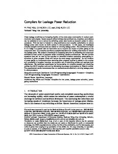
2.2 Controllability Lists Controllability lists give the information about the constraints on the input vector that are needed to make the node to reach a specific required state. Controllability lists can be calculated for each node in a large circuit and they can be tabulated as shown in Table 1. A simple benchmark ISCAS circuit C17 is taken as shown in Fig. 1 for testing the algorithm. The above Table 1 shows the controllability and the controllability lists for each node in the circuit. For example, take the node N6. The inputs to gate C1 are primary inputs. So, they have the controllability of 1. Now for the node N6 to gain logic 0 state, it is needed that both the inputs of the gate C1should be at logic 1 state. Hence, CC0 (N6) = 2 and CC0_list (N6) is (P0P1P2P3P4) = (xx11x), where x denotes a do not care condition. Similarly, for the node N6 to gain logic 1 state, one of the inputs to the gate C1 should be at logic 0 and thus CC1 (N6) = 1. In order to get the controllability list, the fan-out of each of the input nodes will be calculated and the node with a lower fan-out will be selected, which in the case of N6 is the primary input P3. Thus, the controllability at 1 list for node N6 will be CC1_list (N6) = (xxx0x). Similarly the controllability and the controllability lists for all the nodes can be calculated. Table 1: Controllability Lists for all nodes in C17 Net
CC0
CC1
N5
2: (1x1xx)
1: (0xxxx)
N6
2: (xx11x)
1: (xxx0x)
N7
2: (x1x0x)
1: (x0xxx)
N8
2: (xxx01)
1: (xxxx0)
Z0
2: (00xxx)
2: (1x1xx)
Z1
2: (x0xx0)
2: (xxx01)
Table 2 shows the leakage currents for a NAND gate in 180nm technology. It is observed that L00 and L10 are smaller compared to L01 and L11, where Lij denotes the total leakage (i.e. gate and sub-threshold leakage) in the P0 = i and P2 = j state. Hence, if x0 pattern is applied at the input of a NAND gate, the total leakage current will be less. In the similar manner the constraints for any type of the gate can be determined. Using the controllability lists these constraints can be mapped onto the primary inputs. Thus, Good Input Condition (GIC) for each gate gives the information about the input pattern that is to be applied that gets the gate to its low leakage state. For example, the constraint for gate C4 can be taken as (N5N7) = x0. Hence, its Good input condition (GIC) can be calculated as: GIC (C4) = Constraint (N5 = x) & CC0_list (N7) GIC (C4) = (xxxxx) & (x1x0x) GIC (C4) = (x1x0x)
2.4 Bad Input Condition (BIC) Similarly, Bad input condition list for each gate can be calculated. From Table 2, highest leakage state for a NAND gate is the 11 state. Thus, Bad Input Condition (BIC) for gate C4 can be taken as (N5N7) = (00xxx). The Good and the Bad input condition for each of the gates in C17 are given in Table 3.
2.5 Gate Leakage Penalty (GLP) If a gate input is not the GIC, then the gate may be in the high leakage condition. Then the gate leakage penalty will be calculated. Gate leakage penalty is the measurement of the increase in the leakage of the gate from the GIC. Gate leakage penalty (GLP) can be calculated by the difference in the mean leakage of the undesired high leakage states and the mean leakage of the low leakage states. Thus, GLP for a NAND Gate can be written as, GLP (NAND2) = 0.5*(L01 + L11) – 0.5*(L00 + L10)
2.3 Good Input Condition (GIC) For every gate in the circuit, the leakage depends on the input pattern given to that gate. Table 2 shows the total leakage for all possible input combinations for a NAND gate. Simulation is performed in CADENCE SPECTRE simulator for calculating the leakage current for all the input combinations of a NAND gate.
Table 2: Total leakage current for all possible input patterns for a NAND gate. P0
P2
L i j (pA)
0 0
0 1
2.69 9.19
1 1
0 1
8.75 14.92
Fig. 1: ISCAS benchmark circuit C17.
2.6 Bad Leakage Penalty (BLP) If a gate input is the bad input condition (BIC) then the gate may be in the worst leakage state and this increase can be measured by using Bad leakage penalty.
25
International Journal of Computer Applications (0975 – 8887) Volume 94 – No.7, May 2014 The difference between the highest leakage of the gate and the mean leakage of the low leakage states is called the Bad Leakage Penalty (BLP). BLP (NAND2) = L11 – 0.5*(L00 - L10)
Table 3: Constraint list for all gates in circuit C17 Gate
Good Input Condition
C0
(P2= 0) => xx0xx
C1
(P3=0) => xxx0x
C2
(N6=0) => xx11x
C3
(P4=0) => xxxx0
C4
(N7=0) => x1x0x
C5
(N8=0) => xxx01
Bad Input Condition (P0 = 1) & (P2 = 1) 1x1x x (P2= 1) & (P3= 1) xx11 x (P1= 1) & (N6= 1) x1x0 x (N6= 1) & (P4= 1) xxx0 1 (N5= 1) & (N7= 1) 00xx x (N7= 1) & (N8= 1) x0xx 0
2.7 Dominating Gates The states of the internal nodes can be known by the functionality of the gates in the given circuit for any input vector. For example, if necessary changes are made to satisfy the good input condition for any gate Cx, it may be possible that the good input condition (i.e. lowest leakage state) of another gate Cy is also satisfied with the changes that are made for the gate Cx. In this case, gate Cy is said to be dominated by the gate Cx. It is similar to the dominant faults used in the testing mechanisms [11].
2.8 Conflicting Gates Similar to the dominating gates, if the gate Ca is made to enter into its lowest leakage state then it may be possible that the particular input vector which made the gate Ca to enter into its lowest leakage state may force the gate Cb to its high leakage state. In this case, the gate Cb is said to be conflicting gate for gate Ca. For example, for the circuit C17, gates C1 and C2 are conflicting gates (since they have opposing necessities for the primary input P3). And gate C1 dominated by the gate C5 (since input pattern for gate C1 is a subset of the input pattern for gate C5). Like this, the conflicting and dominating gates for each gate can be tabulated as shown in Table 4.
Table 4: Dominating and Conflicting Gate List for all gates in the benchmark circuit C17 Gate
Dominated Gates
Conflicting Gates
C0
---
C2
C1 C2 C3 C4
------C1
C2 C0 , C2 , C4 , C5 C1 C2
C5
C1
C2 , C3
2.9 Work Function If the Good input condition (GIC) of a gate is satisfied, the GIC of its conflicting gates are unsatisfied and the GIC of its dominated gates are satisfied. Hence the work needed to be done for satisfying the good input condition of a gate(i) can be measured using its list of dominating gates and conflicting gates and their gate leakage penalties as follows: Work function (Ci) = ∑ (GLP (conflicting gates(C i))) - ∑ (GLP (dominating gates(Ci))) – GLP (Ci).
3. PROPOSED ALGORITHM FOR DETERMINING LOW LEAKAGE INPUT VECTOR It is observed that the sum of the leakage of the individual gates gives the total leakage of the circuit. So, if the leakage of the individual gates is reduced i.e. making them to enter into their lowest leakage states, the leakage of the whole circuit can be reduced. So, if all the gates are in their lowest leakage states then the total leakage of the whole circuit will be least. But forcing all the gates into the lowest leakage states may not be possible because of the inter dependencies of the gates. In this algorithm, it is tried to satisfy the good input condition for gates in the circuit while reducing the gate leakage penalty that comes due to the other gates whose good input condition is not satisfied. The algorithm to determine the lowest leakage input vector is given below: 1.
For each node in the given circuit, we will calculate the controllability and the controllability lists. 2. For each gate in the circuit, tabulate the input constraint lists and determine the list of dominating and conflicting gates. 3. Take all the gates into a required list 4. Until the required list has no gates in it, Calculate work function for each gate in the required list Take an input vector with all do not care conditions in it. 5. If the work functions are not zero and if more than one gate has the same least work function then update the input vector by doing AND operation with the input vector of the least indexed gate before removing it from the required list. Update the chosen gate with the next higher indexed gate and continue this step until only one gate has the least work function so that it will be taken as the chosen gate before continuing from step 7. 6. Else, take the gate with least work function and update the input vector by doing AND operation with the input vector of the chosen gate. Then continue from step 7. 7. Remove the chosen gate and its list of dominating gates from the required list. 8. Remove the list of its conflicting gates from the required list and place them in the violated list. 9. Update the dominating and conflicting gate list for each gate. 10. If any input is not defined Set undefined input to 1 and calculate Work-Input(1) = ∑ (BLP (Violated gates that get their BIC satisfied)
26
International Journal of Computer Applications (0975 – 8887) Volume 94 – No.7, May 2014
Fig. 2: ISCAS C17 Circuit in CADENCE VIRTUOSO
Set undefined input to 0 and calculate Work-Input(0) = ∑ (BLP (Violated gates that get their BIC satisfied) Assign input to suitable value based on Work-Input(0) and Work-Input (1)
11. End. The procedure of choosing the gate with the least work function guarantees that in each looping step the most useful input pattern (least leakage penalty) is satisfied first. In order to reduce the number of violated gates that have their BIC satisfied, the undefined inputs can be given a suitable state. The number of iterations is reduced by one in the proposed algorithm when compared to the one given in [10]. So, it takes less time to execute than in [10]. The final input pattern is a least leakage input vector that can be applied to the circuit in the sleep state. For example, to determine the least leakage vector for the circuit C17, the input constraint lists, controllability lists and the list of dominating and conflicting Gates can be tabulated (as shown in Tables 3,1 and 4). The initial required list contains all the gates in the circuit and the initial vector is completely not specified. In the first iteration of the choosing loop, gate C 4 is chosen as the best gate since it has least work function as it has one conflicting gate (C2) and one dominating gate (C1) (and all other Gates are identical and hence have the same GLP). So, input vector is updated with the input pattern of the gate C 4 and the required list is reduced by deleting the gates C4, C1 and C2. Then in the next iteration, gates C0 will have the least work function but the next gate C3 will also have the same work function as C0. So, the gate C0 will be removed from the list and the gate C3 will be the chosen gate. So the input vector is updated with the input pattern of the gate C3. Steps 4 to 9 are then repeated until the required list contains no gates as shown in Table 5. The output waveform of the C17 circuit for different combinations of the input patterns is shown in Fig. 3.
The C17 circuit is designed with proper adjustments of w/l ratios in CADENCE and the output has been taken. The circuit in CADENCE is shown in Fig. 2.
4. RESULTS Table 5 gives the information about the chosen gate and the input vector after each iteration in the proposed algorithm.
Table 5: Chosen Gate and input vector after each iteration for the circuit C17
Iteration
Input Vector
0
Chosen Gate ------
1
C4
x1x0x
2
C3
x1000
xxxxx
Required List C0, C1, C2, C3, C4, C5, C0, C3, C5 ------
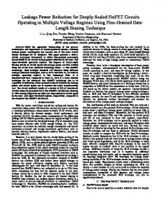
The algorithm has been implemented in C and it was checked with an ISCAS benchmark circuit C17. The results are compared against the best vector (which has least leakage current value) after checked with all the possible input combinations in CADENCE SPECTRE. A graph of the leakage current values for all the combinations of inputs is shown in Fig. 3 for the circuit C17 designed in 180nm technology. It is observed from the Fig. 3 that the input vector 8 i.e. 01000 has the minimum leakage value among all the 32 combinations of the input patterns. That means the vectors obtained from the last iteration of the proposed algorithm i.e. x1000 and from the CADENCE simulations are same. Leakage current values obtained here are in femto amperes. The number of iterations of the algorithm given in this paper will be less compared to the one given in [10].
27
International Journal of Computer Applications (0975 – 8887) Volume 94 – No.7, May 2014
Fig. 3: Leakage Current Values for all the input combinations for the circuit C17
In particular, for the circuit taken in this paper i.e. C17; the complexity has been decreased by one iteration. This algorithm can be modified to determine the higher leakage input vector by changing the input constraint values. Thus, the proposed algorithm can be used to calculate the range or boundaries of leakage current in any given circuit.
[2] L. Wei, et.al, “Design and optimization of low voltage high performance dual threshold CMOS circuits,” Proc. Of DAC, pp. 489-494, Jun. 1998.
5. CONCLUSIONS
[4] T. Kurado, et.al, “A 0.9V, 150 MHz, 10-mW, 4mm2, 2-D Discrete Cosine Transform Core Processor with Variable Threshold (Vt) Scheme,” IEEE Journal of Solid Stare Circuits, vol. 3 1, no. 11, pp. 1770 - 1779, Nov. 1996.
If a low leakage input vector is applied then the total leakage of the circuit can be minimized in the sleep state. In this paper, an algorithm which determines the least leakage input vector was given. It uses the concept of controllability of the nodes and also uses the functional dependencies among the gates in the circuit to search the required input vector. The results shows that the algorithm can determine the vector that gives a low leakage value which is nearer to the value (almost same) obtained using the exhaustive searching of low leakage value for all possible input combinations for the circuit designed in CADENCE SPECTRE, the execution time of the proposed algorithm is less as one iteration is reduced when compared to the algorithm given in [10]. This algorithm can be applied to any combinational circuit to evaluate the boundaries of the leakage current with some modifications while calculating the highest leakage vector.
6. ACKNOWLEDGEMENT The authors would like to thank the authorities of MANIT Bhopal for providing the CADENCE tool without which the completion of this project would not be possible. Authors would also like to thank the members of department of ECE in MANIT Bhopal for their valuable discussions and suggestions.
7. REFERENCES [1] Behnaz Mortazavi, “Modeling leakage in sub-micron CMOS technologies” Azad University of Tehran-Iran, Jun. 1995.
IJCATM : www.ijcaonline.org
[3] S. Mutoh, et.al, “I-V Power Supply High-speed Digital Circuit Technology with Multi-Threshold Voltage CMOS”, IJSSC, vol. 30, no. 8, pp. 847-854, Aug. 1995.
[5] F. Assaderaghi,“DTMOS: Its Derivatives and variations, and their Potential Applications,” Proc. of 12th Intnl. Conference on Microelectronics, pp. 9-19, 2000. [6] D. Duarte, Y. Tsai, N. Vijaykrishnan and M. Irwin, “Evaluating Run-Time Techniques for Leakage Power Reduction,” Proc. Of 15th Intnl. Conjerence on VLSI Design, pp. 31-38,2002 [7] J. Halter and F. Najm, “A Gate-Level Leakage Power Reduction Method for Ultra Low Power CMOS Circuits,” Proc. Of ClCC, pp.475-478, 1997. [8] Abdoul Rjoub , “ A fast input vector control approach for sub-threshold leakage power reduction”, Almotasem Bellah Alajlouni, Hassan Almanasrah, 2012. [9] Nikhil Jayakumar, “ An algorithm to minimize leakage through simultaneous input vector control and circuit modification”, Sunil P Khatri, Texas, 2007. [10] A heuristic to search a low leakage vector for CMOS circuits”, Rahul M.Rao, Frank Liu, Jeffrey L.Burns, Richard Brown, Austin research labs, 2006. [11] M. Abramovici, M.Breuer, A.Friedman, “Digital Systems Testing and Testable Design”, IEEE Press, 1995.
28