AN ASIC PERSPECTIVE ON FPGA OPTIMIZATIONS Andreas Ehliar, Dake Liu Department of Electrical Engineering Link¨oping University Sweden email:
[email protected],
[email protected] ABSTRACT In this paper we discuss how various design components perform in both FPGAs and standard cell based ASICs. We also investigate how various common FPGA optimizations will effect the performance and area of an ASIC port. We find that most techniques that are used to optimize a design for an FPGA will not have a negative impact on the area in an ASIC. The intended audience for this paper are engineers charged with creating designs or IP cores that are optimized for both FPGAs and ASICs. 1. INTRODUCTION FPGAs are becoming more and more common and are used in both high and low-end systems. In some cases it is easy to meet the performance and area goals using non-optimized generic HDL code. This is not true as often as designers would like and various FPGA specific tricks are often required to either meet timing or fit the design into the selected FPGA. If the design is intended for a high volume ASIC product where the FPGA version is only used for prototyping it is probably not a big problem since such a design does not usually have to be optimized for the FPGA. However, when the design is intended for high volume production using FPGAs and a future ASIC port if the FPGA based product is successful, the ease of ASIC portability is very important indeed. This is the scenario which the rest of this paper will investigate. 2. RELATED WORK It is surprisingly difficult to find information about porting FPGA designs to ASICs, especially with regards to various FPGA optimization. While it is likely that various consulting firms specializing in FPGA to ASIC migrations have internal documents on this subject, very few publications are available that discusses this. A brief overview of how to port an FPGA design to an ASIC is given in [1]. The opposite problem, migrating an ASIC design to an FPGA is better documented and guidelines about this can be found
from the FPGA vendors [2]. Many of these guidelines are also applicable when creating an FPGA design which will be migrated to an ASIC. Finally, FPGA versus ASIC design trade-offs have also been discussed by us previously in [3]. An interesting comparison of the performance difference between ASIC and FPGAs is given in [4] where the performance, area and power consumption of a 90 nm ASIC and a 90 nm FPGA is measured. The benchmarks selected by the authors in this paper do not seem to include designs that are specifically targeted and optimized for FPGAs though. There are also a few publications with information about structured ASICs and how to port an FPGA design to such products such as [5] and [6]. The relatively fixed structure of these solutions means that not all of the information is applicable to a true standard cell based ASIC port though. 3. METHODS It is not our intention to crown the fastest or most area efficient FPGA. Therefore we have decided to use relative performance and area cost numbers in this paper. All numbers are therefore relative to the performance and area of a 32-bit adder in the selected technology. Another reason to use relative numbers is to protect proprietary information like the exact size and performance of ASIC memory blocks. One problem with any comparison of this kind is that it is not really clear what area means in the context of an FPGA design since it can contain components like block rams and DSP blocks in addition to LUTs and flip-flops. One possible metric is simply to measure the silicon area of the various components in the FPGA, which is basically what was done in [4]. While this comparison is very interesting from an academic point of view, it is not very useful to a VLSI designer (unless employed by an FPGA manufacturer). 3.1. FPGA Area Cost We propose another metric for the area cost which we will use in this paper. First of all, we assume that flip-flops and LUTs will be packed as tightly as possible into slices. Sec-
ondly, we set the slice cost for a block RAM as the total number of slices in the device divided by the total number of block RAMs in the device. If a device have block RAMs of several sizes (like in Stratix III), the large block RAM is measured as if it was several small block RAMs. The slice cost for a DSP block is derived similarly except that we also have to take into account whether only part of the block is used. For example, a DSP block in the Stratix III can be divided into independent 9, 12, 18, and 36-bit multiplier blocks where the smaller multipliers are used to create larger multipliers. The advantage is that this metric is easily calculated for all FPGAs and it is easily understandable for a VLSI designer. In addition, assuming that the designer values all features of a certain FPGA equally (or at least roughly equally) this area cost metric will be a good indication of the monetary value of a certain kind of design element. However, as we realize that this metric may be controversial to some readers we will also note whenever an area cost figure is based upon this kind of conversion. 3.2. Design Flow and Tools The tools used to synthesize the FPGA designs in this paper were ISE 10.1 and Quartus II 8.1 for Xilinx and Altera respectively. To find the maximum frequency (Fmax ) we followed the advice given in [7] which recommends that the timing constraints were increased until timing could no longer for Xilinx designs and that the timing constraints are over-constrained to 1 GHz for Altera designs. Synopsys Design Compiler (A-2007.12-SP5) was used for ASIC synthesis and Cadence SoC Encounter (v5.20) was used for ASIC place and route. The selected ASIC technology is a standard cell based 130 nm technology based on the comparably low NRE costs and the fact that this is still a very popular technology node for new design starts [8]. The static timing analysis for the ASIC is based upon worst case parameters. Due to the many possibilities to trade area for frequency in ASICs we have also included numbers based on both speed and area optimized designs. 4. PERFORMANCE AND AREA COST OF IMPORTANT COMPONENTS This section contains a comparison of the relative cost of various common constructs in an FPGA and in a 130nm ASIC process. Table 1 shows an overview of the relative costs of selected components. The Spartan 3A (xc3s700a), Virtex 5 (xc5vlx85), Cyclone 3 (EP3C40), and Stratix 3 (EP3SL150), was used in this comparison. In all comparisons, the fastest speedgrade was used. (As a side note, this table alone should show how futile it is to try to estimate the gate count in an ASIC by counting LUTs in an FPGA design.)
4.1. Adders and Subtracters Adders are one of the most common components in any digital design. It is also a component which the architecture of most FPGAs are optimized for by the use of dedicated carrychains. For this reason an adder in an FPGA tends to be a pretty simple component which is usually using one LUT per bit and there is little reason to deviate from this template (except pipelining of very large adders and using bit-serial adders for non-performance critical tasks). However, when using ASICs, the area of an adder can vary widely depending on the timing constraints as seen in Table 1. It can also be seen that an ASIC enjoys an advantage for situations which the FPGA is not optimized for, such as multi-operand adders. (Although it is interesting that the architecture of the Stratix III allows a 3-operand adder to be created without any area penalty.) 4.2. Multiplexers Multiplexers and similar structures is a very common design component. The performance of multiplexers in an FPGA is usually high due to the use of specialized logic in the FPGAs such as the MUXF5-8 components in most Xilinx FPGAs. On the other hand, the area cost for multiplexers is very high when compared to the cost of the adders as shown in Table 1. This means that trade-offs that are valid in an FPGA such as avoiding the use of crossbar based SoC interconnects may no longer be valid in an ASIC. If a SoC system is well designed, replacing a SoC bus, such as Wishbone or AMBA, with a crossbar may be a fast way to raise the performance of an ASIC port without a costly redesign/reverification. FPGA and ASIC optimization hint Multiplexers are expensive in FPGAs and cheap in ASICs. The performance of an ASIC can sometimes be enhanced at little area cost by strategically placed multiplexers, such as using crossbars instead of buses. 4.3. Multipliers and DSP blocks If an FPGA is used which does not have any built-in multipliers, the ASIC is clearly going to be much more resource efficient. When built-in multipliers are added to the equation, it is possible that the performance of an ASIC port will actually be slower than the FPGA, since the multipliers in the FPGA are well optimized and in many cases also enjoy a technology node advantage over the ASIC based multiplier. On the other hand, the ASIC process enjoys a huge advantage as soon as a nonstandard multiplication size is used. Going from 17×17 to 19×19 is very costly in the FPGA, whereas the area cost difference in ASICs are low and the performance difference is negligible. Similarly, architectures that do not map efficiently to DSP blocks will also gain performance when ported to an
Table 1. Relative area and performance of common components Design Relative area cost (lower is better) Relative Fmax (higher is better) (Note that all designs FPGAs ASIC4 FPGAs ASIC4 have registered outputs) xc3s700a xc5vlx85 ep3c40 ep3sl150 (130 nm) xc3s700a xc5vlx85 ep3c40 ep3sl150 (130 nm) 32-bit adder 1.0 1.0 1.0 1.0 1.0 ( 0.21) 1.0 1.0 1.0 1.0 1.0 ( 0.11) 32-bit adder/subtracter 1.0 1.0 2.0 1.0 1.9 ( 0.25) 0.97 0.90 0.82 0.81 0.89 ( 0.13) 32-bit 3 operand adder 1.9 1.9 2.0 1.0 1.3 ( 0.40) 0.86 0.82 0.77 0.89 0.74 ( 0.12) 32-bit 4 operand adder 2.9 2.9 3.0 2.0 1.7 ( 0.55) 0.62 0.58 0.77 0.82 0.69 ( 0.10) 32-bit 16-to-1 mux 8.0 5.0 10 5.0 0.57 ( 0.48) 1.5 0.92 1.3 1.7† 0.90 ( 0.31) ∗ ∗ ∗ ∗ 17x17 unsigned multiplier 18 34 10 19 3.7 ( 1.3) 1.3 0.64 0.81 0.61 0.44 ( 0.11) 19x19 unsigned multiplier 75∗ 35∗ 36∗ 37∗ 4.1 ( 1.6) 0.46 0.40 0.59 0.49 0.43 ( 0.10) 18x18 MAC unit (Fig. 1a) 25∗ 35∗ 19∗ 26∗ 5.3 ( 2.4) 0.55 0.41 0.51 0.53 0.42 ( 0.08) ∗ ∗ 18x18 MAC unit (Fig. 1b) 29 35 21∗ 42∗ 5.4 ( 2.7) 0.79 0.82 0.77 0.62 0.49 ( 0.11) 18x18 MAC unit (Fig. 1c) 25∗ 36∗ 24∗ 29∗ 4.9 ( 2.7) 0.75 0.72 0.63 0.62 0.49 ( 0.09) 2048x32 bit memory 74∗ 34∗ 79∗ 57∗ - ( 33‡ ) 1.5 0.72 0.75 0.92 - ( 0.53‡ ) ∗ † † RF (16x32 bit register file) 1.0 1.0 10 2.1 2.7 ( 2.5) 2.1 1.2 0.74 1.0 0.93 ( 0.31) RF (Ports: 1 read, 1 write) 2.0 1.0 10∗ 2.1 2.6 ( 2.5) 1.9† 1.1 0.73 1.2 0.93 ( 0.23) RF (Ports: 2 read, 1 write) 4.0 2.0 20∗ 4.3 3.2 ( 3.0) 1.9† 1.0 0.74 1.0 0.89 ( 0.22) RF (Ports: 4 read, 2 write) 50 40 59 21 5.8 ( 4.6) 0.97 0.66 0.90 1.1 0.91 ( 0.13) 4 Values in parentheses are from designs optimized for area ∗ Relative area cost includes DSP or RAM blocks (See Section 3.1) † Exceeds maximum frequency of clock net as reported in the datasheet. ‡ The ASIC memory block was only optimized for area.
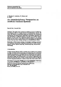
a
x
Mem 4 x 48
Mem 4 x 48
x Mem 4 x 48
b
x
c
a) Plain MAC b) MAC with a pipelined adder c) MAC with a pipelined adder and forwarding Parts marked in grey are mapped to the DSP48E block.
Fig. 1. MAC units mapped to DSP48E blocks ASIC. Take for example the Multiply-accumulate unit in Table 1 (also shown in Fig. 1a. The multiplier in this example is 16×16 bits and the 4 accumulator registers contain 48 bits each. While the multiplier fits the DSP48E of the Virtex-5 very well, the design will have suboptimal performance as the accumulation register in the DSP48E cannot be used. An alternative is shown in Fig. 1b where the adder of the MAC unit has been pipelined. This architecture is only limited by the performance of the DSP48E block. The drawback of this architecture is that the pipelining means that it is no longer possible to accumulate to the same register at all times as is possible in Fig. 1a. A compromise is the solution shown in Fig. 1c where result forwarding is used to achieve the same functionality as in Fig. 1a. The performance of this architecture is not as high as in Fig. 1b, but it is substantially higher
than the performance of the plain MAC. On the other hand, in the ASIC, the performance of all three options are similar. (See also the discussion in Section 5.3.) FPGA and ASIC optimization hint If the design has been specifically optimized for the DSP blocks in the FPGA, it is likely that there will be performance problems when porting the design to an ASIC. 4.4. Large Memories When synthesizing a design with large memory blocks for an ASIC it is necessary to use memories that are optimized for that particular ASIC process. If this is not done the area and performance of the design will be abysmal (in a simple experiment we performed, a standard cell based 8 KiB memory was 10 times larger than a custom memory block). While it is critical to use specialized memories for anything but the smallest memory, there is surprisingly little publicly available information about ASIC memory blocks. One datasheet which does contain area and frequency information is available from Atmel for a 0.35 µm process [9]. According to this datasheet, a dual port memory is roughly 60% larger than a single port memory. While we would prefer to refer to publicly available information for newer technologies, it is nevertheless clear that it is significantly more area expensive to use a dual port memory than a single port memory. Therefore it makes sense to avoid dual port memories in ASICs if the same performance can be reached using single port memories. As an example of this, FIFOs are usually implemented using dual port memories in an FPGA even though a synchronous FIFO can be implemented using
only single port memories as described in for example [10]. If it is not easy to avoid a dual port memory it is necessary to consider the cost and time required to redesign the system (if possible) and compare that against the cost of the increased ASIC area that dual port memory usage will lead to. For memories which contain read-only information it can also be a very good idea to use a ROM compiler instead of an SRAM. Not only does this avoid the problem of initialization, a ROM is also much smaller than an SRAM. In [9] for example, a 1 kilobyte 8-bit wide ROM is about 1/7 the size of a (single port) RAM with similar size. FPGA and ASIC optimization hint It is extremely important that memory generators are used for large memories in an ASIC. Significant area savings are also possible if some of the memories can be created using ROM-compilers. Finally, dual port memories should not be used if it can be avoided. 4.5. Small Memories When using small memories in an ASIC it is still possible to use specialized memory modules (commonly referred to as register file memories) although this is not as critical as when using a large memory. Unless a large amount of register files are used in the design, the increased implementation and verification cost of using specialized ASIC memories might not be worth it. As can be seen in Table 1, FPGA based designs are usually fairly efficient when using small single and dual-port memories. A configuration of two read ports and one write port is also fairly efficient. As soon as more than one writeport is used, the synthesis tool for the FPGAs are no longer able to utilize distributed memory and has to resort to using flip-flops with a significant area increase. FPGA and ASIC optimization hint Small register files with one write port and few read ports are typically more area efficient in most FPGAs. If register files with more than one write port is used, they are likely to be much more area efficient in an ASIC. 5. FPGA OPTIMIZATIONS AND THEIR IMPACT ON AN ASIC There are many optimizations that can be done on a design to improve the performance in an FPGA. In the end they can all be summarized as modifying the architecture of the design to better fit a given FPGA. This section will classify these optimizations and discuss their impact on an ASIC. 5.1. Deep Pipelining Perhaps the most important tool in an FPGA designer’s toolbox is pipelining. While pipelining is also beneficial for the
Table 2. Relative area/frequency of an eight point 1D DCT pipeline for various pipeline depths. Pipeline Relative area Relative Fmax stages xc3s700a ASIC4 xc3s700a ASIC4 ∗ 1 260 20 (5.5) 0.25 0.30 (0.073) 2 260∗ 13 (6.1) 0.33 0.35 (0.079) 3 260∗ 14 (6.8) 0.38 0.41 (0.10) 4 260∗ 13 (7.0) 0.37 0.40 (0.10) 4 Values in parentheses are from designs optimized for area ∗ Relative area cost includes DSP blocks (See Section 3.1)
performance of ASICs in all but the most pathological cases, it is not always a good idea in terms of area. As an example of how pipelining effects the area and performance, an ASIC based 16×16 speed optimized multiplier with 4 register stages was 12.6% percent larger and 37.9% faster than the same multiplier with only 1 register stage. Adding a pipeline stage is not guaranteed to increase the area though. This is seen in Table 2 where an eight point 1D DCT pipeline (without FPGA optimizations) has been synthesized using different number of registers. In this example, the synthesis tool is clearly struggling to meet timing when only one pipeline register is available. FPGA and ASIC optimization hint While pipelining an FPGA design will certainly not hurt the maximum frequency of an ASIC, the area of the ASIC will often be slightly larger than necessary, especially if the pipeline is not a part of the critical path in the ASIC. 5.2. Utilizing Slices Efficiently Another important task when optimizing a design for an FPGA is to select the architecture so that it is possible to utilize the slices efficiently. For example, in a Spartan-3, a 32-bit adder will use 32 LUTs. At the same time it is also possible to fit a combined 32-bit adder/subtracter or a 32-bit adder with a 2-to-1 mux in front of one of the operands using only 32 LUTs. This is exemplified in Table 3 where a 32bit adder in a Spartan-3 is compared with adders with extra functionality. If the relative area of a certain Spartan-3 based design is 1.00, this means that it is possible to combine all functionality into only one LUT / bit. The maximum frequency is more or less the same as that of a plain adder. For the ASIC based designs, the maximum frequency is lowered in all cases when compared to the plain adder and the area is almost always increased. This means that if even a single adder in the design is combined with extra functionality it is very unlikely that the performance of the design will equal that of a plain adder. On the other hand, the ASIC port will have an area advantage as soon as functionality that cannot fit into a single LUT / bit is used. On the Spartan-3 this happens when for example a 2-input bitwise or function for both operands of an adder are used or when combining a 2-to-1
Table 3. Combining an adder with other functionality Relative area Relative Fmax xc3s700a ASIC4 xc3s700a ASIC4 Plain add 1.00 1.00 (0.21) 1.00 1.00 (0.11) One 2-to-1 mux 1.00 1.15 (0.25) 0.99 0.69 (0.14) Two 2-to-1 mux 2.03 1.20 (0.30) 0.85 0.67 (0.14) Two 2-input 1.97 0.82 (0.27) 0.84 0.85 (0.11) bitwise or Two 2-input 1.00 0.89 (0.27) 0.99 0.89 (0.11) bitwise and 32-bit adder Relative area Relative Fmax and subtracter xc3s700a ASIC xc3s700a ASIC Plain add/sub 1.00 1.66 (0.25) 1.00 0.86 (0.14) One 2-to-1 mux 2.03 1.37 (0.31) 0.82 0.69 (0.14) Two 2-to-1 mux 2.97 1.39 (0.36) 0.85 0.64 (0.12) 4 Values in parentheses are from designs optimized for area 32-bit adder
Table 4. Inferring and instantiating components Design Relative area Relative Fmax Virtex4 ASIC Virtex4 ASIC Mux (Inferred) 4.38 0.57 1.3 0.95 (Instantiated) 4.50 0.64 1.3 1.07 Add/sub (Inferred) 1.00 1.86 0.98 0.89 (Instantiated) 1.00 1.42 0.98 0.76 MAC(Instantiated) 118∗ 16.2 1.19 0.40 (Rewritten) 10.7 0.70 ∗ Relative area cost includes DSP blocks (See Section 3.1)
mux with an adder/subtracter. FPGA and ASIC optimization hint Careful design can allow an FPGA design to combine adders with extra functionality without any performance or area impact. The timing budget of an FPGA design where all adders are optimized like this can be derived from the maximum frequency of an adder. For the ASIC port this is not possible and the extra functionality has to be taken into account. 5.3. Manual Instantiation of FPGA primitives Synthesis tools are getting better with each version, but there are still some cases where it may be necessary to instantiate slice primitives like LUTs and flip-flops manually. One reason to do this is when the synthesis tool creates suboptimal logic for a critical path, another reason is that the designer needs to ensure a consistent naming scheme for floorplanning reasons. Once FPGA primitives are manually instantiated the design is no longer directly portable to an ASIC. It is on the other hand fairly easy to write a portability library with synthesizable code for FPGA primitives like lookuptables, flip-flops, carry chain primitives, etc. This allows such a design to be synthesized to an ASIC with surprisingly good results as long as the designs are flattened during the
optimization phase of the synthesis flow. Table 4 shows the performance of a few typical types of circuits when inferred and instantiated. It is expected that the mux based on LUTs and MUXFx components would have roughly the same performance as an inferred mux but it is quite surprising that the performance of the adder/subtracter based on LUTs, MUXCy, and XORCy components is only around 15% worse than an inferred adder. Intuitively, the instantiated adder should have a fairly low performance in an ASIC since it is basically a ripple-carry adder, but the synthesis tool is obviously able to optimize the combinational paths of the ripple-carry adder so that the final end result is an optimized adder instead of a plain ripple-carry adder. Finally, the MAC component is a 32×32 bit MAC unit based on four DSP48 blocks. (Because of the exact semantics of such a MAC unit where the P registers hold partial results,it is not easy to infer such a component without essentially duplicating parts of the DSP48 blocks, therefore no inferred value is reported.) As we can see, the performance is on par with the plain 17×17 multiplier from Table 1. However, by rewriting the MAC unit to use a pipelined DesignWare multiplier and changing the semantics to avoid the use of partial results in the accumulator, the ASIC performance can be increased by almost 75% while decreasing the area. FPGA and ASIC optimization hint If FPGA primitives are instantiated manually in the HDL source code it is still possible to create an ASIC port by using a small compatibility library with synthesizable versions of these primitives. There may be a loss of performance when using this method, especially when instantiating larger components like DSP blocks and our recommendation is therefore to avoid primitive instantiation unless the gains are huge. Nevertheless, if this approach is used, it is imperative that the design is flattened during synthesis before the optimization phase! 5.4. Manual Floorplanning and Routing Although floorplanning is not commonly used in FPGA design it can be a powerful tool. In theory this should have no impact on an ASIC port. In practice it may be necessary to modify the HDL source code to manually instantiate LUTs and other primitives to ensure that the floorplanning will be valid even if synthesis options or synthesis tools are changed. Although manual routing is rarely done in practice, the same reasoning is true here as well. FPGA and ASIC optimization hint Manual floorplanning will itself have no impact on an ASIC port. However, it is likely that a design has to be modified to simplify floorplanning. In that case these modifications have to be assessed for ASIC portability.
6. MICROPROCESSOR CASE STUDY As a case study, we ported our xi2 soft-core processor optimized for the Virtex-4 [11] to an ASIC process. Around 11% of the flip-flops and 18% of the LUTs in the processor are manually instantiated, either to simplify floorplanning or because the synthesis tool did not infer the desired logic. The block RAMs and DSP blocks are also manually instantiated to ensure a consistent naming scheme for floorplanning. The processor pipeline is well balanced in the FPGA and there is very little slack available in any pipeline stage. A first attempt to port the design using a compatibility library resulted in a design which was actually slower in the ASIC than in the Virtex-4. Contrary to our first expectations, we never had any timing problems with the manually instantiated slice components (including carry chains in the arithmetic unit). All critical paths in the first ASIC port was instead located in the DSP48 based MAC unit. (See also Section 5.3.) After this unit was totally rewritten using DesignWare components, the maximum frequency of the ASIC port increased by 54%. The new critical path is instead caused by the memory blocks and could not be corrected without using power hungry high speed memory blocks. This experience supports the conclusion that manual instantiation of slice primitives is not a major problem when porting an FPGA design to an ASIC. Instead, the major problems are caused by DSP blocks and memory blocks. Other experiments we have done on FPGA optimized NoCs and floating point units also supports this conclusion [3]. 7. OTHER PORTING ISSUES An important issue which has not been discussed yet is the ability to reconfigure the FPGA. This is a powerful ability which can be used to for example reduce the area of a design, correct bugs or handle diagnostic testing (through specially created bitstreams). It is obvious that an ASIC port will be complicated if a design relies on the ability to reconfigure the FPGA. If nothing else, the difficulty of fixing bugs in the ASIC may force the designer to add functionality to the ASIC to make it possible to work around at least some bugs. There are also many other issues that have to be considered when porting an FPGA design to an ASIC that are not directly related to FPGA specific optimizations. This includes design for test, I/O, power dissipation and licensing terms for soft and hard IP blocks. A thorough treatment of these topics are out of the scope of this paper however. 8. CONCLUSIONS In this paper we have discussed how important design constructs perform in terms of area and maximum frequency in FPGAs and ASICs. We have also discussed how vari-
ous FPGA optimization techniques can be used. We conclude that most of these techniques are either beneficial or relatively non-harmful for the performance and area of an ASIC port. The most dangerous areas are memories and DSP blocks and extra care must be taken to make sure that an ASIC port is efficient, especially if a design has been specifically optimized for these FPGA components. 9. REFERENCES [1] C. Baldwin. Converting fpga designs. [Online]. Available: http://www.chipdesignmag.com/display. php?articleId=2545 [2] AN 311: Standard Cell ASIC to FPGA Design Methodology and Guidelines ver 3.0, Altera, 2008. [3] A. Ehliar, “Performance driven fpga design with an asic perspective,” Ph.D. dissertation, Link¨oping University, 2009. [4] I. Kuon and J. Rose, “Measuring the gap between fpgas and asics,” in Computer-Aided Design of Integrated Circuits and Systems, IEEE Transactions on, 2007. [5] M. Hutton et al., “A methodology for fpga to structured-asic synthesis and verification,” Design, Automation and Test in Europe, 2006. DATE ’06. Proceedings, vol. 2, pp. 1–6, March 2006. [6] J. Gallagher and D. Locke, “Build complex asics without asic design expertise, expensive tools,” 3 2004. [Online]. Available: http://electronicdesign. com/Articles/Print.cfm?AD=1&ArticleID=7382 [7] Altera, Guidance for Accurately Benchmarking FPGAs v1.2, 12 2007. [Online]. Available: http://www.altera.com/literature/wp/wp-01040.pdf [8] ——, “Wp-01089-1.0, power-optimized solutions for telecom applications,” 2009. [Online]. Available: http://www.altera.com/literature/wp/ wp-01089-power-optimized-telecom.pdf [9] Atmel, ATC35 Summary. [Online]. Available: http://www.atmel.com/dyn/resources/prod documents/1063s.pdf [10] D. Drako and H.-T. A. Yu, “Apparatus for alternatively accessing single port random access memories to implement dual port first-in first-out memory,” U.S. Patent 5 371 877, 12 6, 1994. [11] A. Ehliar, P. Karlstrom, and D. Liu, “A high performance microprocessor with dsp extensions optimized for the virtex-4 fpga,” Field Programmable Logic and Applications, 2008. FPL 2008. International Conference on, pp. 599–602, Sept. 2008.