of Magma Design Automation for valuable suggestions on. PTL synthesis and other useful interactions. References. [1] M. Alidina et al. Precomputation-Based ...
An Efficient Algorithm for Low Power Pass Transistor Logic Synthesis Rupesh S. Shelar, Sachin S. Sapatnekar Department of Electrical and Computer Engineering, University of �Minnesota, Minneapolis, MN 55455. Email: rupesh,sachin � @ece.umn.edu Abstract
tion [4, 5]. For power optimization of PTL circuits, Lindgren et al. propose the use of sifting [6] which reduces switching activity in BDD mapped PTL circuits [7]. Another approach by Tavares et al. proposes employing split cofactors based on the Shannon expansion at the root of BDD’s, with the variable corresponding to root node being used as a control input to disable the inverters [8]; the disabled inverters cannot make low-to-high transition, resulting in reduced switching activity. This approach differs from an approach of independent of cofactors by Alidina et al. in disabling inverters rather than disabling registers and also in algorithm as [1] uses area-efficient co-factors while [8] uses the power-efficient cofactors.
In this paper, we address the problem of power dissipation minimization in combinational circuits implemented using pass transistor logic (PTL). We transform the problem of power reduction in PTL circuits to that of BDD decomposition and solve the latter using the max-flow min-cut technique. We use transistor level power estimates to guide the BDD decomposition algorithm. We present the results obtained by running our algorithm on a set of MCNC benchmark circuits, and show on an average of 47% power reduction over these circuits; the comparison with the previously proposed low power pass transistor logic synthesis algorithms shows an average improvement of over 23% over the best previously published approach.
In this paper, we propose a BDD decomposition technique to minimize the power dissipation in combinational logic under the assumption that all primary inputs and primary outputs are registered. We use the switching probability estimation technique proposed in [7] to estimate the switching probabilities in PTL circuits and also take into account the capacitance driven by each node in the PTL circuit, unlike [7] which uses a linear fanout model. Unlike the previous approaches [1, 8], which use a single variable to disable the inputs of independent co-factors, we decompose the logic function using the max-flow min-cut technique to find the cut in the BDD that minimizes the power dissipation; the cut yields a subset of variables used as inputs to select logic that is used to disable the part of the circuit that does not perform useful computation in a given clock cycle. Our decomposition-based implementation model is more flexible than the bipartitioning codec architecture proposed in [3] and allows us to find optimum decomposition; optimality of decomposition is ensured due to the use of Ford-Fulkerson algorithm [9] to find the min-cut.
1 Introduction Power dissipation is becoming a critical problem in modern day deep sub-micron circuits, especially in case of circuits that are used in portable battery-operated devices. The problem of power optimization at various levels of abstraction has been addressed by numerous researchers. At the logic level, power optimizations include techniques such as gated clocks and precomputation; the latter include the use of the observability don’t cares to disable the clock signal at the input registers [1]. Using a similar approach, Ruan et al. propose bipartitioned codec architecture in which output values are encoded using the minimum number of bits, and then decoded using the decoder in the next clock cycle, or computed conditionally [2, 3]. A limitation of the precomputation scheme [1] is the addition of extra logic to the circuit, while the bipartitioning codec approach may not be always optimal. Among the recently popular logic families, pass transistor logic (PTL) is promising for low power applications as compared to conventional static CMOS because of its lower transistor count, lower capacitances due to the possible use of NMOS transistor as pass transistors and therefore, good performance and lower power dissipa�
The organization of the rest of the paper is as follows. In Section 2, we describe the power estimation technique used for PTL circuits. In Section 3, we illustrate the BDD decomposition and propose an algorithm for minimizing the power dissipation in Section 4. In Section 5, we discuss the experimental results obtained using the algorithm, followed by concluding remarks in Section 6.
This work was supported in part by SRC under award 99-TJ-692.
1
2 Power Model
(1/2,1/2,1/2)
f
(3/8,3/4,1/4)
a
b
a b
c
(a)
(3/8,3/4,1/4)
3Cs
3Cs
a’
b
b’
c
(1/2,1/2,1/2)
b
c’
(0,1,0)
4Cs
(0,0,1)
2Cs
2Cs
(a)
0
1
2Cs+C i
(b)
(b)
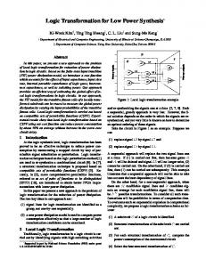
Figure 2. Power estimation in PTL circuits (a) Switching probability estimation, (b) Capacitance estimation.
Figure 1. Correspondence between a BDD node and its PTL implementation (a) BDD for f=ab+c(ab’+a’b), (b) Corresponding PTL Implementation.
clock frequency, ] LON and W LON are switching probabilities and capacitances, respectively. � 6ed"f�gih L ] LON W LON < Zlk � (4) ]_^B`ba�c [\j [\[
Figure 1(a) shows the BDD for the function f = ab+c(ab’+a’b), while Figure 1(b) shows the corresponding PTL implementation in which every node in the BDD is translated into a 2-input multiplexer. Given the probabilities for the inputs, the switching probability of a function � can be��� expressed in terms of the probabilities of its co� � factors, and , where � is� an input. Equations (1) and (2) express the probability of being 1 and 0, respectively, while switching probability is given by Equation (3). � �� �������� � ��������� ���� �������� � �!�"�#� � � $
���
(1)
%� � �� �!����� � ��������� ���� �%����� � �!�"�#� � �
(2)
� �'&)(+*-,/.)0%*-1�2!���43#�#� �� ����"�#� /�5 %�
(3)
3 Decomposition for Low Power Figure 3 shows a general combinational logic circuit with registered inputs and outputs. Assuming PTL implementation of the combinational logic, we observe that switching activity occurs in the entire PTL network during every clock cycle, although parts of the PTL network may not perform useful computation. This can be observed from a property of BDD’s that for any assignment of inputs, only one path from root to terminal node is active, so that the PTL implementation of this path performs useful computation for a given assignment, while the rest of the PTL network still dissipates power because of the switching of its inputs. Therefore, reduction in power dissipation can be achieved if we disable the part of the PTL network that does not perform useful work. Figure 4 shows
The switching probabilities for the nodes in BDD shown in Figure 1 computed assuming uniform input probabilities (i.e., ��6879�;:��$68?@�A:B