An Efficient Polynomial Multiplier in GF(2m) and its Application to ECC Designs. Steffen Peter ... GF(2233) requires about 1.4 mm2 cell area in a .25µm tech- nology and ..... ber of 3002, it requires about half of the area of our design on the FPGA. .... http://www.synopsys.com/products/power/primepower ds.pdf. [13] F. U.S. ...
An Efficient Polynomial Multiplier in GF(2m ) and its Application to ECC Designs Steffen Peter and Peter Langend¨orfer IHP GmbH, Frankfurt(Oder), Germany {peter,langendoerfer}@ihp-microelectronics.com
Abstract In this paper we discuss approaches that allow to construct efficient polynomial multiplication units. Such multipliers are the most important components of ECC hardware accelerators. The proposed hRAIK multiplication improves energy consumption, the longest path, and required silicon area compared to state of the art approaches. We use such a core multiplier to construct an efficient sequential polynomial multiplier based on the known iterative Karatsuba method. Finally, we exploit the beneficial properties of the design to build an ECC accelerator. The design for GF(2233 ) requires about 1.4 mm2 cell area in a .25µm technology and needs 80 µsec for an EC point multiplication.
1
Introduction
Mobile devices are becoming more and more powerful with respect to processing power and memory. On one hand this means their capabilities to run cipher algorithms are increasing, on the other hand this means more and more sensitive data is stored and exchanged using these devices. Thus, cryptographic means are more needed than ever before. But, battery power is still a limiting factor. So, due to its features, i.e. relatively short keys and relatively low calculation cost compared to RSA, elliptic curve cryptography (ECC) is becoming the de facto standard for public key cryptography on mobile devices. But, we are convinced that processing time and power consumption are still not convenient if all operations are executed in software. The most important component of an ECC design is the polynomial multiplication unit. Classic multiplication algorithms have a complexity O(m2 ). This means, double bit length leads to quadruple complexity. For bit lengths of many hundred bits this is very crucial. In this paper we discuss and analyze existing algorithms with less complexity. Based on this evaluation we propose the hRAIK approach that promises practical improvements. Finally, we apply such a multiplication unit in an ECC ac-
celerator design. We have realized a co-processor for the EC B-233 recommended by NIST[13]. The parameters of our design show very promising properties regarding time, area, and energy consumption. It needs less than 80 µsec to calculate an EC point multiplication, and requires less than 1.4 mm2 in a .25 µm technology. The design can be used as a blueprint for efficient designs for other elliptic curves. The rest of this paper is structured as follows. We first introduce the classic algorithms for the polynomial multiplication and discuss several improvements. In Section 3 we propose our hRAIK approach and practically evaluate its properties in comparison to known methods. In Section 4 a combination of the proposed combinatorial multiplier and the IKM approach is evaluated to construct an efficient serial multiplication unit. These units are finally applied in a full ECC accelerator design that is discussed in Section 5. A short summary concludes the paper.
2 2.1
Polynomial Multiplication in GF(2m ) Classic polynomial multiplication
The classic polynomial multiplication (CPM) in GF(2m ) is a straightforward translation of the classic school multiplication algorithm. Considering a multiplication of two polynomials A(x) and B(x), each of degree m, one obtains the product C(x) of the degree 2m − 1. The coefficients of C(x), c0 ...c2m−2 , are determined by: ( Pk for k = 0..m − 1 i=0 ai bk−i ; ck = P2m−2 i=k ak−i+(m−1) bi−(m−1) ; for k = m..2m − 2 The estimation of the product out for the two m bit inputs needs m2 multiplications and (m − 1)2 additions.
2.2
Karatsuba multiplication
In 1962 Karatsuba and Ofman introduced an approach that decreases the complexity of the multiplication [5]. Originally developed to reduce the complexity of decimal multiplications the classic Karatsuba multiplication (CKM) can be easily adapted to polynomial multiplications in
Table 1: Accumulation table of the IKM [1] Partial multiplication Accumulations [a0 · b0 ][0] ⊕⊕⊕⊕ [a0 · b0 ][1] ⊕⊕⊕⊕ [a1 · b1 ][0] ⊕⊕⊕⊕ [a1 · b1 ][1] ⊕⊕⊕⊕ [a2 · b2 ][0] ⊕⊕⊕⊕ [a2 · b2 ][1] ⊕⊕⊕⊕ [a3 · b3 ][0] ⊕⊕⊕⊕ [a3 · b3 ][1] ⊕⊕⊕⊕ [(a0 ⊕ a1 ) · (b0 ⊕ b1 )][0] ⊕ ⊕ [(a0 ⊕ a1 ) · (b0 ⊕ b1 )][1] ⊕ ⊕ [(a0 ⊕ a2 ) · (b0 ⊕ b2 )][0] ⊕⊕ [(a0 ⊕ a2 ) · (b0 ⊕ b2 )][1] ⊕⊕ [(a1 ⊕ a3 ) · (b1 ⊕ b3 )][0] ⊕⊕ [(a1 ⊕ a3 ) · (b1 ⊕ b3 )][1] ⊕⊕ [(a2 ⊕ a3 ) · (b2 ⊕ b3 )][0] ⊕ ⊕ [(a2 ⊕ a3 ) · (b2 ⊕ b3 )][1] ⊕ ⊕ [(a0 ⊕ a1 ⊕ a2 ⊕ a3 ) · (b0 ⊕ b1 ⊕ b2 ⊕ b3 )][0] ⊕ [(a0 ⊕ a1 ⊕ a2 ⊕ a3 ) · (b0 ⊕ b1 ⊕ b2 ⊕ b3 )][1] ⊕ c7 c6 c5 c4 c3 c2 c1 c0
Figure 1: Schematic comparison of classic polynomial method (a) and Karatsuba multiplication (b). CPM requires four partial multiplications and three accumulations while Karatsuba needs three different partial multiplications and four accumulation operations.
GF (2m ). For a polynomial multiplication of A(x) · B(x) where m/2
A(x) = (am−1 , am−2 , ..., a1 , a0 )2 = A0 + A1 · x
A0 = (am−1 , am−2 , ..., am/2 )2 and A1 = (am/2−1 , ..., a1 , a0 )2
and corresponding B(x), one obtains (A0 + A1 · x
m 2
)(B0 + B1 · x
m 2
)=
A0 B0 + [(A0 + A1 )(B0 + B1 ) + A0 B0 + A1 B1 ]x
m 2
have the double size, each product is written twice: once for the lower ([0]) and once for the higher part ([1]). The right column shows for which segments of c the partial results are accumulated. For example c1 = a0 ·b0 [0]⊕a0 ·b0 [1]⊕a1 ·b1 [0]⊕(a0 ⊕a1 )·(b0 ⊕b1 )[0].
m
+ A1 B 1 · x
Figure 1 shows a comparison of CPM and CKM. CPM needs the accumulation of four partial m/2-bit multiplications, while CKM requires the addition of five terms. But since two terms are duplicates, only three partial multiplications are required. Hence, CKM substitutes additions for multiplications. We know that additions in contrast to multiplications are cheap operations with linear complexity. This is why CKM is an improvement concerning complexity. The significant benefit of the method becomes apparent by applying it recursively (i.e. the Karatsuba method is applied to compute the partial products) which reduces the bit complexity of a multiplication to O(mlg2 3 ) ≈ O(m1.58 ).
2.3
The accumulation Table 1 shows 52 additions. These are 12 operations more than needed for CKM. The reason for the discrepancy is that due to the unrolling, some additions are executed twice. But it opens the possibility of reducing the number of XOR operations by reusing terms of already accumulated partial products. For example, the term a0 · b0 [1] ⊕ a1 · b1 [0] ⊕ a1 · b1 [1] can not only be used for c1 but for c2 and c3 as well. reusing previous partial results in [1] a chain of additions was presented that reduces the number of additions to 39.
Iterative Karatsuba multiplication Table 2: This improved operation sequence reduces the number of XOR operation for the accumulation in IKM to 24.
The iterative Karatsuba multiplication (IKM), as it was introduced in [1], is a serialized variant of the CKM. It splits the operands into segments like the CKM, but the partial multiplications are proceed iteratively. Instead of one monolith recursive multiplication function, IKM performs several smaller multiplications that are successively accumulated to the final result. It was also revealed that calculating the segments of the result separately can reduce the number of XOR operations. Consider, the input words of the length m are split into four segments each. Then the product consists of eight segments of same size m/4: a3 a2 a1 a0 · b3 b2 b1 b0 = c7 c6 c5 c4 c3 c2 c1 c0 For the beginning, this segmentation in four pieces is nothing else than CKM in the second recursion level. As for CKM, one can expect nine partial multiplication and 40 partial additions. However, the number of additions can be reduced by a smart accumulation process. For this purpose, we unrolled all operations as depicted in Table 1. The first column is the partial multiplication. Since the products 2
Step 1
Partial product pr = a0 · b0
2
pr = a3 · b3
3
pr = a1 · b1
4
pr = a2 · b2
5
pr = (a0 ⊕ a1 ) · (b0 ⊕ b1 )
6
pr = (a2 ⊕ a3 ) · (b2 ⊕ b3 )
7
pr = (a1 ⊕ a3 ) · (b1 ⊕ b3 )
8
pr = (a0 ⊕ a2 ) · (b0 ⊕ b2 )
9
pr = ((a0 ⊕ a1 ) ⊕ (a2 ⊕ a3 ))· ((b0 ⊕ b1 ) ⊕ (b2 ⊕ b3 ))
Sequence c0 = pr[0] c1 = pr[0] ⊕ pr[1] c7 = pr[1] c6 = pr[0] ⊕ pr[1] c1 = c1 ⊕ pr[0] c5 = pr[1] c5 = c5 ⊕ pr[0] c6 = c6 ⊕ pr[1] c2 = c1 ⊕ c5 ⊕ pr[1] c1 = c1 ⊕ pr[0] c5 = c5 ⊕ c6 c5 = c5 ⊕ pr[0] c6 = c6 ⊕ pr[1] c3 = c1 ⊕ c5 c4 = pr[1] ⊕ c2 ⊕ c0 c5 = c5 ⊕ pr[1] temp = pr[0] temp = temp ⊕ pr[1] c2 = c2 ⊕ pr[0] c3 = c3 ⊕ temp ⊕ c7 ⊕ pr[0] c4 = c4 ⊕ temp ⊕ c6 c3 = c3 ⊕ pr[0] c4 = c4 ⊕ pr[1]
Table 3: Number of one bit XOR operations for different factor bit lengths and with different multiplication methods m
CPM
#XOR CKM
RAIK
4 16 64 128 256
9 225 3969 16129 65025
24 360 3864 12100 37320
23 332 3521 10959 33854
Table 4: Required total AND and XOR operations and XORs in longest path for CPM, hCKM and hRAIK. hCKM and hRAIK need the same number of ANDs. The actual longest path has an additional AND gate.
#AND CPM Kara 16 256 4096 16384 65536
#AND #XOR DELAY (#TXOR ) m CPM h*K* CPM hCKM hRAIK CPM hCKM hRAIK
9 81 729 2187 6561
4 16 16 9 16 256 144 225 64 4096 1296 3969 128 16384 3888 16129 256 65536 11664 65025
Improvements of the IKM Based on the IKM approach we improved the accumulation chain in order to minimize the number of required additions. Trying new sequences, a chain could be found that requires only 24 additions for the accumulation process. The corresponding sequence is depicted in Table 2. Together with the ten unchanged additions required for the factor determination, 34 additions are needed. It is an improvement of six additions compared to the CKM, that corresponds to a decrease of 15%. The number of partial multiplications is not affected. Like CKM the improved IKM can be applied recursively. Consider that the partial multiplications are also performed by ’Recursively Applied Iterative Karatsuba’ (RAIK), where again the additions are saved. That approach can improve both software and hardware designs. An exemplary software implementation of a 256 bit multiplication on a 16 bit sensor node (e.g. TI MSP430) saves six 64 bit XORs, and 54 16 bit XOR operations.
3
3.1
9 206 2497 7505 24649
2 4 6 7 8
2 10 18 22 26
2 8 15 18 21
Hybrid multiplication
Also in [8] the bit complexities of CKM were determined. But there the recursive operations were not performed until the polynomial operands collapse into single coefficients. Instead, the recursion is truncated, preferable at bit size n = 4, and the small partial multiplication is performed by CPM. Corresponding to Table 3 the hybrid CKM (hCKM) substitutes 24 XORs and 9 ANDs for 9 XORs and 16 ANDs for every 4 bit leaf multiplication, i.e. it requires 7 ANDs more but saves 15 XORs. Please remember that for example the 64 bit Karatsuba multiplication (both CKM and RAIK) applies 81 4 bit partial multiplications (or precisely (m/n)log2 3 ). The same approach can be applied to the RAIK. The hybrid RAIK (hRAIK) needs also 7 ANDs more and saves 14 XORs for every 4 bit leaf. Table 4 provides a comparison of hCKM and hRAIK concerning the number of operations and the longest path. The numbers for hCKM were taken from [8] while the numbers for hRAIK can be determined either by applying the iterative Equ. 1 with adapted initial values, or directly by: � m �log2 3 n2 (2) #AN Ds = n #XORs =9 ∗ #XORsi−2 + 34 ∗ 2i − 11 (3) � m� Delay =TAN D + TXOR log2 n + 3 · log2 (4) n
Efficient combinatorial multiplier design
In this section we evaluate the implications of the RAIK approach for practical combinatorial hardware multiplication designs. An ASIC implementation of RAIK means that the nine partial multiplications (see Tab. 2) are performed in parallel. The partial products are aggregated in an XOR network corresponding to the accumulation sequence. Each of the nine partial multiplication units is a RAIK unit as well. In order to enumerate the particular benefit of such a design, we determine the numbers of required bit operations, and time delay. In [14] the bit complexities of CKM were determined. Their results together with the complexities for the CPM and RAIK are shown in Table 3. RAIK requires the same number of AND operations as CKM, while the XOR operations are about 10% less. We determined the numbers using the iterative formula based on the operation sequence in Table 2: #XORsi =9 · #XORsi−2 + 34 · 2i − 11
9 225 2649 8455 26385
The hRAIK approach requires the same number of AND gates as hCKM but the XOR gates are still reduced by about 10%. The space improvement does not lead to a time penalty, but can even cut the longest path a bit. In comparision to CPM the path is still more than the double, but it needs more than four times the space.
3.2
Practical evaluation
To confirm the results in practice we implemented 64, 128, and 256 bit versions of hCKM and hRAIK for a 0.25µm CMOS technology and measured the area and the timing. The results are shown in Table 5. We also estimated the power consumption for one multiplication based on the Synopsys Primepower tool[12]. The practical measurements approve the theoretical assumptions very well. Our
(1)
The 11 saved 1-bit XOR operations come from the fact that in GF(2m ) the multiplicative product of two n bit values is 2n − 1 bit and not 2n bit. Thus, 11 times one bit is saved. 3
Figure 2: Configurable structure for the accumulation of partial products in the IKM process with embedded reduction operation. This design allows only to store four registers (c0 to c3) in flip-flops instead of eight.
128, 64, and 32 bit partial combinatorial multiplier. These designs require 3, 9, and 27 clock cycles respectively. For the hardware-IKM described in [1], the selection and accumulation blocks of the multiplier become large with higher segmentation. This is due to a complicated data path that indeed reduces the number of total executed XOR operations, but leads to an irregular data path structure. We solved the issue by implementing a data path that does not reduce the number of operations but has a much more regular structure and thus requires less silicon area. In the accumulation of the four segment IKM, as shown in Table 1, seven different positions are possible. The positions can be represented by a seven bit command word which is generated by a small controller block. The value of this command word depends on the current clock cycle of the multiplication. The data path is organized as shown in Figure 2. If a command bit is set, the partial product is forwarded to the corresponding XOR operation, otherwise the XOR operation is performed with zeros what results in no change at the relative position. Because of the overlapping XOR operations it is necessary to perform this process in two stages. The intermediate result after the first stage is not stored but is forwarded directly to the second stage. The result of the second stage is stored in registers, and used again in the next iteration. An additional benefit of this method is that the longest path is only one AND and two XORs. The selection process is done in the same way. Small control words determine the XOR operations that have do be
hRAIK implementation is smaller and faster than hCKM. The benefit becomes more evident with longer operands. In particular the improvements of the power consumption is remarkable. With less time, less area and less power consumption the hRAIK approach results in a very favorable combinatorial multiplication design.
4
Sequential Polynomial Multiplier
Even with the hRAIK method combinatorial multiplier with long bit sizes are still quite slow and not as small as it is desirable for mobile devicess or even wireless sensor nodes. Common approaches use smaller combinatorial multiplication units and serialize the multiplication. Actually the original iterative Karatsuba multiplier (IKM) approach was presented as solution for this purpose. It uses smaller combinatorial multiplication blocks, and applies them repeatedly following the Karatsuba method in order to perform a larger polynomial multiplication. The IKM design for a 233 bit multiplication unit presented in [1] is the starting point for the investigation concerning improved IKM design. It consists of three main parts:The selection logic selects and combines the factors of the partial multiplication (left column of Tab. 2), the partial multiplier performs the partial multiplication within one clock cycle, and the accumulation logic computes the final product by accumulating the partial products. The number of clock cycles depends on the size of the segmentation. For our 233 bit ECC design we are considering IKM configurations with
Table 6: Area consumption in mm2 of selection and accumulation tasks for 233 bit IKM compared to the original method.
Table 5: Area and timing of combinatorial multipliers in 0.25µm CMOS CPM hCKM hRAIK m [mm2 ] [ns] [nWs] [mm2 ] [ns] [nWs] [mm2 ] [ns] [nWs] 64 0.477 3.3 3.36 0.176 6.2 0.84 0.170 6.0 0.78 128 2.070 3.9 18.64 0.555 7.9 3.52 0.537 7.6 3.31 256 9.000 4.6 105.1 1.714 9.8 14.01 1.636 9.1 12.51
2 segment 4 segment 8 segment
4
Selection
Accumulation
Summation sel. + acc.
Original method
0.05 0.05 0.06
0.08 0.09 0.10
0.13 0.14 0.16
0.15 0.39 0.59
Table 7: GF(2m )-multipliers tailored for B-163, B-233, B-571 Size [bit]
Segments
Size core mul
Cycles
Area [mm2 ]
Power [mW]
Energy [nWs]
163 163 163 233 233 233 571 571 571
2 4 8 2 4 8 2 4 8
96 48 24 128 64 32 320 160 80
3 9 27 3 9 27 3 9 27
0.79 0.45 0.35 1.17 0.62 0.44 4.35 2.10 1.31
47.9 31.6 18.5 64.5 42.9 22.8 277.6 141.8 82.9
4.31 8.53 14.99 5.80 11.58 18.47 25.0 38.3 67.14
Figure 3: ECC 233 block diagram. Polynomial multiplier (MUL) and ALU (adding, squaring and word modification) are the ’working horses’ of the chip. The controller block controls the bus access. The design has eight 233 bit registers (one can be accessed over an external bus).
executed. The results for the new selection and accumulation approach are listed in Table 6 and are compared to the original method. The results clearly show that the influence of the number of segments on area consumption is no longer that significant.
The control unit manages the bus access and the operations. It is the place where the ECC algorithms are executed. In our design the elliptic curve point multiplication (ECPM) is performed by the Lopez-Dahab algorithm [6]. For the required expensive field inversion we use the Itoh-Tsuji approach [4]. The control unit also manages the access of the eight 233 bit registers. One of these registers can additionally be written from the external bus. In our design this is an 32 bit AMBA bus.
Tailored ECC core multiplier With intention to apply the multiplier in a particular ECC design, we made a further modification of the accumulation logic: we integrated the reduction inside the multiplier. The reduction must be performed to transform the long product to an equivalent m bit element inside the field GF(2m ). It corresponds to the modulo operation in prime fields. Traditionally, the reduction is performed after the multiplication is finished, i.e. after the nine partial multiplication steps were performed. Instead, we perform a reduction after every iteration step. Thus, the partial results c4, c5, c6, and c7, shown in Figure 2, do not need to be stored. In case of a 256 bit multiplier it saves 255 flip-flops. For the 233 bit B-233 curve with four-segment multiplier, which requires nine clock cycles for the polynomial multiplication in GF(2233 ) the silicon area is 0.62mm2 measured for the 0.25 µm CMOS technology.
5
Results and Comparison: We implemented, synthesized, and measured three exemplary designs (233 2, 233 4, 233 8) with field multiplication units of different speed. Table 8 shows the parameters for required area and maximum clock speed for the 0.25µm CMOS technology. Additionally, for each design the power consumption and required time for a complete ECPM were determined. Table 9 shows the comparison of previous hardware implementations of accelerators for EC scalar multiplication. Due to different hardware configurations and different amount of functionality, the numbers cannot be compared directly. For example, the design presented in [10] supports not only ECs based on GF(2m ) but also curves on prime fields GF (p). This renders this ASIC design to the most configurable EC co-processor. The hardware proposed in [3] also supports not only one curve but all ECs based on binary extension fields GF (2m ) up to a size of m = 256. Both designs achieve flexibility at the cost of large area and poor performance compared to our implementation. The design described in [7] is a very area efficient implementation of an EC, based on GF (2167 ). It does not reach the
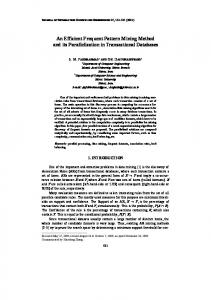
ECC design
An application for large polynomial multiplier is ECC. In this section we describe a simple ECC hardware accelerator design that applies the multiplier introduced in the previous sections. Figure 3 depicts the block diagram of the exemplary 233 bit ECC hardware accelerator. The ALU combines the functionalities of addition, squaring and allows bit manipulations. The ALU operations are performed within one clock cycle. The ALU requires 0.08mm2 silicon area in 0.25µm CMOS technology. The multiplier is one of the sequential IKMs, described in the previous section. Depending on the configuration it requires 3, 9, or 27 clock cycles. Corresponding to the speed the needed area is affected. It is not only the largest unit but also the most utilized one. The duty time is more than 90%.
Table 8: Results for an 233 ECPM on accelerator designs after synthesizing using different embedded polynomial multipliers. Mul Setup 233 8 233 4 233 2
5
Size [mm2 ] 0.90 1.02 1.36
Needed clk cycles 26999 9251 5344
Time [ms] 0.81 0.24 0.18
Energy [µWs] 25.1 12.8 10.6
Acknowledgment
Table 9: Comparison of GF (2m ) ECPM hardware designs. Ref our our [10] [3] [7] [9] [11] [15] [2]
Field GF(2163 ) GF(2163 ) GF(2163 ) GF(2163 ) GF(2167 ) GF(2191 ) GF(2163 ) GF(2191 ) GF(2233 )
Platform 0.25 µm ASIC Xilinx XC2VP70 0.13µm ASIC Xilinx XCV2000E Xilinx XCV400E Xilinx XCV3200E Xilinx XCV2000E 0.35 µm ASIC 0.13 µm ASIC
Time 0.08 0.11 0.19 0.14 0.21 0.06 0.05 6.21 6.68
Size 1.0mm2 , 35Kgates 5598 LUTs 117.5 Kgates 19508 LUTs 3002 LUTs ≈30000 LUTs 25763 LUTs 1.31mm2 71 Kgates
This work was partially funded by the German Ministry of Education and Research under grant 01AK060B and in part by EU under contract 26820.
References [1] Z. Dyka and P. Langendoerfer. Area efficient hardware implementation of elliptic curve cryptography by iteratively applying karatsuba’s method. In DATE, pages 70–75, 2005. [2] Elliptic semiconductor. CLP-22 Elliptic Curve Point Multiplier Core, 2006. Available from http://www.ellipticsemi.com/CLP-22 60102.pdf. [3] N. Gura, S. Shantz, H. Eberle, D. Finchelstein, S. Gupta, V. Gupta, and D. Stebila. An end-to-end systems approach to elliptic curve cryptography. In CHES ’02: Proceedings of the Second International Workshop on Cryptographic Hardware and Embedded Systems, 2002. [4] T. Itoh and S. Tsujii. A fast algorithm for computing multiplicative inverses in GF (2m ) using normal bases. Inf. Comput., 78(3):171–177, 1988. [5] A. Karatsuba and Y. Ofman. Multiplication of multidigit numbers on automata. Doklady Akademii nauk SSSR, 145:293–294, 1962. [6] J. L´opez and R. Dahab. Fast multiplication on elliptic curves over GF(2m ) without precomputation. In CHES ’99: Proceedings of the First International Workshop on Cryptographic Hardware and Embedded Systems, 1999. [7] G. Orlando and C. Paar. A high performance reconfigurable elliptic curve processor for GF (2m ). In CHES ’00: Proceedings of the Second International Workshop on Cryptographic Hardware and Embedded Systems, 2000. [8] F. Rodriguez-Henriquez and C. Koc. On fully parallel karatsuba multipliers for gf(2m ). In Proceedings of International Conference on Computer Science and Technology CST, 2003. [9] N. A. Saqib, F. Rodr´ıguez-Henr´ıquez, and A. D´ıaz-P´erez. A parallel architecture for fast computation of elliptic curve scalar multiplication over GF (2m ). In IPDPS, 2004. [10] A. Satoh and K. Takano. A scalable dual-field elliptic curve cryptographic processor. IEEE Trans. Comput., 52(4):449– 460, 2003. [11] C. Shu, K. Gaj, and T. A. El-Ghazawi. Low latency elliptic curve cryptography accelerators for nist curves over binary fields. In Proceedings of the 2005 IEEE International Conference on Field-Programmable Technology, FPT 2005. [12] Synopsys Inc. PrimePower: Full-Chip Dynamic Power Analysis for Multimillion-Gate Designs, 2005. Available from Synopsys website http://www.synopsys.com/products/power/primepower ds.pdf. [13] F. U.S. Department of Commerce/NIST. Digital Signature Standard (DSS), FIPS PUB 186-2, Jan. 27, 2000. [14] A. Weimerskirch and C. Paar. Generalizations of the karatsuba algorithm for polynomial multiplication. [15] J. Wolkerstorfer. Is elliptic-curve cryptography suitable to secure rfid tags? In Workshop on RFID and Light-Weight Crypto, 7 2005.
speed of our design but it is very small. With a LUT number of 3002, it requires about half of the area of our design on the FPGA. From our knowledge the fastest ECC design was reported in [11]. It requires merely 50 µs for a 163 bit ECPM, i.e. it is 40% faster than our design, but with its 25000 LUTs it is about five times larger than our implementation. In contrast, the ASIC design presented in [15] is a very small design. The ASIC manufactured in a 0.35 µm technology has a size of 1.31mm2 and supports two fields, but requires more than 6 ms for an ECPM. The energy consumption reported for this design is 213µWs for an ECPM in GF (2191 ), i.e. it is about the tenfold of our design. Another design that reports the power consumption is commercially offered on [2]. With this design a 233 bit ECPM requires 6 ms and a total energy of 140µWs for the 50 MHz design, manufactured as 0.13 µm ASIC. The comparison clearly indicates that our approach outperforms all other designs if area and processing time are taken into account. From our knowledge it is the most energy efficient that has been reported.
6
Conclusions
In this paper we have presented an ECC hardware design, that accelerates the ECPM for specific elliptic curves. the which we applied to B-233. The parameters of our design are very promising. Our design requires only 1.4mm2 cell area in a 0.25 µm technology and the calculation of a point multiplication takes less than 80 µs. The performance comparison clearly indicates that our approach outperforms most reported designs if area and processing time are taken into account. The good performance results from the very efficient core multiplier. It still requires nearly the half of the silicon area, is the performance bottleneck regarding clock cycles and clock frequency. However, this confirms that every improvement of the multiplier is a substantial contribution for the improvement of the whole EC hardware accelerator. Our hRAIK multiplication approach that has been proposed in this paper is such a contribution. It improves time, area, and power consumption of the polynomial multiplication and is therefore the cornerstone of the achieved ECC performance. 6