Architected Instruction Set from Yorktown) processor, an eight-issue ... Published in the Proceedings of ICCD'98, 5-7 October 1998 in Austin, Texas. Pesonal use ...
An Eight-Issue Tree-VLIW Processor for Dynamic Binary Translation Kemal Ebcioglu, Jason Fritts, Stephen Kosonocky, Michael Gschwind, Erik Altman, Krishnan Kailas, Terry Bright IBM T.J. Watson Research Center Yorktown Heights, NY 10598 Abstract Presented is an 8-issue tree-VLIW processor designed for efficient support of dynamic binary translation. This processor confronts two primary problems faced by VLIW architectures: binary compatibility and branch performance. Binary compatibility with existing architectures is achieved through dynamic binary translation which translates and schedules PowerPC instructions to take advantage of the available instruction level parallelism. Efficient branch performance is achieved through tree instructions that support multi-way path and branch selection within a single VLIW instruction. The processor architecture is described, along with design details of the branch unit, pipeline, register file and memory hierarchy, for a 0.25 micron standard-cell design. Performance simulations show that the simplicity of a VLIW architecture allows a wide-issue processor to operate at high frequencies.
1.0
Introduction
As the demand for increased performance in microprocessors continues, new architectures are required to meet this demand. Implementations of existing architectures are quickly reaching their limits as increases in current superscalar out-of-order issue are bounded by circuit complexity [1], and performance increases due to technology improvements are approaching their limits. A possible solution to these problems is the use of very long instruction word (VLIW) architectures, which do not have to deal with the complexity of having to re-arrange the instruction stream at execution time because they are statically scheduled to avoid dependency problems. Many previous VLIW architectures have suffered from problems that have limited their success in the general purpose computing market. These problems have included: poor performance on branch intensive code, and lack of binary compatibility. Previous studies have been performed on both branch intensive code and binary compatibility. Combining multiple control paths into a single predicated control path, such as with hyperblocks [2], or treegions [3], has shown excel-
lent performance improvement for branch intensive code. Binary compatibility studies have been successful in creating hardware and software methods for supporting compatibility both between different generations of VLIW processors [4][5][6][7], as well as between VLIW architectures and existing architectures [8][9]. This work presents the first full processor design that effectively deals with both problems. In this paper, we present the DAISY (Dynamically Architected Instruction Set from Yorktown) processor, an eight-issue VLIW processor using tree-based VLIW instructions [10] (also referred to as VLIWs) and just-intime compilation techniques. The processor was designed at IBM T.J. Watson Research Center using standard cell ASIC technology and currently simulates at 350 MHz. This paper is structured as follows: Section 2 shows how dynamic translation can be used to achieve binary compatibility with legacy instruction sets across a range of VLIW architectures. Section 3 describes DAISY, the target VLIW architecture based on tree VLIWs, and how it achieves high performance on control flow intensive programs. Section 4 outlines the processor core, including the branch unit, pipeline and register file. Section 5 describes details of the memory hierarchy. Section 6 discusses the layout and floorplan of DAISY, and Section 7 reports simulation results. Conclusions are presented in Section 8.
2.0
Dynamic Translation
While the performance advantages of VLIW architectures have always been acknowledged, binary compatibility between members of a VLIW family and also between VLIW architectures and existing architectures have been a major problem for the success of VLIW processors in the market place. To counter this problem, dynamic binary translation [8] is used to achieve 100% architectural compatibility between the DAISY VLIW architecture and the PowerPC architecture. Dynamic translation can also be used to provide compatibility with the Java Virtual Machine [11] and the IBM System/390 architecture.
Copyright 1998 IEEE. Published in the Proceedings of ICCD’98, 5-7 October 1998 in Austin, Texas. Pesonal use of this material is permitted. However, permission to reprint/republish this material for advertising or promotional purposes or for creating new collective works for resale or redistribution to servers or lists, or to reuse any copyrighted component of this work in other works, must be obtained from the IEEE. Contact: Manager, Copyrights and Permissions / IEEE Service Center / 445 Hoes Lane / P.O. Box 1331 / Piscataway, NJ 08855-1331, USA. Telephone: + Intl. 732-562-3966.
“Execute” PowerPC code
PowerPC Code Fragment
code already translated?
N
Y
Fetch VLIW Fragment
VLIW Code Fragment
VMM
Cache VLIW Fragment
Execute translated VLIW code
(Dynamic Translation)
Figure 1 - Dynamic translation of object code is performed as each code fragment is accessed for the first time. All future executions of this code are then executed in fast, native VLIW code. In the DAISY architecture, a system component called the virtual machine monitor (VMM) translates each fragment of code from the base architecture to the VLIW target architecture, as shown in Figure 1. The VMM works as follows: as each new fragment of code (such as a page) is executed for the first time, the code is translated to simple RISC-like primitives, scheduled in parallel to take full advantage of the available instruction level parallelism of VLIW architectures, and saved in a portion of main memory not visible to the old architecture. Subsequent executions of the same fragment do not require translation unless the fragment has been purged to reclaim space. DAISY includes new fast compiler algorithms for accomplishing the dynamic translation and parallelization across multiple paths and loop iteration boundaries [9].
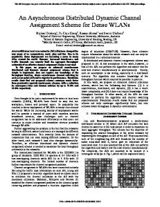
DAISY Processor
60X to PCI Bus Interface
L3 Cache
PCI Bus Flash ROM
VMM
Graphics
Ethernet
EISA Interface
2 shows a system level view of a PowerPC system based on the DAISY architecture.
3.0
The DAISY VLIW Architecture
The DAISY architecture defines a VLIW architecture designed for efficient binary translation of PowerPC code. Efficient binary translation is achieved through two mechanisms. The first is the tree structure of VLIW instructions which provides multi-way path and branch capability in every cycle. The second is the design of the instruction set which provides 100% compatibility with the base architecture through a set of simple RISC-like operations as well as the means to increase ILP through speculative execution, out-of-order loads, and other optimizations. The basic DAISY architecture is a load-store architecture with a 32-bit integer datapath and fixed-length 256-bit VLIW instructions. It provides 64 32-bit registers and 16 4bit condition registers. Each VLIW instruction contains 8 parallel three-operand operations and a control header containing information for control flow and predication. Future architecture revisions will include floating point.
3.1
Tree Structure
To achieve good performance on branch intensive code, each VLIW instruction implements a multi-way path selection scheme. Path selection proceeds by reading from the condition register file up to three conditions, which were the results of compares or condition operations in previous VLIWs. Testing these conditions, the multi-way path scheme can define up to four paths and branch targets per VLIW. The operations in each VLIW are predicated upon one or more paths of control flow so that only those operations along the selected path, known as the taken path, execute. Figure 3 gives an example of a tree-shaped VLIW instruction as implemented in DAISY.
Mouse EDO Translated Code DRAM
Keyboard
ccA
Figure 2 - The DAISY system architecture connects to a standard PowerPC system through the 60X interface. Shaded parts indicate the flash ROM storing the DAISY virtual machine monitor and the memory store for translated code.
P1
ccB L1 P4
ccC
L4
The DAISY emulation concept is different from other dynamic binary compilation strategies, where processbased emulation is supplied. In previous emulation strategies [12], emulation was a part of the operating system’s services. In the DAISY approach, the VMM is part of the firmware, and emulates the entire instruction set, including system level operations. As a result, the DAISY architecture is indistinguishable from a hardware implementation and can boot standard native operating system code. Figure
P2
P3 L2
L3
if ( ccA == false ) execute ops on path P1 branch to L1 else if ( ccB == true ) execute ops on path P4 branch to L4 else if ( ccC == false ) execute ops on path P2 branch to L2 else execute ops on path P3 branch to L3
Figure 3 - A tree VLIW instruction implements multiway selection of the tree-shaped paths of control flow. Operations within a VLIW are predicated upon the taken path, defined by the state of condition codes ccA, ccB, and ccC. The tree form, condition tests, branch targets and execu-
tion predicates for each VLIW are encoded in a 72-bit VLIW header, followed by 8 23-bit parcels, each encoding a three-operand operation. The VLIW header format allows any path through the VLIW instruction to specify what subset of the eight operations to execute if a particular path is chosen. These operations are defined by the DAISY instruction set.
3.2
Instruction Set
The DAISY instruction set supports normal integer operations including addition and subtraction, memory operations, compares, shifts, logic operations, and condition operations. In addition to these basic operations, there are a few compatibility operations for supporting efficient binary translation and emulation of PowerPC semantics, such as several commit operations for supporting speculative execution, load-verify operations for supporting out-of-order loads, and extender operations for providing additional operation functionality. Most operations can be executed in any issue slot, except for memory and extender operations, which may only be scheduled in four issue slots. For efficient binary translation support, the DAISY architecture contains a “load VLIW instruction address (LVIA)” operation. The LVIA operation loads the VLIW instructions corresponding to a section of PowerPC code. If the code is already translated and in memory, the LVIA operation returns the address of the appropriate VLIW starting instruction, otherwise it loads the VMM translator, which translates the PowerPC code before executing the corresponding VLIW instructions. The architecture provides speculative execution with precise exceptions using the support of a commit operation and register extender bits. Each register contains three extender bits: carry, overflow, and exception. While emulating PowerPC code, some of the registers in the DAISY processor correspond to the architected registers in a PowerPC (specifically, DAISY registers r0 through r31). When an operation is executed speculatively, it does not commit its results to the registers maintaining the emulated PowerPC state, but instead to the remaining DAISY registers. At the point in the emulated program when the PowerPC instruction is supposed to execute, a commit operation is used to copy the register contents to the emulated PowerPC destination register and change the state of the processor as specified by the extender bits. Aggressive reordering of memory references without memory disambiguation is also supported in the architecture. A load may be scheduled early and stored in a speculative register for use by other speculative operations before it is actually known if the value is correct. At the time in which the load was supposed to occur, a load-verify operation is scheduled. This load-verify performs the same load, then checks the result against the speculatively loaded value. If the values differ, an exception occurs.
Limited opcode space necessitated extender operations for some of the more specialized, less frequent operations. Using a pairwise organization of the ALUs (see floorplan in section 6), one ALU in a pair may use an extender operation to increase the functionality of an operation in the other ALU. This allows for longer immediate constants as well as addition and subtraction with carry. Special attention was given to memory operations for minimizing execution time. To enable single-cycle execution, memory operations were split into separate address generation and memory access operations. The address generation operation performs an address addition and saves the result in one of four dedicated memory address registers (MARs). In the next cycle, the load or store occurs using the address directly from one of the MARs. Like the extender operations, these two operations occur in paired ALUs. One ALU in the pair generates the address that is consumed by the other ALU for the memory access in the next cycle. This enables up to four memory accesses every cycle. Address translation in the TLB is logically identical to the PowerPC, implemented through a combination of hardware and software.
4.0
DAISY Hardware Design
A high performance hardware design has been developed for the target architecture described above. This design exhibits single-cycle execution of all operations, an aggressive high-speed memory hierarchy, full bypassing, and perfect multi-way branch performance, i.e., branching every cycle without branch prediction. The basic design shall be presented first, followed by a more detailed discussion of some of the hardware issues.
4.1
Processor Architecture
The basic processor architecture is an 8-issue VLIW engine, as seen in Figure 4. The register file is a unified 16read/8-write port register file with 64 32-bit registers. Similarly, the condition register file has 16 4-bit condition registers. It also has 8 write ports, but only requires 11 read ports: one for each issue slot and three for the branch unit. The branch unit decodes the tree VLIW header and determines the branch target and path of execution. The DAISY design uses an aggressive cache hierarchy to satisfy the large bandwidth requirements typical of VLIW architectures. There are separate L1 instruction and data caches, each providing single-cycle access. The L1 data cache is direct-mapped with 32 KB, while the L1 instruction cache is direct-mapped with 64 KB. Instructions and data are combined in the L2 cache, which is a directmapped 256 KB cache with a hit time of 4 cycles. Two interfaces provide access to a 16 MB off-chip L3 cache, and the 60X bus.
ALU ALU ALU ALU ALU ALU ALU ALU 0 1 2 3 4 5 6 7 L1 Data Cache 32 KB Branch Unit
L2 Cache 256 KB
L3 Interface
L3 Memory Interface
L1 Instruction Cache - 64 KB
60X Interface
60X Bus Interface
Figure 4 - Basic processor design
4.2
Branching
Providing efficient branch behavior was of primary importance in a hardware design of the DAISY architecture. Each VLIW instruction explicitly indicates all branch targets in its header, so the processor effectively branches every cycle. This design achieves perfect branch performance by splitting branch target selection into two phases. The first step in branching is to fetch all possible branch targets, enabling late selection of the desired branch target. Since fetching all possible branch targets from random locations in memory is too costly, the architecture requires the branch targets (up to 4) to be located consecutively in memory. As a result, the first branch phase fetches from the instruction cache a single block of memory containing all four possible branch targets. The address of this block, known as the Next Line Address, is contained in the previous VLIW, as shown in Figure 5. The second phase in branch evaluation is choosing the appropriate VLIW from among the block of four VLIWs. While a given VLIW instruction, VLIW n, is executing, its header is processed by the branch unit. The branch unit fetches up to three test conditions from the condition register file and evaluates the tree to determine the branch target and taken path. The branch target information selects the next VLIW for execution, VLIW n+1, from the block of four VLIWs. At the same time, the taken path information for VLIW n is fed to the execution unit which completes only those operations predicated upon the taken path. This two phase branching scheme provides perfect branch performance assuming the two branch phases occur in the first two stages of the pipeline. The first phase of branching, block VLIW fetch, must complete within the first stage to obtain the address for the next instruction fetch by the end of the cycle. The second phase of branching, tree VLIW header evaluation, must complete in the second stage to select the appropriate branch target from the block
4.3
Pipeline
Like the rest of the design, the pipeline of the DAISY processor was chosen for scheduling efficiency and achieving high ILP. It uses a three-stage pipeline for reducing scheduling constraints and branch penalties, while depending upon the simpler hardware design of VLIW architectures to achieving high frequencies. The three pipeline stages of the DAISY processor are Instruction Fetch, Execute, and Write Back, as shown in Figure 5. The stages have been carefully designed so that each has approximately the same delay. The instruction fetch (IF) stage begins by fetching the block of four target VLIW instructions from the specified address. A 4:1 multiplexer selects one of these VLIWs. The address, Next Line Address, in its header specifies the instruction fetch address for the next cycle. The VLIW is then latched at the end of the IF stage. IF
EX
Next Line Addr
WB Branch Unit
VLIW0 I-Cache Line
Register File - 64 GPRs, 16 CRs
of four VLIWs. The ability to branch every cycle without any misprediction penalty provides exceptional performance on control intensive code.
VLIW1 VLIW2 VLIW3
Operand Fetch
Execute
Figure 5 - Pipeline Stages The execute (EX) stage combines four major functions: branch evaluation, register fetch, bypassing, and execution. The stage begins with operand fetch, which fetches the register and condition register values, performs full bypassing of the 8 results from the previous VLIW, and selects between immediate and register sources. The operands are then sent to the branch and execute units. The branch unit evaluates the VLIW tree header and determines the branch target and taken path. Branch target selection indicates which of the four VLIWs in the IF cache line is selected for execution in the next cycle. Simultaneously, the execute stage receives the operands and executes all 8 operations, latching the results at the end of the EX stage. During the write back (WB) stage, the results of those operations predicated upon the taken path are committed and written back to the register files. Pipeline control is simple in the case of normal execution where the pipeline simply advances one stage each cycle, but requires special handling in the event of stalls or exceptions. During stalls and exceptions, the state of the pipeline must remained fixed until the stall or exception is handled. At high frequencies, because of the large wire delay
between units, it is not feasible to stop advancement of the pipeline in the same cycle the stall or exception event occurs. Instead, the processor core uses backup register to provide correct stall and exception handling. At the end of each normal cycle, the last pipeline state is stored into backup registers. When a stall or exception occurs, the current cycle completes, simultaneously writing an invalid state into the registers and the last valid state into the backup registers. On the next cycle the last valid state is restored from the backup registers. In subsequent stall or exception cycles, this state remains fixed. When the stall or exception completes and normal execution resumes, pipeline execution continues from the last valid state.
4.4
1024 L3 Cache (off-chip) 1024
Memory Hierarchy
Architectures employing high instruction level parallelism place a heavy burden on the memory hierarchy. Achieving maximum performance requires large fast multiported, single-cycle instruction and data caches. Figure 6 shows the top level memory hierarchy. The processor core is divided into four clusters of ALU pairs, each containing a load/store unit, a first level data cache port, a first level instruction cache port and a translation lookaside buffer (TLB) port. The first level instruction cache (I1 cache) is 64 KB, partitioned into four sections, each containing two operations for the attached cluster, along with duplicated control bits.
1024
1024
60X Interface
L2 Cache 256
Register File
The execute stage, which combines the register fetch and execute functions, is one of the critical paths in the DAISY processor. Since both of these functions are performed in a single cycle, register file read times are critical to cycle time. To minimize register read time, rather than a single register file with 16 read ports and 8 write ports, 8 identical copies of the register file with 2 read ports and 8 write ports per copy are used. Each execution unit fetches its operands from its own local copy of the register file, but writes its results to all 8 copies. This design trade-off minimizes the critical register read time of the execute stage at the expense of extra loading during register write back. However, write back time is not as critical because the whole WB cycle is dedicated to write back. Although combining the register fetch and execute functions into a single pipeline stage can be one of the limiting factors in achieving the fastest cycle time, this path is also balanced with other critical paths throughout the chip. Other such paths include the SRAM access and logic and wire delay for the first level instruction and data caches. Also, the combined execute stage allows the register fetch to occur in parallel with bypassing, effectively hiding the bypass delay. Full bypassing between all 8 issue slots is possible with only minimal impact on cycle time.
5.0
The first level data cache (D1 cache) is 32 KB. Two identical copies service the nearby ALU clusters. There are four identical copies of a 1K entry TLB, each with a single read and write port. The instruction and data caches are connected to an integrated 256 KB level 2 cache (L2 cache). A third level 16 MB cache (L3 cache), constructed using discrete off-chip SRAM devices, is attached to the L2 cache along with an integrated 60X interface.
256
256
I1cache_0 118
256
118
LD ST
256
I1cache_2
LD
ALU 0,1 cluster
ALU 4,5 cluster
ST
D1cache copy 0
D1cache copy 1
ST
cluster ALU 2,3
cluster ALU 6,7
LD
ST LD
118 I1cache_1 256
118 I1cache_3 256
Figure 6 - Top level memory hierarchy
5.1
I1 Cache
For the DAISY processor to achieve perfect multi-way branching on every cycle, single-cycle execution of the instruction fetch (IF) stage is critical. Wire delay is minimized by partitioning the I1 cache into four sections, which are each locally self-contained. Each partition services a single cluster of two ALUs, so the partition needs to hold only those portions of the VLIW instruction pertinent to that ALU pair. This includes two operations and information on the shape of the VLIW tree. Fast cycle time is achieved during the instruction fetch stage by replicating the branch unit at each cache partition. The VLIW tree header contained in each partition is used to perform address generation and branch target selection locally for each cluster. Implementing branching locally minimizes the wire delay for communicating the next instruction address to each cache partition. Figure 7 shows the details of an I1 cache partition. The I1 cache is direct mapped with 512 rows and four banks. Each line contains 4 VLIW instructions (1024 bits), one VLIW per bank, such that all four possible branch targets of the previous VLIW instruction reside in the same row
address (see section 4.2). The fetch address, Next Line Address, is applied to each bank in each partition, reading from the SRAM single-ported array bank one of the four VLIW instructions. Simultaneously, the I1 cache write buffers are examined for an address match. If a write buffer hit occurs, multiplexers select the write buffer outputs over the SRAM data. The data are then applied to a 4:1 multiplexer where a select signal from the branch unit selects the proper VLIW. On each access, the tag from the I1 directory is checked by a comparator and if a miss occurs, a stall signal is raised and an L2 request is made. When valid data comes from the L2, it is directly bypassed to the ALU clusters through multiplexers and simultaneously loaded into the write buffers, while the old contents of the write buffers are written into the SRAM array. WB0 L2data Bank0
I1_miss wb_hit or I1_miss L2data
WB1
Bank1
I1_miss
The D1 cache is direct mapped and has 32 byte lines. The implementation for multiple ports uses single-ported SRAM arrays organized into 8 banks. Data is interleaved on a 32 byte line basis, with lines 0,8,16,... in bank 0, lines 1,9,17,... in bank 1 and so on. All four requests can be satisfied in a single cycle when there are no bank conflicts. When multiple requests are made to the same bank, the VLIW stalls and the requests are prioritized by ALU number in left-to-right order. Use of 8 banks allows for faster array access times and reduces stalls from bank conflicts. Each read/write port maintains a separate copy of the D1 cache directory. On an access, TLB and D1 directory checks are performed. If the TLB directory does not match the upper bits of the effective address, a TLB miss exception occurs. Otherwise, if the real address coming out of the TLB matches the real address of the D1 directory, there is a D1 cache hit. A D1 cache miss is detected on the cycle after the SRAM or write buffer access, and the D1 cache stalls until valid data arrives from the L2 cache. The TLB is implemented as a direct mapped 1K entry array, which supports the usual PowerPC condition and protection modes, and additional information to support binary translation. Port3_data Port2_data Port1_data Port0_data
...
wb_hit or I1_miss L2data
WB2
...
...
Bank2
I1_miss wb_hit or I1_miss L2data
WB3
I1_miss
wb0_b0
wb1_b0
wb2_b0
wb3_b0
SRAM
addr0(27:30)
8:1
4:1
8:1
addr1(27:30)
hit0_sel
4:1
hit1_sel
Bank0
addr0(24:26)
...
...
8:1
8:1
Bank7 addr0(24:26)
...
Bank3
addr0(17:23) addr1(17:23) wb_addr(17:23) linefill_addr(17:23)
...
Addr_sel
...
...
8:1
8:1
L2data
addr1(24:26)
addr1(24:26)
addr0(27:30)
wb_hit or I1_miss
8:1
8:1
addr1(27:30)
2:1
subline_sel
NextLineAddr I1_data
2:1
d1_miss1 d1_miss0
byte_sel0 byte_sel1
2:1
2:1
Port0_dout Port1_dout
Figure 7 - I1 cache section Figure 8 - D1 cache dataflow for read operation
5.2
D1 Cache and TLB
Careful attention was given to the design of the D1 cache to support up to four memory operations per cycle. To effectively support such bandwidth, instead of a single D1 cache with 4 read ports and 4 write ports, two identical copies with 2 read ports and 4 write ports are used. As shown in Figure 6, each copy services a pair of ALU clusters. Using two copies decreases the wire delay and number of read ports, allowing for single-cycle loads, after address computation has been performed in a previous cycle. Each copy still requires four store ports to maintain a consistent view of the memory. However, store time is not as critical since write buffers hide the delay.
Each bank contains a 128x32 byte SRAM array, four 2x32 bit write buffers for stores and a 288 bit castout buffer. Figure 8 shows a diagram of the read path of the D1 cache. On a read, one of four addresses is selected by control logic for row selection and comparison with the addresses of previous stores in the write buffers. The 32 byte line read from the SRAM is multiplexed down to two 32 bit words, one for each port, while the data from the write buffers are similarly multiplexed to two 32 bit words according to the address comparisons. The eight words for each port from the banks are then multiplexed by bank select multiplexers. The desired data are finally selected according to the valid
L2 Cache
The L2 cache is logically seen as a unified 256 KB direct-mapped cache with 2 read ports and a single write port. One read port is dedicated for 128 byte wide I1 cache reads, while the other is for 32 byte wide D1 cache read and write accesses. Simultaneous I1 cache and D1 cache requests to the L2 cache are serialized. The L2 cache is implemented as a single one port, 2K row, 128 byte line SRAM array. Address selection logic arbitrates between access requests from the I1 and D1 interfaces. Data is read into two, 2:1 multiplexers, one of which allows the L3 data to be bypassed to the lower memory hierarchical levels, while the other is for castouts to the L3 cache. The 128 byte output of the first 2:1 multiplexer is then either used by the I1 cache or further multiplexed down to a 32 byte subline by the subline select logic for the D1 cache.
5.4
L3 Cache and 60X Interface
The L3 cache controller accepts a 128 byte request from the L2 cache and serializes the data into 32 byte wide bursts sent to four 32 byte wide off-chip SRAM banks. L3 misses and castout requests are sent to a simplified 60X interface unit, where a request is made for a 60X bus burst transaction of four 8 byte accesses to main memory. This design does not support cache snooping for multiprocessing, as only a uni-processor implementation is currently being considered. Multiprocessing support will be added in future implementations.
6.0
Chip Floorplan
Special attention was given to the layout of the processor for achieving maximum speed. Figure 9 shows a simplified diagram of the top level chip floorplan. The figure shows the placement of the multiple copies of the register files with relation to adjacent ALUs, the two D1 cache copies, and the four I1 cache partitions. Multiple branch unit copies are also shown adjacent to each I1 cache partition. Careful attention was paid to unit placement and duplication of units for minimizing wire delay between units. Design decisions to duplicate units were also balanced with limits for total chip area and logical cache sizes.
7.0
Results
The processor is implemented in VHDL for ASIC syn-
32KB L1 Data Cache copy 0
TLB copy 1
1/4 of 64KB L1 Inst. Cache
1/4 of 64KB L1 Inst. Cache
Branch Unit 0
Branch Unit 2
Reg File Reg File copy 0 copy 1
Reg File Reg File copy 4 copy 5
ALU 0
ALU 1
ALU 4
ALU 5
ALU 2 ALU 3 Reg File Reg File copy 2 copy 3
ALU 6 ALU 7 Reg File Reg File copy 6 copy 7
Branch Unit 1
Branch Unit 3
1/4 of 64KB L1 Inst. Cache
1/4 of 64KB L1 Inst. Cache
L3 Memory Interface Processor Core
TLB copy 2
32KB L1 Data Cache copy 1
1/2 of 256KB L2 Cache
5.3
TLB copy 0
1/2 of 256KB L2 Cache
byte data. Writes into the bank as a result of a store are done into the write buffers and marked valid after a TLB and directory hit. The write buffers also contain rotate logic, which performs byte rotations according to the store command. Path lengths are less critical for data stores, since the data is first written into the write buffer and is not dependent on SRAM access time.
TLB copy 3
60X Bus Interface Memory Hierarchy
Figure 9 - DAISY Processor Floorplan thesis into IBM’s 0.25µm SA-12 CMOS technology, with effective gate length of 0.18µm, 2.5V supply voltage and 5 wiring levels. The SRAM arrays are created with an array compiler, and the ALU and register file are created using bit-stacked standard-cell datapath circuits. Preliminary synthesis results show that the chip contains 486K complex logic gates and 478 KBytes of SRAM memory, within an area of 300 mm2. Initial critical path simulations of synthesized macros result in an estimated cycle time of 350MHz for nominal performance parts. VHDL simulations of the processor were performed with the aid of an assembler program, created to allow significant programs to be written in assembly and then translated to a binary memory image for driving the VHDL simulation. Architecture verification test programs were coded at the assembly level and executed on the VHDL model. System performance modeling was done using tracebased and execution-based simulators with the DAISY binary translator for the PowerPC architecture to explore various architectural trade-offs. The performance evaluations were done with these simulators using industry standard benchmarks. Results for page-based dynamic translation have been previously reported in [9]. More aggressive trace-based optimizations show promising results with higher levels of instruction level parallelism. Table 1 summarizes the performance estimates for tracebased binary translation on the machine described in this paper using SPECint95. The cycles per PowerPC instruction for each benchmark is broken down into components of: infinite cache performance, I-cache miss penalty, Dcache miss penalty, TLB miss penalty, and translation overhead. The cache hierarchy is flushed when a new fragment of code is translated, to reflect the adverse effect of translation events on the memory hierarchy. The actual translation overhead is low because the SPECint95 benchmarks have high code re-use rates. The degradation due to cache misses is quite significant in the present design, which follows a
simple stall-on-miss policy. But the cache penalty is likely to be reduced in future versions of the design, when more on-chip cache is available, and latency hiding techniques are used. Table 2 summarizes the simulation parameters. Benchmark
Inf CPI
I Cache
D Cache
compress gcc go ijpeg li m88ksim perl vortex
0.31 0.42 0.52 0.32 0.33 0.32 0.41 0.34 0.37
0.10 0.67 0.64 0.05 0.12 0.16 0.11 0.21 -
0.56 0.09 0.24 0.07 0.05 0.10 0.03 0.53 -
0.44
1.20
0.48
SPECint95
D TLB
translation
0.02 0.00 0.00 0.02 0.00 0.00 0.00 0.09 -
0.00 0.02 0.00 0.00 0.00 0.00 0.00 0.00 -
Tot. CPI
0.99 1.20 1.40 0.46 0.50 0.58 0.55 1.17 0.78
(geom mean)
TPC-C
0.16
0.00
2.28
Table 1 ILP performance given as cycles / PowerPC instruction - the translation cost is based on a 4000 cycle per translated PowerPC instruction cost. cache TLB I1 D1 L2 L3 memory (60X)
size
assoc.
line size
1K entry 64 KB 32 KB 256 KB 16 MB -
1
-
1 1 1 1 -
128 byte 32 byte 128 byte 128 byte -
latency (cycles) 1 hit, 41miss 1 1 4 18 106
Table 2 Memory hierarchy used for performance simulations - the cycle latency specified for data accesses excludes address generation which is performed separately
8.0
Conclusion
Described was an 8-issue, tree VLIW processor which uses dynamic translation for binary compatibility with existing architectures. The architecture uses tree-based VLIW instructions providing multi-way path and branch selection for improved performance on branch intensive code. Eight ALU operations may be scheduled per VLIW with support provided for speculative execution. The architecture allows up to four load/store operations per VLIW to satisfy the bandwidth requirements of high instruction level parallelism architectures. The hardware design uses a three-stage pipeline which provides single-cycle execution of all operations and per-
fect multi-way branching every cycle. An aggressive memory hierarchy is necessary to supply the four simultaneous load/store operations per VLIW. Numerous redundant circuits decrease loading and wire delay for high frequency operation. A VHDL ASIC design was simulated and synthesized. Preliminary results indicate exceptional processor speeds are achievable even in ASIC technology, with increased performance easily realizable in a custom implementation.
9.0
References
[1] S. Palacharia, N.P. Jouppi, and J.E. Smith, “Complexity-Effective Superscalar Processors”, Proc. of the 24th International Symposium on Computer Architecture, Denver, CO, June 1997. [2] S.A. Mahlke, D.C. Lin, W.Y. Chen, R.E. Hank, and R.A. Bringmann, “Effective Compiler Support for Predicated Execution Using the Hyperblock”, Proc. of the 25th International Symposium on Microarchitecture, pp. 45-54, Portland, OR, December 1992. [3] S. Banerjia, W.A. Havanki, and T.M. Conte, “Treegion scheduling for highly parallel processors”, Proc. of the 3rd International Euro-Par Conference, pp. 1074-1078, Passau, Germany, August 1997. [4] J.H. Moreno, M. Moudgill, K. Ebcioglu, E. Altman, B. Hall, R. Miranda, S.K. Chen, and A. Polyak, “Architecture, compiler and simulation of a tree-based VLIW processor”, IBM Journal of Research and Development, Vol. 41, No. 3, pp. 287-302, May 1997. [5] T.M. Conte and S.W. Sathaye, “Dynamic rescheduling: A technique for object code compatibility in VLIW architectures”, Proc. of the 28th International Symposium on Microarchitecture, Ann Arbor, MI, November 1995. [6] B.R. Rau, “Dynamically scheduled VLIW processors”, Proc. of the 26th International Symposium on Microarchitecture, Austin, TX, December 1993. [7] J.H.Moreno, K. Ebcioglu, M. Moudgill, and D. Luick, “ForestaPC User Instruction Set Architecture”, IBM Research Report RC20733, Yorktown Heights, NY, February 1997. [8] P. Emma, “Method and Apparatus for the Transparent Emulation of an Existing Instruction-set Architecture by an Arbitrary Instruction-set Architecture”, U.S. Patent No. 5619556, April 1997. [9] K. Ebcioglu and E. Altman, “DAISY: Dynamic compilation for 100% architectural compatibility”, Proc. of the 24th International Symposium on Computer Architecture, pp. 26-37, Denver, CO, June 1997. [10] K. Ebcioglu, “Some Design Ideas for a VLIW Architecture for Sequential Natured Software”, in M. Cosnard et al.(eds.), Parallel Processing (Proceedings of IFIP WG 10.3 Working Conference on Parallel Processing), pp. 3-21, North Holland, 1988. [11] K. Ebcioglu, E. Altman, and E. Hokenek, “A JAVA ILP Machine Based on Fast Dynamic Compilation”, International Workshop on Security and Efficiency Aspects of Java, Eilat, Israel, January 1997. [12] N. Rubin and A. Chernof, “Digital FX!32: A Utility for Fast Transparent Execution of Win32 x86 Applications on Alpha NT”, Hot Chips IX, Palo Alto, CA. August 1997. [13] ASIC SA-12 Databook, International Business Machines, IBM Microelectronics Division, Hopewell Junction, NY, June 1997.