picts a simpli ed view of an FPGA chip. The chip has a rectangular array of identical slots, called Programmable logic cells (PLCs). The input circuit needs to be ...
An Empirical Model For Accurate Estimation of Routing Delay in FPGAs� Tanay Karnik
and
Sung-Mo Kang
Coordinated Science Laboratory, 1308 W. Main St., University of Illinois, Urbana, IL 61801.
Abstract
We present an empirical routing delay model for estimating interconnection delays in FPGAs. We assume that the routing delay is a function of interPLC distances, circuit size, fanout of the net and routing congestion in the channel. We performed extensive simulations of various circuits to generate a su�ciently large dataset. Our method estimates delays by reading the average value tables and interpolating the values, if necessary. We present a rigorous statistical justi cation of this delay model. Our results show that our method predicts the delays within 20% of actual and it far outperforms all other existing techniques.
1 Introduction
In VLSI technology the interconnection area has become a more important factor in the total chip size than the cell area. Minimizing interconnection length minimizes the interconnection delay which leads to low power consumption. During physical layout synthesis, actual interconnection lines are determined at the routing stage. A fast interconnection length estimation technique is needed to help the synthesis stages before routing. Figure 1 depicts a simpli ed view of an FPGA chip. The chip has a rectangular array of identical slots, called Programmable logic cells (PLCs). The input circuit needs to be mapped onto the slot array. Intra-chip routing resources are shown as inter-slot routing lines and switches. Lines are of variable lengths and switches exist at each crossing. Direct extension of the conventional delay estimation algorithms to FPGAs is ine�cient [1]. The routing resources are limited and predetermined. The transistor sizes, pins on the chip, number of I/Os of PLCs, logic delays and the channel widths cannot be varied. Hence timing speci cations of the chip are mainly controlled by interconnect. Most of the previous approaches [1, 2, 3, 4, 5] have simpli ed the estimation problem by calculating Elmore function of the Manhattan distance or the semiperimeter length of the net under consideration. Switches are ignored. Our experiments showed that length and delay do not have a simple relation. In [6], the authors attempted to generate a more realistic model of FPGA routing delay
� This research was supported in part by the Joint Services Electronics Program (JSEP) under contract N00014-94-J-1270 and AT&T Bell Laboratories.
Switches
Slots
I/O Pins Inter-Slot Routing Lines
Figure 1: Simpli ed FPGA Chip as a piecewise approximation function of wire length. We assume that the routing delay is a function of horizontal and vertical distances between PLCs, circuit size, fanout of the net, and routing congestion around the net. Our model is empirical and accurate for predicting actual delay values, and it performs even better for comparing two solutions. The rest of the paper is organized as follows. Next section describes the chip speci cations and the routing delay model. We provide statistical validation in section 3. This is followed by the results of prediction in section 4. Section 5 concludes the paper.
2 Routing Delay Model
Our empirical model is derived from actual delay values. These delay values were generated using AT&T's ORCA1 Development System (ODS) [7]. The FPGA chip for our experiments is assumed to be ATT1C05 [8]. The chip has a nibble-oriented architecture with 12 � 12 slot-array, 5000 usable gates, 576 latches and 192 user I/Os. Each PLC has 19 external inputs and 6 outputs. It has four 64-bit look-up tables (LUT) and 4 ip ops (FF). The routing resources are of variable lengths and have three types in our FPGA chip. First type of lines (called X1) span one slot, second (called X4) span four slots and the third (called XL) span the entire width or height of the chip. Both the line and switch parasitics contribute to the routing delay. We explain some notations before explaining the delay model:
An FPGA chip has � available PLC slots. A slot �ij is a possible cell position at ith row and j th column. A cell C corresponds to a PLC. Each cell has I/O delays �C and nets NC . An I/O delay �ij from cell i to cell j is associated with a routing connection. 1 Optimized Recon gurable Cell Array
Hd
TPLC1
I Vd O
6
Delay
TPLC2
4 10 2 7.5
0 2.5
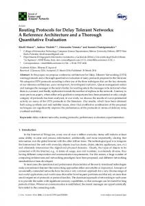
Figure 2: Intrachip Routing Delay
= F (Hd; Vd ; S; FN� ; �� ) where, Hd is the horizontal distance, Vd is the vertical distance, S is the circuit size, fN� is the fanout of the net (N� ) and �� is the routing congestion around �. The model is developed for a particular chip, but our method of model generation can be easily extended to other FPGA chips. Similar experiments can be performed for various other FPGA architectures supported with synthesis tools. The model does not have to include chipdependent variables, but there are other circuit-speci c synthesis-dependent variables, such as number of I/Os, PLC orientation, distance to fast routing lines, etc. It is very di�cult to explore benchmark circuits with su�cient variance in values of these variables. Our model provides accurate results without considering these variables. Hence they may be statistically dependent on the variables we have already taken into consideration. We explain the explored variables in our formulation: InterPLC Distance: As Hd and Vd each vary from 0 to 11 for a node, the required routing resources vary. However, the delay is not directly proportional to these variables. Please refer to the surface plot in gure 3. We chose a circuit with 2 PLCs connected by one node. The two PLCs were placed at all possible positions on the chip. As the chip is almost unoccupied and there is only one fanout line, the variables a�ecting the routing delay are Hd and Vd only. The delay of the node does not increase linearly with Hd and Vd . A node spanning three slots involves three X1 lines and spanning four slots utilizes one X4 line. As there are less switches in one X4 line than three X1 lines, the routing delay is less for the four-slot node than a three-slot node. Thus, we cannot characterize the routing delay as a simple function of these distances. The reason for use of these two variables instead of a combined variable as Manhattan distance measure (Hd + Vd ) is also evident from the gure. The surface plot is symmetric across x = y line which means Hd and Vd can be interchanged. However, the plot does not show constant values on x + y = Const lines. That clearly indicates that Man��
2.5 10
8.0
8.0
H=5,V=9,F=2,R=25 H=7,V=2,F=4,R=25
6.0
H=1,V=8,F=3,R=25
4.0
H=0,V=3,F=1,R=25 2.0
1
2
3
Circuit Size Category
4
6.0
H=5,V=10,S=72,R=25
Average Routing Delay
10.0
Average Routing Delay
We assume intrachip routing delay of a node � as a following function as shown in Figure 2:
Vd
7.5
Figure 3: Intrachip Delay Table Tiny1 Average Routing Delay
A net N is characterized by its source cells SRC N and its destination cells DST N . A node � corresponds to a net N� from source SRC � to destination DST � . A net can have multiple nodes associated with it, but a node is associated with just one net.
5 5
Hd
H=6,V=2,S=98,R=25 6.0
H=3,V=7,S=10,R=25
4.0
H=0,V=2,S=40,R=25 2.0
1
2
3
Fanout
4
5
5.0 H=3,V=2,S=40,F=4 H=0,V=6,S=10,F=5 4.0 H=2,V=0,S=72,F=3
H=1,V=1,S=98,F=1
3.0
2.0 20.0
40.0
60.0
80.0
Maximum Congestion
100.0
Figure 4: Delay versus Size, Fanout and Congestion hattan distance or semiperimetric measures should not be calculated for estimating intrachip routing delay for FPGA chips. Circuit Size: As the size of the circuit grows, the routing requirements grow. In fact it is quite possible that all nodes in the circuit mapped on more than 120 PLCs (out of total 144) may not be routable on ATT1C05. Figure 4 shows sample average delay values plotted against various circuit size categories. Due to various design styles and application requirements, the circuits with the same size have di�ering routing requirements. This prohibits the delay to be a closed-form function of circuit size. Fanout: The placement of cells connecting a large fanout net is very crucial for its subsequent routing. If these cells are placed away from each other, the resulting circuit may not be even routable. Due to xed routing resources, some of the fanout lines may take an indirect longer path than direct Manhattan line. Figure 4 depicts the e�ect of varying fanout on routing delay. Hence we include fanout as a variable in our routing delay model. Routing Congestion: The most di�cult variable to analyze is routing congestion around a node. The values of circuit size and fanout are available before synthesis begins. Routing congestion is the most routing-dependent variable in our model. There is no simple metric to evaluate congestion. As this variable cannot be evaluated, the relation of routing delay to this variable is di�cult to formulate. It is impossible to de ne an accurate analytical expression. Let �O be occupied slots in bounding box of size �� corresponding to �. We de ne routing congestion as: � = ��O� � 100 Figure 4 shows the variance of routing delay versus �. The erratic behavior of this variable can be clearly seen in the gure. Furthermore, the variation in routing delay is
less than that due to other variables. Hence we have empirically determined and included a congestion multiplier as follows:
8> 1:0 < 1:1 �m = >: 1:2 1:3
if 0 < �� � 25 if 25 < �� � 50 if 50 < �� � 75 if 75 < �� � 100
2.1 Empirical Model Generation
None of the variables has a direct relation with routing delay. All the above mentioned problems led us to design an empirical model for intrachip routing delay. To avoid over tting errors, we do not generate delay models for large circuits. We performed preliminary experiments to determine the routing delay variation according to circuit size and determined following 5 categories: Tiny Small Medium Big Large
if if if if if
1 5 21 55 91
� � � � �
S S S S S
< < <