An Implementation Comparison of an IDEA Encryption Cryptosystem on Two General-Purpose Reconfigurable Computers Allen Michalski1, Kris Gaj1, Tarek El-Ghazawi2 1
ECE Department, George Mason University 4400 University Drive, Fairfax, VA 22030, U.S.A. 2 ECE Department, The George Washington University 801 22nd Street NW, Washington DC 20052, U.S.A. {emichals, kgaj}@gmu.edu,
[email protected] Abstract. The combination of traditional microprocessors and Field Programmable Gate Arrays (FPGAs) is developing as a future platform for intensive computational computing, combining the best aspects of traditional microprocessor front-end development with the reconfigurability of FPGAs for computation-intensive problems. Several prototype PC-FPGA machines have demonstrated significant speedups compared to standalone PC workstations for computationally intensive problems. Cryptographic applications are a clear candidate for this type of platform, due to their computational intensity and long operand lengths. In this paper, we demonstrate an efficient implementation of IDEA encryption, using two of the leading reconfigurable computers available, SRC Computers’ SRC-6E and Star Bridge Systems’ HC-36. We compare the hardware architecture and programming model of these reconfigurable computers, and the implementation of a common IDEA encryption architecture in both platforms. Detailed analyses of FPGA resource utilization for both systems, data transfer and reconfiguration overheads for the SRC system, and a comparison between SRC and a public domain software implementation are given in the paper.
1. Introduction The need for faster computational processing methods has grown along with the desire to process large amounts of data in shorter periods of time. Approaches to this problem have typically involved microprocessor-based solution, utilizing concurrent processing with multiple processors within a single machine or in a cluster of workstations over a network. Since their introduction, FPGAs have emerged as a low cost complement to traditional microprocessor software and hardware solutions for computationally intensive applications, due to their hardware reconfigurability [1]. Several workstation-based FPGA systems are available today for commercial applications. These “reconfigurable computers” make use of workstation microprocessor(s) for front-end processing, and provide one or more FPGAs for computations less suited for a microprocessor. The choice of how a design can be divided between a microprocessor and an FPGA depends on the development environment available for the system. In this paper, we explore the efficient implementation of pipelined IDEA encryption within two such available reconfigurable computers: the SRC-6E from SRC Computers, and the HC-36 from Star Bridge Systems. This paper discusses the hardware architectures and development tools of both systems in detail, and provides FPGA timing and utilization results for both systems. A summary including the state of development of both systems is also presented.
2. FPGAs and Reconfigurable Computing An FPGA is a regular structure of basic modules called Configurable Logic Blocks (CLBs), which can be interconnected to provide hardware implementations of algorithms required by a designer. FPGA interconnects between modules are under the designer’s complete control [2]. The FPGAs used in both the SRC and Star Bridge systems are the Xilinx Virtex II 6000 series, which have a capacity of six million system gates, and provides dedicated logic for fast carry propagation for addition operations, multipliers that handle operand sizes up to 18 bits, and block RAMs for local memory access. FPGAs are reconfigurable, meaning that the FPGA device can be configured to carry out a specific function, and can be reconfigured to carry out a different function at a later time. The term “reconfigurable computing” is used to describe a combination of microprocessor systems with FPGAs to provide a reconfigurable hardware environment. Both the SRC and Star Bridge systems are
examples of reconfigurable computing platforms. Reconfigurable computers offer benefits over microprocessor-based hardware solutions because FPGAs can more easily exploit computational precision and operand sizes required by the design, and can implement operation pipelining and parallelism specific to the needs of the application being developed. Microprocessor instruction sets have fixed operand lengths that may not match operand sizes specific to the design, and the implementation of algorithms typically involves multiple-instruction executions for one algorithmic operation. In addition, much of the microprocessor’s capability is unutilized, since a general-purpose microprocessor is designed to implement a wide variety of operations specific to a workstation computing environment, whereas most design requirements for cryptographic systems only use a subset of the full capabilities of a microprocessor. All of the resources of an FPGA can be dedicated to the needs of a design, which provides a more efficient implementation versus a single or multi-processor-based design solution.
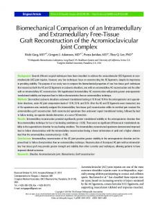
3. The SRC-6E 3.1 SRC-6E Hardware Overview The SRC-6E system architecture frontend consists of two dual Intel processor motherboards. Each motherboard contains two Intel P3 Xeon processors and 1.5 GB of memory. Each system hosts a multi-processor version of the Linux operating system, and provides two distinct Linux-based microprocessor-FPGA reconfigurable computers. An SRC MAP® processor is attached to each Intel motherboard, as shown in Fig. 1. Each MAP processor consists of two Xilinx Virtex II 6000 FPGA chips available for user logic, and a control Fig. 1. SRC-6E Hardware Architecture processor, which is also a Xilinx Virtex II 6000 FPGA, all running at a clock rate of 100 MHz. The control processor implements fixed control logic, and is responsible for direct memory access (DMA) transfers between Intel system memory and the onboard memory of the MAP processor. The user logic and control FPGAs have access to six banks of dual port 512k x 64 bit static RAM providing a total of 24MB of memory external to the FPGAs. The MAP control processor communicates with the Intel processors through a SNAP interconnect. The SNAP interconnect is a high speed, low latency interface which functions as a Double Data Rate (DDR) memory interface, and plugs into a DDR SDRAM slot on the motherboard. SNAP provides higher data throughput between the Intel processor and the MAP processor versus component interfacing using the PCI-X bus. 3.2 SRC-6E Programming Environment SRC has created a development environment that uses traditional programming paradigms in addition to hardware description language (HDL) development for implementing a design with the MAP FPGAs, as shown in Fig. 2. The SRC environment provides the ability to implement FPGA user logic using either C or FORTRAN sourcecode alone, or in combination with HDL sourcecode. GNU compilers are provided for C or FORTRAN sources that target the Intel processors, and SRC provides its own C or FORTRAN compilers that target the MAP processors. The MAP processor compilers produce Verilog code which is then synthesized using Synplify Pro, and Xilinx tools perform map, place and route. The GNU compilers allow the use of ANSI-compliant C or FORTRAN code and libraries, which allows for integration with other existing UNIX applications. The design environment is hosted in each Linux platform within the SRC-6E. The compilation process consists of compilation of user logic HDL files, if present, that will execute on the MAP processor, compilation of C or FORTRAN code that will also execute on the MAP processor, and compilation of the C or FORTRAN code that will execute on the Intel processors. The compilation process places wrapper code around logic that resides within the FPGAs to facilitate data transfer and control synchronization between the microprocessor and MAP processor. The binary files produced by each compile process are combined into one single executable for the host Intel platform, which is responsible for loading the Intel and MAP processors with the code compiled for each.
2
3.3 Designing within the SRC-6E Designs in SRC can have required operations performed on either the Intel or MAP processors. Within the MAP processor, FPGA designs can be implemented using a C or FORTRAN source alone, a C or FORTRAN source in combination with HDL, or completely in HDL, using a C or FORTRAN source to provide data transfer services. A simple API is available in the high-level language (HLL) to provide control functionality and data transfer functions between the Fig. 2. Overview of the SRC Compilation Process Intel and MAP processors, and the passing of data to and from included user HDL designs. MAP C sourcecode data types are limited to 32 and 64 bit types. HDL source that is targeted for the MAP processor is called a macro. SRC supports either VHDL or Verilog sources within macros. A macro’s primary characteristics are defined as functional, stateful, or external. Additional characteristics define latency of the design and whether the design is pipelined. An “info” file is used to describe these characteristics. A functional macro is one that carries no state information, and therefore doesn’t require the reset of a state machine. A stateful macro is one that caries state information and may need to be reset during a data cycle. An external macro is one that needs direct hardware access to memory, versus using HLL calls to read memory and supply data to the design. Latency defines how many clock cycles are needed before a result is available, and the pipeline attribute defines whether the macro can take data on each clock cycle. The combination of all these attributes defines the HDL macro supplied by the user. If a C or FORTRAN source is used alone or in combination with HDL source to implement the design within the MAP processor, the compiler attempts to extract the maximum parallelism from the code and generate pipelined hardware logic for instantiation in the MAP FPGAs [3]. 3.4 Debugging within the SRC-6E Debugging within SRC can be attained by traditional functional testing of HDL outside of SRC and traditional HLL debugging techniques, or using SRCs MAP debugger. The MAP debugger provides hardware debugging of code compiled for the MAP processor, and emulation debugging of emulation or simulation code. Emulation is based on specially formatted “data flow graph” C routines, provided by the compiler from existing HLL source if that is used to implement logic, or by the user in an additional file if HDL is also used, that emulates the functionality of the design being implemented in the MAP processor. Simulation mode actually simulates the HDL produced by the compiler, which requires a license for a Verilog simulator not included in the development environment.
4. The Star Bridge HC-36 4.1 HC-36 Hardware Overview The Star Bridge HC-36a consists of a Tyan S2720 dual Intel P4 Xeon processor motherboard with 4 GB of memory. Attached to the motherboard through the PCI-X bus is a PCI card containing two Virtex II 4000 FPGAs for dedicated PCI and hardware control, one Virtex II 6000 FPGA allocated for user-designed FPGA control functions, and 4 Virtex II 6000 FPGAs available for user logic, as shown in Fig. 3. FPGA clocks are set to the PCI-X clock speed, with the FPGA digital clock manager used to provide clock speeds other than the PCI-X clock speed. Star Bridge uses the name “HyperComputer®” to refer to this combination of FPGAs, an Intel-based frontend, and Star Bridge’s VIVA development environment [4]. The environment is hosted in Microsoft’s Windows 2000 Server operating system.
3
FPGAs available for user logic are referred to as PE1 to PE4. These four PEs (Processing Elements) have dedicated 50-bit connections to each other. Each PE, along with the XPoint FPGA mentioned below, has four banks of memory, each bank having 512 MB of RAM with a 64-bit PE interface. This gives a total of 10 GB of memory with 20 64-bit independent memory channels within the user FPGAs. Control FPGAs available to the user consist of an FPGA known as XPoint and a router FPGA. XPoint connects to the four user FPGAs using dedicated 32-bit data connections, and is allocated to provide user-defined control interfacing to the user FPGAs. The router FPGA has dedicated 94Fig. 3. Star Bridge HyperComputer FPGA Configuration bit connectivity to the user FPGAs, and provides additional user FPGA connectivity. The base grouping of four PEs is called a Quad Element. Only one Quad Element is available in the HC-36a, however each XPoint control FPGA can be used to control two Quad Elements. This structure of one XPoint control FPGA along with two Quad Elements can be replicated to create larger FPGA arrays, and is used to create larger Star Bridge platforms [4]. 4.2 The Star Bridge Programming Environment VIVA® is Star Bridge’s proprietary development environment. It provides a graphical user interface based on “drag and drop” design principles. VIVA’s design language, “Implementation Independent Algorithm Description Language” or IIADL, is object-based and uses object attributes to specify different options within the design. Fig. 4 shows the VIVA Integrated Development environment (IDE). Designs within VIVA can be allocated to execute on either the Intel platform or the FPGA array. Objects that execute on the Intel processor are implemented using pre-built VIVA libraries within Windows. VIVA is able to use Windows COM (Component Object Model) to communicate with other Windows applications, allowing Windows applications that make use of COM methods to be integrated in with VIVA FPGA designs. VIVA provides its own proprietary synthesis tool for designs that will run on user FPGAs. The target of the synthesis tool is defined by a system description. VIVA includes system descriptions for the Pentium x86, which allows simulation of the design in an x86, and for specific PEs in the FPGA array. VIVA’s system descriptions allow VIVA to abstract out the target hardware description from the design to be implemented, allowing VIVA to target hardware other than its own. If the design is targeted for a PE, the synthesis EDIF output is fed into Xilinx place and route tools to produce a final binary, which VIVA then loads onto the Intel processors and the FPGA array. After initial execution, the VIVA binary can be saved in a file format that can be loaded using VIVA command-line tools or within the VIVA development environment. 4.3 Designing within VIVA VIVA defines basic data types, from which objects can be built. The basic types are Bit, Variant, Vector, NULL, LSB, MSB and BIN. Bit is the only non-abstract fundamental data set. Within VIVA, data sets are basically recursive combinations of Bits. Each type therefore has two basic objects associated with it: an Exposer and a Collector. A data set Exposer takes the data set and outputs its two children data sets. A collector does the opposite: it takes two child data sets and combines them into one parent data set. For instance, a BIN016 (16-bit binary) data set, when exposed, will produce two BIN008 (8-bit binary) data sets. A MSB016, when Exposed, will produce a MSB001 and a MSB015. This is equivalent to splitting out the most-significant bit of a std_logic_vector(15 downto 0), and returning a std_logic and a std_logic_vector(14 downto 0).
4
The above definition of types allows for recursion of large data sets into small data sets, which is useful when a large operation is comprised of smaller operations of the same type. For instance, a 16-bit AND gate can be built using a tree of 2-bit AND gates, which can be built recursively. In order for recursion of an operation to be properly implemented, two objects for the operation must be created: a base object of the smallest acceptable operand size, and a recursive version of the object, which tells VIVA how to recurse down to the base operand object. Operands can be overloaded by simply copying the operand object design and changing the input data types, effectively overloading the operand type to handle different data sets. Objects can incorporate other types of objects, which allows for the hierarchical building of basic objects. VIVA provides basic operands such as AND, OR, and INVERT, which are standard to VIVA. These basic objects can be implemented in multiple system descriptions. VIVA objects, in general, can be designed to be implemented in multiple system descriptions or in a specific system description only. VIVA provides a library of additional operands, and data types built from the standard data types. This library, Corelib, has objects ranging from registers through state machines used for design control to file I/O objects for data transfer from and to a Windows file (see Fig. 4). This library is meant to be the basis for designs built in VIVA. 4.4 Debugging within VIVA Debugging a design within VIVA is performed by loading the x86 system description into a design simulate design components within the x86 environment. There is no in-place hardware debugger, although one is planned for future release. The simplest method of input and output testing is displaying inputs and outputs using widgets, which can be displayed using scrollbars, textboxes, graphics, and a number of other selections, as in Fig. 4. The clock can be manually single-stepped or continuously run. Windows COM objects can be integrated in to provide advanced debugging of the data output of a design.
5. IDEA 5.1 The IDEA Algorithm
Fig. 4. VIVA Synthesis Output using the X86 System
The International Data Encryption Algorithm (IDEA) is a symmetric block cipher developed by Xuejia Lai and James Massey of the Swiss Federal Institute of Technology and published in 1990[5]. At that time it was suggested as a candidate to replace DES, however its widest adoption has been in PGP, which has insured widespread use of the algorithm. IDEA uses a 128-bit key to encrypt data blocks of 64 bits. IDEA consists of eight rounds follow by a Transformation half-round that provides a 64-bit encrypted output. A round consists of a Transformation half-round and a Mangler half-round, of which an excellent description is provided by William Stallings in the book “Cryptography and Network Security: Principles and Practice” [6]. IDEA makes use of three basic operations to carry out encryption and decryption: a 16-bit XOR operation, a 16-bit modulo addition operation (mod 216), and a 16-bit modulo multiplication operation (mod 216 + 1). In addition, an all-zero operand input to a modulo multiplier within IDEA equals 216 for internal calculations. Each round requires six keys: four for the Transformation half-round and two for the Mangler halfround. For the total 8.5 rounds required for IDEA encryption, 52 16-bit keys are required. The first eight keys are provided by the input key. Each additional set of eight keys is generated by performing a circular left shift of 25 bits of the previous eight key set. 5.2 A Common Design Choice for IDEA Implementation within SRC and Star Bridge The XOR and modulo addition operations of IDEA can be easily implemented. The most difficult operation, multiplication mod (216 + 1) with the input of 0 = 216, can be broken down into three cases:
5
multiplication of two nonzero inputs, multiplication where one input is zero and multiplication where both inputs are zero. For multiplication of two nonzero numbers, the following rule is used [6]: ab mod(2n + 1) = (ab mod 2n) - (ab div 2n) if (ab mod 2n) (ab div 2n) ab mod(2n + 1) = (ab mod 2n) - (ab div 2n) + 2n + 1 if (ab mod 2n) (ab div 2n) For the remaining two cases, zero tests are used to mux in appropriate nonzero results and constants to provide the correct answer. To minimize latency, the use of a Virtex II hardware multiplier was desired to implement the two equations above. Since a 16x16 multiply operation using a single Virtex II 6000 block multiplier requires over 10 ns, a two-level three pipeline “divideand-conquer” strategy was used to meet the 10 ns timing constraint. This method requires four 8x8 multiplies along with column additions [7]. Design choices for IDEA centered on making each half-round modular to create a repetitive instantiation, therefore key scheduling is broken into a unit that can be implemented in a modular round. The solution for key scheduling requires the generation of six keys for each round. After eight keys have been consumed, though, a 25-bit rotate left operation is Fig. 5. IDEA Block Diagram required. To accommodate the above two constraints, a unique constant is input to each round’s key scheduler, which selects a mux that determines where the key rotate operation occurs within that round, if required. The design was pipelined in order to achieve high throughput. Both data and key scheduling were pipelined, which allows this core to be used in IDEA breaking or encryption since different data blocks can be introduced with either the same or a different key at each clock cycle. Pipeline placement was chosen based on synthesized VHDL and Xilinx place and route results for a target Xilinx II 6000 FPGA and a timing constraint of 10 ns (100 MHz). The final design has a pipeline latency of 116 clocks: each Transformation half-round requires four clock cycles and each Mangler half-round requires ten clock cycles. Fig. 5 shows a block diagram of the design.
6. IDEA within SRC 6.1 Design Implementation within SRC To implement an algorithm within SRC, at least two source files are required. main.c is responsible for reading in data and calling a user-defined function that loads a user-logic bitstream into the MAP processor. The second source IDEA_test.mc implements the MAP function that is called from main.c, and describes a bitstream to be loaded into the MAP processor. This MAP function calls SRC functions that control the data transfer between the Intel platform and the MAP processor, and uses a C for-loop structure for passing data to C commands that implement data processing within the MAP processor and to user HDL macros (see Table 2) that are also loaded within the MAP. In addition, an “info” file is required to specify attributes of the IDEA VHDL instantiation for the MAP compiler. Two test cases were implemented within SRC, as shown in Tables 1 and 2. The first test case instantiates the whole IDEA algorithm within VHDL, and uses the MAP C function to pass data. The SRC info file for case one defines the VHDL user macro as a functional pipelined macro with a 116-clock latency. The second case instantiates half-rounds within VHDL, and uses the MAP C function to instantiate the 8.5 rounds required by IDEA. The SRC info file for case two describes two VHDL macros, both being defined
6
as functional pipelined macros with a 4 or 10-clock latency. These test cases are representative of SRC design options, and allow for an FPGA resource and timing comparison between the two methods. To test for latency results, a Unix high-resolution time structure was used to time of the HLL function call within main.c, while SRC timer calls were used within IDEA_test.mc to time the input and output DMA data transfers and the time to process the data. HLL time reads are in us, while timer reads within SRC provide the current clock tick. A conversion to ms was performed to arrive at the final timing calculations. Table 1. Portions of IDEA Rounds Instantiated using VHDL
-- Round 8. signal outkeyhigh_half_round8, outkeylow_half_round8, outblockdata_half_round8, outkeyhigh_round8, outkeylow_round8, outblockdata_round8: std_logic_vector(63 downto 0); begin -- Round 1. round1_T: component IDEAroundT port map (clk => clk, inkeyhigh => inkeyhigh, inkeylow => inkeylow, mux_sel => X"00000000", inblockdata => inblockdata, outkeyhigh => outkeyhigh_half_round1, outkeylow => outkeylow_half_round1, outhalfblockdata => outblockdata_half_round1); round1_M: component IDEAroundM port map (clk => clk, inkeyhigh => outkeyhigh_half_round1, inkeylow => outkeylow_half_round1, mux_sel => X"00000000", inhalfblockdata => outblockdata_half_round1, outkeyhigh => outkeyhigh_round1, outkeylow => outkeylow_round1, outblockdata => outblockdata_round1);
Table 2. Portions of IDEA Rounds Instantiated using C
/* Round 8 */ uint64_t outkeyhigh_half_round8, outkeylow_half_round8, outblockdata_half_round8, outkeyhigh_round8, outkeylow_round8, outblockdata_round8; …… int i; …… cm2obm_c(c, data_in, size*8); wait_server_c(); read_timer(start_loop);
for (i=0; keyhigh keylow data
i