Nanoindentation tests were conducted at various indentation depths to ..... [1] Seo, C. T., Lee, J. H., Lee J. R. and Bae, Y. H. Fabrication of variable ... [6] Consiglio, R., Randall, N. X., and Bellaton, B. Nano-scratch tester (NST) as a new tool for.
Proceedings of the IMechE, Part C: Journal of Mechanical Engineering Science, Vol. 221, 2007, pp. 259-266
An investigation of nanoindentation tests on the single crystal copper thin film via an AFM and MD simulation Dehong Huo1*, Yingchun Liang2, Kai Cheng1 1
School of Engineering and Design, Brunel University, Uxbridge, Middlesex, UB8 3PH, UK
2
Precision Engineering Research Institute, Harbin Institute of Technology, Harbin 150001, China
Abstract: Nanoindentation tests performed in an atomic force microscope have been utilized to directly measure the mechanical properties of single crystal metal thin films fabricated by the vacuum vapor deposition technique. Nanoindentation tests were conducted at various indentation depths to study the effect of indentation depths on the mechanical properties of thin films. The results were interpreted by using the Oliver-Pharr method with which direct observation and measurement of the contact area are not required. The elastic modulus of the single crystal copper film at various indentation depths was determined as 67.0±6.9GPa on average which is in reasonable agreement with the results reported by others. The indentation hardness constantly increases with decreasing indentation depth, indicating a strong size effect. In addition to the experimental work, a three-dimensional nanoindentation model of molecular dynamics (MD) simulations with embedded atom method (EAM) potential is proposed to elucidate the mechanics and mechanisms of nanoindentation of thin films from the atomistic point of view. MD simulations results also show that due to the size effect the plastic deformation via amorphous transformation is more favorable than via the generation and propagation of dislocations in nanoindentation of single crystal copper thin films.
Keywords: Mechanical properties, Thin film, Nanoindentation, Atomic force microscope, Molecular dynamics
1
Proceedings of the IMechE, Part C: Journal of Mechanical Engineering Science, Vol. 221, 2007, pp. 259-266
1 INTRODUCTION Thin film materials have been widely employed in many fields such as microelectronics, micro-electro-mechanical systems, optical devices and magnetic storage equipment [1-6]. Their mechanical properties, which might differ from those of bulk materials with the same composition, have a vital effect on reliability and service life of the film. Therefore, quantitatively characterizing the mechanical properties of the film is increasingly demanded for the applications. Generally speaking, the mechanical properties of materials on macro-level are mostly determined using tensile tests. While such tests are extremely difficult to be conducted at nano-scale, even if they are not practically impossible. Although nano-scale tensile tests are possible in some circumstances, the cost involved would be very high due to the inherent complexity of the equipment used. Furthermore, the preparation of film specimens for tensile test is also very difficult. Indentation tests on nano-scale, or nanoindentation, can not only apply light loads in the range of micro-Newtons or less, but are more convenient than tensile tests. therefore, nanoindentation tests are most common in characterizing the mechanical properties of thin films. Similar to the conventional hardness experiment, nanoindentation tests are performed through the penetration of a diamond indenter tip into a specimen surface, and aim to achieve precise, absolute measurement of mechanical properties of materials. In nanoindentation tests, the elastic modulus and hardness are two easiest accessible mechanical properties. Furthermore, nanoindentation tests are also used to investigate other mechanical properties [7-9], such as time-dependent creep and relaxation, plastic flow, viscoelasticity and fracture toughness. Among various nanindentation instruments, atomic force microscope (AFM) systems have an extraordinary capability for providing in situ image of the indentation, besides the capability for
2
Proceedings of the IMechE, Part C: Journal of Mechanical Engineering Science, Vol. 221, 2007, pp. 259-266 applying very small forces. Therefore, nanoindentation tests using AFM systems have been paid great attention in recent years [10-12]. Original attempts to use the AFM as an indentation device were carried out using a privately built system specifically designed for nanoindentation and having limited imaging capability. More recently there have been efforts utilizing commercial AFM systems and commercial cantilever probes. The advantage of this is the potential to combine nanoindentaion testing with robust and high-resolution imaging. In fact, through recent developments, some commercial AFM systems have provided the capability to switch back and forth between tapping image mode and indentation mode [13]. In this research, nanoindentation tests using AFM were employed for the measurement of elastic modulus and hardness of the single crystal copper thin film. In addition to experimental research of nanoindentation, efforts have been undertaken to develop theoretical and computational models, in an attempt to elucidate the mechanics and mechanisms of nanoindentation and to characterize the mechanical properties. Previous theoretical and computational works usually involved the continuum models based on the Hertzian theory of contact and finite elements method [14]. In this study, molecular dynamics simulations were carried out to provide a better understand of nanoindentation process from the atomistic point of view. The simulations were conducted on a relatively small-scale compared to the experiment with the AFM, but the simulation results can illustrate many phenomena observed experimentally.
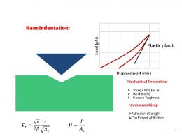
2 NANOINDENTATION ANALYSIS TECHNIQUE A typical load-penetration depth curve is shown in Figure 1, where hf is the final unloading depth, hmax the maximum loading depth during indentation tests, and Pmax the maximum load. S* is the slope of the tangent line to the unloading curve at the maximum loading point (hmax, Pmax) and is termed the
3
Proceedings of the IMechE, Part C: Journal of Mechanical Engineering Science, Vol. 221, 2007, pp. 259-266 system contact stiffness. hc is the intercept value of the above mentioned tangent line down to P=0 and is termed the contact depth. Unlike the conventional hardness experiment in which mechanical properties were calculated by directly measuring physical dimensions of the indention, the contact area should be calculated using empirical equations, and then mechanical properties are deduced in nanoindentation. P Pmax
unloading Loading
S*
hf
hc
hma
h
Figure 1. Schematic diagram of a nanoindentation load-penetration depth curve. Among the methods for analyzing load-penetration depth data [15-17], the one proposed by Oliver and Pharr is widely employed [18]. Their method assumes that the relationship between penetration depth h and load P for some given indenter geometry can be represented in the form
P = α (h − h f ) m where
α is
(1)
a fitting parameter which contains geometric constants, elastic modulus and Poisson‘s
ratio of the specimen and the indenter. m is a power law exponent related to the geometry of the indenter. For a flat-ended cylindrical punch, m=1; for a paraboloid of revolution, m=1.5; and for a cone m=2. The specimen contact stiffness is given by
S = 2aEr =
2β
π
Er A
(2)
where a is the contact radius and A the contact area. The reduced modulus Er, accounting for the deformation of both indenter and specimen, can be calculated by
4
Proceedings of the IMechE, Part C: Journal of Mechanical Engineering Science, Vol. 221, 2007, pp. 259-266
1 (1 − v 2 ) (1 − vi2 ) = + Er E Ei
(3)
where E and v are the elastic modulus and Poisson’s radio of specimen respectively, while Ei and vi are the elastic modulus and Poisson’s ratio of the indenter material respectively. The system stiffness S*, as defined above, is given below
⎛ dP ⎞ S* = ⎜ = αm( hmax − h f ) m−1 ⎟ ⎝ dh ⎠ (hmax , Pmax )
(4)
If h represents only the penetration depth of the indenter tip into the specimen, then S=S*. The contact depth hc is given by
hc = hmax −
εPmax S
(5)
whereεis associated with the specific tip geometry. Once the contact depth has been calculated, the contact area, A, can be obtained. For a perfect Berkovich indenter, A is given by
A( hc ) = 25.4hc2
(6)
The hardness H, in nano-scale regime, is defined as the mean pressure under the indenter:
H=
Pmax A
(7)
When the load-penetration depth data are obtained, the elastic modulus and hardness can then be calculated from Eqs. (1)~(7). Firstly, the unloading curves are fit to a power law function (see Eq. (1)), and the fitting parameters are used to calculate S* (see Eq. (4)), which is equal to S. S is then used to calculate hc (see Eq. (5)), and hc is used to calculate A from the shape area function of the tip. Finally, S and A are used to calculate E and H using Eqs. (2) and (7).
3 EXPERIMENT 3.1 Specimen Preparation The nanoindentation specimen was a single copper thin film fabricated by the vacuum vapor
5
Proceedings of the IMechE, Part C: Journal of Mechanical Engineering Science, Vol. 221, 2007, pp. 259-266 deposition technique on the surface of a silicon substrate. The film has an average thickness of 1.5μm. Since the specimen was kept at room temperature in the air, there was an oxide layer on the surface. In order to eliminate its influence, a rectangle area of 50μm×50μm without oxide was yielded prior to indentation by the scratch mode of AFM. The rectangle area has a surface roughness of 5 nm as measured by AFM.
3.2 Nanoindentation Procedure with the AFM Nanoindentation tests of the single copper thin film were carried out using an AFM (NanoscopeШa, Dimension3100, Digital Instruments, Santa Barbara, CA) with a diamond tip. The diamond tip mounted on a stainless steel cantilever is a Berkovich-like three-sided pyramid and its radius R measured by AFM in its contact mode with a silicon nitride tip is smaller than 20 nm. The spring constant kc of the steel cantilever is 230N/m as estimated by the supplier. Figure 2 illustrates a schematic diagram of the nanoindentation procedure with an AFM. The thickness and surface quality of the thin film were measured by the contact mode of AFM before the indentation tests (Step 1). Generally, when the indentaion depth does not exceed 10% of the specimen thickness, the substrate effect on the measurement could be neglected. Therefore, for the present specimen, the maximum indentation depth should not be deeper than 150nm. In addition, the minimum indentation depth should exceed the specimen surface roughness in order to obtain a discriminable indentation. As a preparatory step, the AFM instrumental uncertainties should be minimized (Step 2). Such a step includes using small ranges of Z motion, using the linear regime of photodiode, setting up high Z scan rates and an appropriate lateral compensation, etc. Then, the sensitivity of the cantilever was calibrated (Step 3), which is the ratio of the differential voltage obtained from the cantilever’s vertical deflection to the displacement of the piezoelectric actuator in the Z direction. The sensitivity of
6
Proceedings of the IMechE, Part C: Journal of Mechanical Engineering Science, Vol. 221, 2007, pp. 259-266 the cantilever calibrated on an “infinitely stiff” sapphire sample before and after indentation tests is 3.45V/μm. After the calibration, indentation tests were carried out using the indent mode of AFM provided by the AFM manufacturer (Step 4).
Step 1
Measurement of thickness
Step 2
Minimize the uncertainties
Step 3
Calibration of the sensitivity
Step 4 Nanoindentation tests
Step 5
Convert force curves to
Step 6
Calculation of elastic modulus
Figure 2. Schematic diagram of nanoindentation procedure with the AFM. In order to extract the mechanical properties from indentation tests, the force curves obtained by AFM should be converted to the load-penetration depth curves (Step 5). When a diamond tip penetrates the specimen surface, the displacement of the piezoelectric actuator in the Z direction results in both the cantilever’s deflection and the specimen indentation depth, the amounts of which depend on the relative stiffness of the specimen and the cantilever of AFM. The relationship between the displacement of the piezoelectric actuator ΔZ p , the cantilever’s deflection ΔZ c , and the specimen indentation depth ΔZ i , is given by
ΔZ p = ΔZ i + ΔZ c cos θ
(8)
where the θ corrects for the angle of the cantilever to the horizontal, and θ is 120 for this cantilever. The cantilever force, P, which equals to indentation load, can be calculated directly from ΔZ c , through
P = k c ΔZ c 7
(9)
Proceedings of the IMechE, Part C: Journal of Mechanical Engineering Science, Vol. 221, 2007, pp. 259-266 and
ΔZ c = Vdef / sensitivit y
(10)
where Vdef is the differential voltage, while the sensitivity has been calibrated as above. Finally, elastic modulus and hardness can be calculated by Oliver and Pharr method (Step 6).
4 MOLECULAR DYNAMICS SIMULATION 4.1 Interatomic potential The interatomic potential for Cu in this study is the embedded atom method (EAM) originally proposed by Daw and Baskes [19-20]. The EAM which was derived based on density functional theory has been widely applied in the simulation of many metallic systems because the simulation results have been reported in good agreement with experimental results. In order to reduce computational time and accelerate the force calculations of interacting atoms, a simplified form of the EAM proposed by Johnson [21] was adopted in this study. Johnson’s simple nearest neighbor analytical model takes into account the nearest neighbor contributions to the electron density and the two-body potential in the FCC lattice and is well suited to the MD simulation of metallic systems and FCC lattice metal in particular. Beside of EAM potential for interacting of Cu atoms, the Morse potential was adopted to describe the interaction between C and Cu atoms. In order to match the experiment above, the Cu-Cu, C-C and Cu-C Morse potentials have been determined. The parameters for Cu-C Morse potential have not been available and it is derived from standard Morse potential function based on a mix rule proposed by Rafii et al [22]. Based on the standard Morse potential, the interaction potential for Cu-Cu and C-C are:
ϕ Cu −Cu ( rij ) = DCu [exp( −2α Cu ( rij − rCu )) − 2 exp( −α Cu ( rij − rCu ))]
8
(11)
Proceedings of the IMechE, Part C: Journal of Mechanical Engineering Science, Vol. 221, 2007, pp. 259-266
ϕ C −C ( rij ) = DC [exp( −2α C (rij − rC )) − 2 exp( −α C (rij − rC ))]
(12)
A Morse-like potential energy function was assumed to describe the interactions between copper atoms and diamond atoms. The interaction potential for Cu- C is:
ϕ Cu −C (rij ) = DCu −C [exp( −2α Cu −C ( rij − rCu −C )) − 2 exp( −α Cu −C (rij − rCu −C ))] (13) The parameters for Cu-C Morse potential are obtained as follows
DCu −C = DCu DC
α Cu −C = α Cuα C rCu −C = rCu rC
(14)
The parameters for Cu-Cu Morse potential are obtained by fitting the experimental cohesive energy, lattice constant and bulk modules of single crystal copper and the parameters for C-C Morse potential are obtained by fitting the experimental cohesive energy, the inter-planar spacing and elastic constant of diamond crystal. The parameters for Cu and C Morse potentials are listed in Table 1 Table 1 Parameters for Cu and C Morse potential
α Cu
αC
DCu
1.359 Å
4.952 Å
0.34 ev
DC 3.1 ev
rCu 2.866 Å
rC 1.242 Å
The cutoff radius rc is chosen such that the ratio of the potential at the cutoff point to that at equilibrium is less than 4%. The use of such a cutoff radius ensures that the calculations will not consume large quantities of computational time in evaluating the forces that are near zero. The Morse potential parameters for Cu provided above were only for the calculation of the Morse potential parameters for interacting of Cu and C. In practice Johnson’s EAM potential was used for the interacting of Cu atoms.
9
Proceedings of the IMechE, Part C: Journal of Mechanical Engineering Science, Vol. 221, 2007, pp. 259-266
4.2 Nanoindentation Model Fig.3. shows a schematic diagram of the nanoindentation model used in MD simulation. The model consisted of the diamond indenter and the single crystal copper thin films specimen. The specimen is physically divided into three different regions, namely, Newtonian atoms region, thermostat atoms region and boundary atoms region. The thermostat atoms controlled the process temperature by adding or removing system energy. Boundary atoms are fixed on their perfect lattice sites to reduce the boundary effect, the periodic boundary conditions are not applied in this simulation.
Direction of indentation
Indenter
Newtonian atoms Thermostat atoms Boundary atoms
Single crystal copper specimen y
x z
Figure 3 A schematic MD model of nanoindentation. [100] direction is chosen as the indentation direction. The indentation speed of 20m/s is employed to reduce the computational time. Although this high speed compared to that of nanoindentation experiments with the AFM is unrealistic, it is proved that there is little influence on the understanding of the mechanism of nanoindentation process. The size of the specimen was 28a(x)×14a(y)×20a(z), where a is the lattice constant. The time step interval of MD simulation is taken to be 1×10-15s. The simulation is extended up to 120,000 steps. Initially, the atoms are positioned at the perfect lattice sites. The model is relaxed to equilibrium for a period of 50ps by controlling the internal temperature with a Nosé-Hover MD mothod [23] before the indenter load is applied. The temperature is controlled throughout the simulation. 10
Proceedings of the IMechE, Part C: Journal of Mechanical Engineering Science, Vol. 221, 2007, pp. 259-266 With the above Morse potentials available, the force on atom i owing to the interaction of other atoms can be calculated by N
Fi = −∑ ∇ϕ (rij )
(15)
j ≠i
where N is the total number of atoms in the model, including thermostat, boundary and diamond atoms. Consequently, the motion of all the Newtonian atoms in the control volume can be obtained by following Newton’s law
Fi = m
dri dt
(16)
The Verlet velocity algorithm is used to solve the Newton’s equation and a multi-processor workstation is used for running the simulation.
5 RESULTS AND DISCUSSION 5.1 Experimental Results Nanoindentation tests of the single crystal copper thin film were conducted for various differential voltages from 0.4V to 2.0V, stepped by 0.2V. Because each differential voltage corresponds to an indentation depth, the effect of indentation depth on mechanical properties can be investigated. Figure 4 shows an AFM image of single crystal copper thin film after the nanoindentation test.
2.0
1.8
1.6
1.4
1.2
1.0
0.8
0.6
0.4
Figure 4. An AFM image of the single crystal copper thin film after nanoindentation. The elastic modulus of the specimen under various indentation depths calculated from Eqs. (2) and (3) are listed in Table 2. The Poisson’s ratio is taken as 0.34. By now, the Poisson’s ratio and elastic
11
Proceedings of the IMechE, Part C: Journal of Mechanical Engineering Science, Vol. 221, 2007, pp. 259-266 modulus cannot be simultaneously deduced from naonindentation tests, and it is therefore necessary to assume a Poisson’s ratio for the thin film materials prior to calculation. The average elastic modulus is listed in Table 2. Table 2 Elastic modulus in single crystal copper thin film by nanoindentation Vdef(V) 0.4 0.6 0.8 1.0 1.2 1.4 1.6 1.8 2.0 Average
hf(nm) 16.32 20.70 29.54 36.94 45.42 53.53 54.36 60.65 66.74
hmax(nm) 25.95 34.93 46.70 62.25 70.15 77.83 81.81 95.79 103.76
hc(nm) 24.22 31.91 43.46 60.35 66.82 73.07 78.01 91.33 100.17
Pmax(μN) 27.02 40.54 54.05 67.57 81.08 94.60 108.11 121.63 135.14
Er(GPa) 78.6 80.4 71.7 78.0 67.8 60.2 64.6 70.0 68.0 71.0±6.8
E(GPa) 74.6 76.5 67.7 74.0 63.7 56.2 60.5 65.9 64.0 67.0±6.9
5.2 Simulation Results Fig 5(a)-(d) are MD simulation plots of nanoindentation of single crystal copper in (100) plane through the indenter tip, showing various stages of the nanoindentation process. Fig.5(a) shows the initial set-up of the specimen before commencing the indentation process, Fig 5(b) an intermediate stage during the indentation process, Fig. 5(c) the indenter at maximum indentation depth, and Fig. 5(d) the specimen after the indenter was retracted from it. Atoms around the indenter were pushed up and severely displaced as the indenter was penetrated into the surface of the specimen. The volume of specimen material displaced by the indentation was pushed out to the sides of the indenter and a pile-up of material was formed (Fig.5 (b-d)). This phenomenon was also observed in the nanoindentation experiment with the AFM (Fig. 4). The plastic deformation was limited to a few lattice spacing surrounding the indenter, and the rest of the specimen maintained basically its crystal structure. The plastically deformed region around the indenter has been referred to as amorphous copper. No dislocation was observed even at maximum indentation depth
12
Proceedings of the IMechE, Part C: Journal of Mechanical Engineering Science, Vol. 221, 2007, pp. 259-266 (Fig.5(c)). As the indenter was retracted from the specimen surface elastic recovery of the indent area was observed (Fig.5 (d)).
(a)
(b)
(c)
(d)
Figure 5. MD simulation plots of nanoindentation.
5.3 Discussion Elastic modulus of specimens under various indentation depths is 67.0±6.9GPa by the Oliver-Pharr method (Table 2) and there is no indentation size effects. The elastic modulus of the single crystal copper was reported ranging from 60GPa to 192GPa, so the results obtained from indentation tests using the AFM is in reasonable agreement with the simulation.
13
Proceedings of the IMechE, Part C: Journal of Mechanical Engineering Science, Vol. 221, 2007, pp. 259-266
Figure 6. Effect of indentation depths on hardness. Figure 6 shows the curve of the experimental hardness versus the maximum indentation depth obtained by Oliver-Pharr method. The experimental indentation hardness shows a constant increase with decreasing indentation depth, indicating a strong size effects arise because of geometrical constraints on dislocation motion. The hardness values and its size effects measured from this nanoindentation testing are in better agreement with the results reported by other researchers [24]. Due to the inaccuracy in the contact area calculation from Eq. (6), the values of hardness are slightly lower than their results. Size effects on mechanical properties starts to play a dominant role when one or more of the structural dimensions approaches down to the scale of micrometer or less. At such a size scale, there is no significant effect on the elastic properties of the materials since they depend on the bonding nature between the constituent atoms. MD simulation results show that the ratio of elastic recovery to the thickness of deformation region maintains constant basically as the indentation increases, which prove that elastic properties of the materials intrinsically depend on the cohesive energy between atoms and are insensitive to the size and the microstructure of materials. By contrast, the onset of plastic deformation strongly depends on dislocation mobility under an induced stress. The ease of their movement can be influenced by any number of obstacles such as grain boundaries, defects, surfaces, 14
Proceedings of the IMechE, Part C: Journal of Mechanical Engineering Science, Vol. 221, 2007, pp. 259-266 etc. Specimen size effects then begin to govern the plastic behavior by creating geometrical constraints, which obstruct dislocations to initiate and slide. MD simulations results also show that no distinct dislocations were observed and plastic deformation of nanoindentation on single crystal copper thin films via amorphous transformation is more favorable than via the generation and propagation of dislocations, unlike in bulk material, where the plastic deformation of crystalline solid is difficult without dislocations.
6 CONCLUSIONS In this study, the AFM system and molecular dynamics simulations have been successfully used to conduct nanoindentation tests of single crystal copper thin films. The following conclusions can be drawn from the investigation: (1) The elastic modulus of the film obtained from nanoindentation tests with the AFM is 67.0±6.9GPa which is in reasonable agreement with the results reported by other researchers. (2) Both AFM experiments and MD simulations results show that there is no size effect on elastic properties of materials, because elastic properties of the materials intrinsically depend on the cohesive energy between atoms and are insensitive to the size and the microstructure of materials. (3) A constant increase in the experimental indentation hardness was observed with decreasing indentation depth, indicating a strong size effect, which arises because of geometrical constraints on dislocation motion. MD Simulations results also show that due to size effect the plastic deformation via amorphous transformation is more favorable than via the generation and propagation of dislocations in nanoindentation of single crystal copper thin films. (4) The MD simulations are conducted on a relatively small-scale compared to the experiment, but the simulation results can illustrate many phenomena observed experimentally and provide an
15
Proceedings of the IMechE, Part C: Journal of Mechanical Engineering Science, Vol. 221, 2007, pp. 259-266 atomistic description. (5) The main limitations of the experimental method proposed in this study include the inaccuracy in the contact area calculation and the instrumental uncertainties of commercial AFM systems.
ACKNOWLEDGEMENTS The authors are grateful for the support of the EU 6th Framework NMP Program under the contract number NMP2-CT-2-4-500095 and the National Natural Science Foundation of China under the contract number 50175017.
REFERENCES [1]
Seo, C. T., Lee, J. H., Lee J. R. and Bae, Y. H. Fabrication of variable capacitor by thin copper film with electroplating. International Journal of Modern Physics B, 2003, 17(8-9), 2001-2004.
[2]
Zhang, G. P., Liu, Y. and Zhang, B. Deformation behavior of free-standing Pd-based thin film metallic glass for micro electro mechanical systems applications. Advanced Engineering Materials, 2005, 7(7), 606-609.
[3]
Inberg, A., Shacham-Diamand, Y., Rabinovich, E., Golanb, G. and Croitoru, N. Electroless-deposited Ag-W films for microelectronics applications. Thin Solid Films, 2001, 389 213-218.
[4]
Cao, D. M., Wang, T., Feng, B., Meng, W. J. and Kelly, K. W. Amorphous hydrocarbon based thin films for high-aspect-ratio MEMS applications. Thin Solid Films, 2001, 398-399, 553-559.
[5]
Abdelmalek, F. Study of the optical properties of corroded gold-aluminum films using surface plasmon resonances. Thin Solid Films, 2001, 389, 296-300.
[6]
Consiglio, R., Randall, N. X., and Bellaton, B. Nano-scratch tester (NST) as a new tool for assessing the strength of ultrathin hard coatings and the mar resistance of polymer. Thin Solid
16
Proceedings of the IMechE, Part C: Journal of Mechanical Engineering Science, Vol. 221, 2007, pp. 259-266 Films,1998, 332, 151-156. [7]
Li, J. C. M. Impression creep and other localized tests. Materials Science and Engineering A, 2002, 322, 23-42.
[8]
Chudoba, T. and Richter, F. Investigation of creep behaviour under load during indentation experiments and its influence on hardness and modulus results. Surface and Coatings Technology, 2001, 148, 191-198.
[9]
Li, X. and Bhushan, B. Micro/nanomechanical characterization of ceramic films for microdevices. Thin Solid Films, 1999, 340, 210-217.
[10] Chowdhury, S. and Laugier, M. T. Non-contact AFM with a nanoindentation technique for measuring the mechanical properties of thin films. Nanotechnology, 2004, 15(8), 1017-1022. [11] Nagy, P. M., Horvath, P., Kalman, E. and Kormos, F. Mechanical relaxation of SnO2 protective layers evaluated by nanoindentation and AFM. Materials and Manufacturing Processes, 2005, 20(1), 115-22. [12] Clifford, C. A. and Seah, M. P. Quantification issues in the identification of nanoscale regions of homopolymers using modulus measurement via AFM nanoindentation. Applied Surface Science, 2005, 252(5), 1915-1933. [13] Digital Instruments Inc. Support Note No.225, Rev F, 1998, Santa Barbara, CA [14] Knapp, J. A., Follstaedt, D. M., Myers, S. M., Barbour, J. C., Friedmann, T. A., Ager, J. W. III., Monteiro, O. R. and Brown, I. G. Finite-element modeling nanoindentation for evaluating mechanical properties of MEMS materials Surface and Coatings Technology, 1998, 103-104, 268-275. [15] Pethica, J. B., Huntchings, R. and Oliver, W. C. Hardness measurements at penetration depths
17
Proceedings of the IMechE, Part C: Journal of Mechanical Engineering Science, Vol. 221, 2007, pp. 259-266 as small as 20 nm. Philosophical Magazine A,1983, 48, 593-606. [16] Doerner, M. F. and Nix, W. D. A method for interpreting the data from depth-sensing indentation instruments. Journal of Materials Research,1986, 1, 601-609. [17] Briscoe, B. J., Sebastian, K. S. and Sinha, S. K. Application of the compliance method to microhardness measurements of organic polymers. Philosophical Magazine A, 1996, 74, 1159-1169. [18] Oliver, W. C. and Pharr, G. M. An improved technique for determining hardness and elastic modulus using load and displacement sensing indentation experiments. Journal of Materials Research, 1992, 7, 1564-1580. [19] Daw, M, S. and Baskes, M. I. Semiempirical, quantum mechanical calculation of hydrogen embrittlement in metals. Physical Review Letter, 1983, 50(17), 1285–1288. [20] Daw, M, S. and Baskes, M. I. Embedded-atom method: Derivation and application to impurities, surfaces, and other defects in metals. Physical Review B, 1984, 29, 6443–6453. [21] Johnson, R. A. Analytic nearest-neighbor model for fcc metals. Physical Review B, 1988, 37(8), 3924–3931. [22] Rafii-Tabar, H. Modelling the Nano-scale Phenomena in Condensed Matter Physics via Computer-based Numerical Simulations. Physics Reports, 2000, 325, 239-310. [23] Nosé, S. Constant temperature molecular dynamics methods. Progress of Theoretical Physics Supplement,1991, 103, 1-46. [24] Nix, W. D. and Gao, H. Indentation size effects in crystalline materials: a law for strain gradient plasticity. Journal of the Mechanics and Physics of Solids, 1998, 46, 411-425.
18