arXiv:quant-ph/9909070v1 22 Sep 1999. An optically driven quantum dot quantum computer ..... B 59, 2070 (1999). [13] D. G. Cory, M. D. Price, and T. F. Havel, ...
An optically driven quantum dot quantum computer G. D. Sanders, K. W. Kim, and W. C. Holton
arXiv:quant-ph/9909070v1 22 Sep 1999
Department of Electrical and Computer Engineering, North Carolina State University Raleigh, North Carolina 27695-7911
Abstract
We propose a quantum computer structure based on coupled asymmetric single-electron quantum dots. Adjacent dots are strongly coupled by means of electric dipole-dipole interactions enabling rapid computation rates. Further, the asymmetric structures can be tailored for a long coherence time. The result maximizes the number of computation cycles prior to loss of coherence. PACS Number(s): 03.67.Lx, 73.20.Dx, 85.30.Vw
Typeset using REVTEX 1
The possibility that a computer could be built employing the laws of quantum physics has stimulated considerable interest in searching for useful algorithms and a realizable physical implementation. Two useful algorithms, exhaustive search [1] and factorization [2], have been discovered; others have been shown possible. Various approaches have been explored for possible physical implementations, including trapped ions [3], cavity quantum electrodynamics [4], ensemble nuclear magnetic resonance [5], small Josephson junctions [6], optical devices incorporating beam splitters and phase shifters [7], and a number of solid state systems based on quantum dots [8–12]. There are many advantages to quantum computing; however, the requirements for such computers are very stringent, perhaps especially so for solid state systems. Nevertheless, solid state quantum computers are very appealing relative to other proposed physical implementations. For example, semiconductor-manufacturing technology is immediately applicable to the production of quantum computers of the proper implementation that is readily scalable due to its artificially fabricated nature. In this paper, we propose a manufactured solid state implementation based on advanced nanotechnology that seems capable of physical implementation. It consists of an ensemble of ”identical” semiconductor pillars, each consisting of a vertical stack of coupled asymmetric GaAs/AlGaAs single-electron quantum dots of differing sizes and material compositions so that each dot possesses a distinct energy structure. Qubit registers are based on the ground and first excited states of a single electron within each quantum dot. The asymmetric dots produce large built-in electrostatic dipole moments between the ground and excited states, and electrons in adjacent dots are coupled through an electric dipole-dipole interaction. The dipole-dipole coupling between electrons in nonadjacent dots is less by ten times the coupling between adjacent dots. Parameters of the structure can be chosen to produce a well-resolved spectrum of distinguishable qubits with adjacent qubits strongly coupled. The resulting ensemble of quantum computers may also be tuned electrically through metal interconnect to produce ”identical” pillars. In addition, the asymmetric potential can be designed so that dephasing due to electron-phonon scattering and spontaneous emission is minimized. The combination of strong dipole-dipole coupling and long dephasing times make it possible to perform many computational steps. Quantum computations may be carried out in complete analogy with the operation of a NMR quantum computer, including the application of refocusing pulses to decouple qubits not involved with a current step in the computational process [13]. Final readout of the amplitude and phase of the qubit states can be achieved through quantum state holography. Amplitude and phase information are extracted through mixing the final state with a reference state generated in the same system by an additional delayed laser pulse and detecting the total time- and frequency- integrated fluorescence as a function of the delay [14,15]. Means of characterizing the required laser pulses are described in Ref. [16]. Our quantum register is similar to the n-type single-electron transistor structure recently reported by Tarucha et al. [17]. In Tarucha’s structure, source and drain are at the top and bottom of a free standing pillar with a quantum well in the middle and a cylindrical gate wrapped around the center of the pillar. In our design, a stacked series of asymmetric GaAs/AlGaAs quantum wells are arrayed along the pillar axis by first epitaxially growing planar quantum wells in a manner similar to that employed to produce surface emitting lasers [18]. By applying a negative gate bias that depletes carriers near the surface, a parabolic electrostatic potential is formed which provides confinement in the radial direction. In the 2
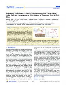
strong depletion regime, the curvature of the parabolic radial potential is a function of the doping concentration. To facilitate coupling to the laser field, the gate is made transparent using a reverse damascene process. The simultaneous insertion of a single electron in each dot is accomplished by lining up the quantum dot ground state levels so they lie close to the Fermi level; a single electron is confined in each dot over a finite range of the gate voltage due to shell filling effects [17]. Strong electrostatic confinement in the radial direction serves to keep the quantum dot electrons from interacting with the gate electrode, phonon surface modes, localized surface impurities, and interface roughness fluctuations. The electrostatic potential near the pillar axis is smooth in the presence of small fluctuations in the pillar radius. By tuning the gate voltage, it is anticipated that size fluctuations between different pillars can be compensated for. In order to derive the structure parameters and estimate the dependence of the functional performance of this device, we assume that the quantum dot electron potential, V(r), can be expressed in cylindrical coordinates as V (~r) = V (z) + V (ρ), where V (ρ) is a radial potential and V (z) is the potential along the growth direction. This separable potential assumption is a good approximation in the strong depletion regime where only a single electron resides in each dot. The assumption of a separable potential is commonly used in the study of quantum dot structures and enables us to consider the z and ρ motions separately [17,19]. The zdirectional potential V (z), shown schematically in the inset of Fig. 1, is a step potential formed by a layer of Alx Ga1−x As of thickness B (0 < z < B) and a layer of GaAs of thickness L − B (B < z < L). The resulting asymmetric quantum dot/well is confined by Aly Ga1−y As barriers with y > x. The asymmetry of this structure is parameterized by the ratio B/L where 0 < B/L < 1. In the effective mass approximation, the qubit wavefunctions are |ii = R(ρ) ψi (z) us (~r) (i = 0, 1). Here R(ρ) is the ground state of the radial envelope function, ψi (z) is the envelope function along z, and us (~r) is the s-like zone center Bloch function including electron spin. For simplicity, we assume complete confinement by the Aly Ga1−y As barriers along the z direction. Then, the envelope function ψi (z) is obtained by solving the time-independent Schr¨odinger equation subject to the boundary conditions ψi (0) = ψi (L) = 0. The energies of the qubit wavefunctions are given by E = Eρ + Ei where Eρ is the energy associated with R(ρ) and Ei is the energy associated with ψi (z). Since the present study primarily concerns coupling along the growth direction, analyses are conducted only in this direction. Figure 1 shows the probability density, |ψi (z)|2 , as a function of position, z, for the two qubit states |0i and |1i in a 20 nm GaAs/Al0.3 Ga0.7 As asymmetric quantum dot. The barrier thickness B = 15 nm and the overall length of the dot is L = 20 nm. By choosing B/L = 0.75 and x = 0.3, it is found that the ground state wavefunction |0i is strongly localized in the GaAs region while the |1i wavefunction is strongly localized in the Al0.3 Ga0.7 As barrier. By appropriately choosing the asymmetric quantum dot parameters, the qubit wavefunctions can be spatially separated and a large difference in the electrostatic dipole moments can be achieved. The transition energy ∆E = E1 −E0 between |1i and |0i is shown in Fig. 2 as a function of B/L in a 20 nm GaAs/Alx Ga1−x As asymmetric quantum dot (L = 20 nm). Several values of Al concentration x are considered. It is clear from this figure that the transition energy can be tailored substantially by varying the asymmetry parameter. With three parameters available for adjustment (B, L, and x), we can make ∆E unique for each dot in the register. 3
In this way, we can address a given dot by using laser light with the correct photon energy. The electric field from an electron in one dot shifts the energy levels of electrons in adjacent dots through electrostatic dipole-dipole coupling. By appropriate choice of coordinate systems, the dipole moments associated with |0i and |1i can be written equal in magnitude but oppositely directed. The dipole-dipole coupling energy is then defined as [8] Vdd = 2
|d1 | |d2 | , 3 ǫr R12
(1)
where d1 and d2 are the ground state dipole moments in the two dots, ǫr = 12.9 is the dielectric constant for GaAs, and R12 is the distance between the dots. Figure 3 shows the dipole-dipole coupling energy, Vdd , between two asymmetric GaAs/Alx Ga1−x As quantum dots of widths L1 = 19 nm and L2 = 21 nm separated by a 10 nm Aly Ga1−y As barrier. The coupling energy is plotted as a function of B/L for several values of x where B/L and x are taken to be the same in both dots. The dipole-dipole coupling energies are a strongly peaked function of the asymmetry parameter, B/L. From the figure, we see that values of Vdd ∼ 0.15 meV can be achieved. By way of comparison, the maximum dipole-dipole coupling energy that can be achieved with DC biased symmetric quantum dots (B/L = 0) is Vdd = 0.038 meV at a DC bias field of F = 112 kV /cm. Quantum dot electrons can interact with the environment through the phonon field, particularly the longitudinal-optical (LO) and acoustic (LA) phonons. The LO phonon energy, h ¯ ωLO , lies in a narrow band around 36.2 meV . As long as the quantum dot energy level spacings lie outside this band, LO phonon scattering is strongly suppressed by the phonon bottleneck effect. Acoustic phonon energies are much smaller than the energy difference, ∆E, between qubit states. Thus acoustic phonon scattering requires multiple emission processes which are also very slow. Theoretical studies on phonon bottleneck effects in GaAs quantum dots indicate that LO and LA phonon scattering rates including multiple phonon processes are slower than the spontaneous emission rate provided that the quantum dot energy level spacing is greater than ∼ 1 meV and, at the same time, avoids a narrow window (of a few meV) around the LO phonon energy [20]. While dephasing via interactions with the phonon field can be strongly suppressed by proper designing of the structure, quantum dot electrons are still coupled to the environment through spontaneous emission and this is the dominant dephasing mechanism. Decoherence resulting from spontaneous emission ultimately limits the total time available for a quantum computation [21]. Thus, it’s important that the spontaneous emission lifetime be large. The excited state lifetime, Td , against spontaneous emission is [21] Td =
3¯ h (¯ hc)3 , 4e2 D 2 ∆E 3
(2)
where D = h0|z|1i is the dipole matrix element between |0i and |1i. Figure 4 shows the spontaneous emission lifetime of an electron in qubit state |1i for a 20 nm GaAs/Alx Ga1−x As quantum dot as a function of asymmetry parameter, B/L, for several values of Aluminum concentration, x. It’s immediately obvious from Fig. 4 that the lifetime depends strongly on B/L. Depending on the value of x chosen, the computed lifetime can achieve a maximum of between 4000 ns and 6000 ns. In general, the maximum lifetime increases with x. In Eq. (2), the lifetime is inversely proportional to ∆E 3 and D 2 , 4
but the sharp peak seen in Fig. 4 is due primarily to a pronounced minimum in D. In contrast, the spontaneous emission lifetime in a 20 nm symmetric quantum dot under a DC bias of F = 112 kV /cm is only 1073 ns. Based on these results, we can estimate parameters for a solid state quantum register containing a stack of several asymmetric GaAs/Al0.3 Ga0.7 As quantum dots in the L ∼ 20 nm range separated by 10 nm Aly Ga1−y As barriers (y > 0.4). An important design goal is obtaining a large spontaneous emission lifetime and a large dipole-dipole coupling energy. From Figs. 3 and 4, we see that both can be achieved by selecting an asymmetry parameter, B/L = 0.8. This gives us a spontaneous emission lifetime Td = 3100 ns and a dipole-dipole coupling energy Vdd = 0.14 meV . The transition energy between the qubit states is on the order of 100 meV (λ = 12.4 µm). In a quantum computation, the quantum register is optically driven by a laser as described in Ref. [8]. In our example, we require a tunable IR laser in the 12 µm range so we can individually address various transitions between coupled qubit states. Following initial state preparation, which can be achieved by cooling the structure to low temperature, the computation is driven by applying a series of coherent optical pulses at appropriate intervals. The π-pulse duration, Tp , must be less than the dephasing time, Td so that many computation steps can be performed before decoherence sets in. At the same time, the pulse linewidth must be narrow enough so that we can selectively excite transitions separated by the dipole-dipole coupling energy, Vdd . For transform limited ultrashort pulses, the linewidth-pulsewidth product is given by the Heisenberg uncertainty principle. Combining these two restraints, Tp must satisfy h ¯ ≪ Tp ≪ Td . 2 Vdd
(3)
Using Vdd and Td for our structure, we obtain 2.4 ps ≪ Tp ≪ 3.1 × 10⁶ ps. For highly biased symmetric quantum dots, it is 8.7 ps ≪ Tp ≪ 1.1 × 10⁶ ps using values of Vdd = 0.038 meV and Td = 1073 ns. Hence, the number of computational steps that can be executed before decoherence sets in (i.e., ratio of the upper and lower limits in the inequality) is an order of magnitude larger for the proposed asymmetric structure. In summary, we have proposed a solid state quantum register based on a vertically coupled asymmetric single-electron quantum dot structure that overcomes the problems of weak dipole-dipole coupling and short decoherence times encountered in earlier quantum dot computing schemes based on biased symmetric dots. This structure may provide a realistic candidate for quantum computing in solid state systems. This work was supported, in part, by the Defense Advanced Research Project Agency and the Office of Naval Research.
5
REFERENCES [1] L. K. Grover, Phys. Rev. Lett. 79, 325 (1997). [2] P. W. Shor, ”Algorithms for quantum computation: Discrete logarithms and factoring,” in Proceedings of the 35th Annual IEEE Symposium on Foundations of Computer Science (IEEE Computer Society Press, Los Alamitos, CA, 1994), pp. 124-134. [3] J. I. Cirac and P. Zoller, Phys. Rev. Lett. 74, 4091 (1995); C. Monroe, D. M. Meekhof, B. E. King, W. M. Itano, and D. J. Wineland, Phys. Rev. Lett. 75, 4714 (1995). [4] T. Pellizzari, S. A. Gardiner, J. I. Cirac, and P. Zoller, Phys. Rev. Lett. 75, 3788 (1995); Q. A. Turchette, C. J. Hood, W. Lange, H. Mabuchi, and H. J. Kimble, Phys. Rev. Lett. 75, 4710 (1995). [5] I. L. Chuang, N. Gershenfeld, and M. Kubinec, Phys. Rev. Lett. 80, 3408 (1998); D. G. Cory, M. D. Price, W. Maas, E. Knill, R. Laflamme, W. H. Zurek, T. F. Harvel, and S. S. Somaroo, Phys. Rev. Lett. 81, 2152 (1998). [6] A. Shnirman, G. Sch¨on, and Z. Hermon, Phys. Rev. Lett. 79, 2371 (1977). [7] N. J. Cerf, C. Adami, and P. G. Kwiat, Phys. Rev. A 57, R1477 (1998). [8] A. Barenco, D. Deustch, A. Ekert, and R. Jozsa, Phys. Rev. Lett. 74, 4083 (1995). [9] A. A. Baladin and K. L. Wang, private communication. [10] B. E. Kane, Nature 393, 133 (1998). [11] T. Tanamoto, Los Alamos preprint quant-ph 9902031 (1999). [12] D. Loss and D. P. DiVincenzo, Phys. Rev. A 57, 120 (1998); G. Burkard, D. Loss, and D. P. DiVincenzo, Phys. Rev. B 59, 2070 (1999). [13] D. G. Cory, M. D. Price, and T. F. Havel, Physica D, 120, 82 (1998); G. C. Cory, A. E. Dunlop, T. F. Havel, S. S. Somaroo, and W. Zhang, quant-ph 9809045 (1998). [14] C. Leichtle, W. P. Schleich, I. Sh. Averbukh, and M. Shapiro, Phys. Rev. Lett. 80, 1418 (1995); [15] T. C. Weinacht, J. Ahn, and P. H. Bucksbaum, Phys. Rev. Lett. 80, 5508 (1998); T. C. Weinacht, J. Ahn, and P. H. Buchsbaum Nature, 397, 233 (1999). [16] R. Trebino, K. W. DeLong, D. N. Fittinghoff, J. N. Sweetser, M. A. Krumbugel, B. A. Richman, and D. J. Kane, Rev. Sci. Inst., 68, 3277 (1997). [17] S. Tarucha, D. G. Austing, T. Honda, R. J. van der Hage, and L. P. Kouwenhoven, Phys. Rev. Lett. 77, 3613 (1996). [18] X. Zhang, Y. Yuan, A. Gutierrez-Aitken, and P. Bhattacharya, Appl. Phys. Lett. 69, 2309 (1996); K. Fujiwara, Shin-ichi Hinooda, and K. Kawashima, Appl. Phys. Lett. 71, 113 (1997). [19] L. Jacak, P. Hawrylak, and A. W`ojs, Quantum Dots (Springer-Verlag, New York, 1998). [20] T. Inoshita and H. Sakaki, Phys. Rev. B 46, 7260 (1992); U. Bockelman and G. Bastard, Phys. Rev. B 42, 8947 (1990); H. Benisty, Phys. Rev. B 51, 13281 (1995). [21] A. Ekert and R. Jozsa, Rev. Mod. Phys. 68, 733 (1996).
6
FIGURES FIG. 1. Probability density along the confinement direction, z, for the qubit wavefunctions |0i (solid line) and |1i (dot-dashed line). The inset shows a schematic illustration of the conduction bandedge profile in the z direction. FIG. 2. Transition energy, ∆E, between |0i and |1i in an L = 20 nm GaAs/Alx Ga1−x As asymmetric quantum dot as a function of B/L for several values of x. FIG. 3. Dipole-dipole interaction between two asymmetric GaAs/Alx Ga1−x As quantum dots of widths L1 = 19 nm and L2 = 21 nm separated by an Aly Ga1−y As barrier of width W b = 10 nm. The coupling energy is plotted as a function of B/L for several values of x. B/L and x are the same for both dots. FIG. 4. Spontaneous emission lifetime for qubit state |1i in a GaAs/Alx Ga1−x As quantum dot with L = 20 nm as a function of B/L for several values of x.
7
Sanders et al, Fig 1
Probability Density (1/nm)
0.3 L
L = 20 nm B = 15 nm
0.2
|0> x = 0.3
B
0.1
|1> B
0.0
0
5
10 Position (nm)
15
20
Sanders et al, Fig. 2
300
Energy Gap (meV)
L = 20 nm
200
x = 0.4 x = 0.3 x = 0.2 x = 0.1
100
0 0.0
0.2
0.4
0.6 B/L
0.8
1.0
Sanders et al, Fig. 3
Dipole−dipole coupling (meV)
0.20 L1 = 19 nm 0.15
L2 = 21 nm Wb = 10 nm
0.10
x = 0.1 x = 0.2 x = 0.3 x = 0.4
0.05
0.00 0.0
0.2
0.4
0.6 B/L
0.8
1.0
Sanders et al, Fig. 4
Spontaneous Emission Lifetime (ns)
8000 L = 20 nm 6000
4000
x = 0.1 x = 0.2 x = 0.3 x = 0.4
2000
0 0.0
0.2
0.4
0.6 B/L
0.8
1.0