XXII Conference on Design of Circuits and Integrated Systems
ISBN-13 978-84690-8629-2
Application of FPGA Emulation to SoC Floorplan and Packaging Exploration Pablo G. Del Valle⋆ , David Atienza† ⋆, Giacomo Paci‡ , Francesco Poletti‡ , Luca Benini‡ , Giovanni De Micheli† , Jose M. Mendias⋆ , Roman Hermida⋆ ⋆ DACYA/UCM, Profesor Jose Garcia Santesmases s/n, 28040 Madrid, Spain. E-mails:
[email protected], {datienza, mendias, rhermida}@dacya.ucm.es † LSI/EPFL, EPFL-IC-ISIM-LSI Station 14, 1015 Lausanne, Switzerland. E-mails: {david.atienza, giovanni.demicheli}@epfl.ch ‡ DEIS/Bologna, Viale Risorgimento 2, 40136 Bologna, Italy. E-mails: {gpaci, fpoletti, lbenini}@deis.unibo.it Abstract— New tendencies in the consumer electronics market present Multi-Processor Systems-On-Chip (MPSoCs) as a promising solution for meeting the processing demands of upcoming generations of user applications. MPSoCs are complex to design, as they must execute multiple applications (real-time video processing, 3D games), while meeting additional design constraints (energy consumption, time-to-market). When an integrated system is built for a certain MPSoC, the definition of an appropriate floorplan is a very complex task for system integration designers. In fact, deciding a suitable placement of each block in the MPSoC architecture requires taking into account multiple constraints (e.g., power, energy, performance, etc) with values that are specific for each design. Recently, due to the increasing temperature in MPSoCs, thermal behavior has become another key factor to define the placement of each block of the design. In this context, we show how designers will benefit from applying our FPGA-based Emulation Framework to the MPSoC design cycle. Starting with a set of constrains (performance, latency...) and the HW elements of the system, with the help of our exploration tool, the thermal behaviour of different floorplan alternatives can be profiled at an early stage of the development cycle. It will also guide the designer in selecting the right packaging solution for the final chip, minimizing the cost without compromising the chip reliability. Our platform enables thermal monitorization of the final (real) applications over the different architectures, at speeds very close to real time, as opposed to SW simulators.
I. I NTRODUCTION The increasing complexity of recent SoC designs has definitely modified the clasic design cycle. Due to the time-to-market factor, it is not possible anymore to build these systems from scratch. Multi-Processor Systems-on-Chip (MPSoCs) have been proposed as a promising solution for this context, since they are single-chip architectures consisting of complex integrated components (IP-Cores) communicating with each other at very high speeds [16]. The concept of IP-Cores seems to have relieved designers from dealing with the low level implementation details, (every core is independent, and tipically it has been verified by third party manufacturers). In theory, designing is just a matter of putting together different blocks and interconnecting them, thus, rising the abstraction level. Nevertheless, in practice, some new challenges make even more necessary than ever the need to be aware of the physical aspects of the design. Lets take a look at the insides of today’s chips: Several on-chip clocks: With the scaling of the technology, It is not possible to cover the whole die with only one clock source. Related logic must be placed together sharing the same clock. Synchronization methods have to be implemented among different clock domains. Bandwidth/latency requirements: Bus contention problems create the need for complex interconnection schemes (Networks-on-Chip). The logic density of this kind of designs coupled with very demanding SW applications can lead to generation of hot spots that
236
compromise the chip reliability [23] With these schema, new design constrains need to be taken into account. Temperature is now a major concern. In the past, thermal problems were solved out by improving the packaging solution, but now, designing a chip for the worse-case scenario often makes the final product prohibitibely expensive, and sometimes not even possible to manufacture (due to space constrains in the embedded systems). Recent studies have demonstrated that an intelligent placement of cores can reduce the thermal gradient of the chip, therefore improving the system robustness and reliability. This is an interesting research line in future MPSoCs, called temperatureaware placement [25], [26], [30]. In this case, the temperature issues are addressed at design-time to ensure that circuit blocks are placed in such a way that they even out the thermal profile. Also, by adding techniques (SW- or HW- based) for limiting the maximum allowable temperature (dynamic thermal management), we can reduce the packaging cost as well. In both cases, designers need from exhaustive system profiling to discover the best tradeoff: performance vs peak temperature or cost. Of course, each design is different, so the goals are not always the same. Sometimes there is a need for performance at no matter what cost, while in another situation, the designer may be looking for the cheapest chip, the higest power-efficiency or the most reliable design. Therefore, one of their main design challenges is the fast exploration of multiple hardware (HW) and software (SW) implementation alternatives with accurate estimations of performance, energy, power and temperature to tune the MPSoC architecture in an early stage of the design process. In our previous work we have developed a cycle-accurate HW emulation platform [3], which can obtain detailed reports of the thermal features of MPSoCs. In this paper, we explore the design space of different floorplan and packaging alternatives for latest MPSoCs. We use as case studies two real-life MPSoC architectures and their associated applications. In the first set of experiments, we compare three different chip layouts. The chip funtionality is the same in these three cases, but from the thermal point of view, they show different behaviours. Hence, as the cost is alike, our exploration guides the designer to select the one with the best thermal properties. In the second set of experiments, both the chip functionality and the floorplan remain unaltered, but we vary the packaging technology of the final chip. In this case, we explore the benefits and drawbacks of employing different solutions within the range of low-cost SoCs to high-performance solutions. Our results show that different trade-offs exist for the designer between the different packaging options according to the desired performance and temperature-rise tolerance. Furthermore, the possible addition of onchip Dynamic Thermal Management (DTM) techniques in the final
SoC creates an additional degree of freedom to take into account when the packaging option is selected The remainder of the paper is organized as follows. In Section II, we overview related work on MPSoC modeling, testing and thermalaware design. In Section III, we present the FPGA-based emulation framework and explain how it works. In Section IV we detail the setup for the presented set of experiments. Next, in Section V we show in detail the experiments performed, together with the obtained results, illustrating the speed and versatility of our thermal emulation tool for MPSoC designers. Finally, we draw our conclusions and dedicate some lines to possible future work in Section VI. II. R ELATED W ORK The future of the embedded systems envisages MPSoCs as a promising solution for the consumer electronics market [16]. According to this, research efforts for improving the tasks of modeling and prototyping MPSoC designs are in great need. One of the biggest problems when exploring the MPSoC design space is that the evaluation of each of the implementation alternatives (e.g. selecting the appropriate placement of all the cores) takes a considerably amount of time. The most common exploration method is the use of SW simulators that only achive a few Khz’s when used for accurate profiling. A typical workaround to solve this issue is to use models with higher abstraction levels that, although being faster alternatives, have the disadvantage of the loss of accuracy, feature that makes them bad candidates for exploring thermal properties. Another way to tackle the problem is the use of HW prototyping environments, faster than SW simulators, but in this case, they are tipically very expensive, and not flexible enough. At some point in between these two options is HW emulation, i.e. Zebu-XL [9], [2], [21], System Explore [1]. In [3] it has been presented a HW-SW emulation framework that offers the necessary accuracy levels while running at Mhz speeds. In this paper we compare the performance of our emulation results with the MPARM SW simulator. The MPARM SystemC framework [4] is a complete simulator for system-exploration. It can extract reliable energy and performance figures. As most of these tools, its major shortcoming is its simulation speed (120 KHz in a P-IV at 2.8 GHz). Regarding thermal modeling, several thermal/power models are being developed for predicting on-chip temperatures [23]. The main conclusion is that in forthcoming generations of embedded systems, thermal issues will gain more importance. To be noted that they already limit/reduce performance and affect leakage power of current designs. Using these thermal modeling tools, researchers are starting to propose different design solutions to overcome on-chip temperature problems. Several Dynamic Thermal Management (DTM) techniques have been suggested for processors using both architectural adaptation (e.g., Dynamic Voltage Scaling (DVS), Dynamic Frequency Scaling (DFS), fetch-toggling, throttling, and speculation control) and profiling-based techniques (e.g. those based on feedback control theory). Since these countermeasures typically decrease system performance, they are usually triggered when the power consumption of a processor crosses a predetermined threshold (e.g. not to schedule hot tasks when the temperature reaches a critical level [31]), or its workload decreases. III. OVERVIEW OF THE MPS O C E MULATION F RAMEWORK As presented in [3], our emulation platform is composed of different parts. Physically, it is an FPGA connected to a host pc through an ethernet cable. A system that emulates the designed
237
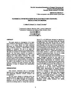
Fig. 1.
Overview of the emulation framework
target architecture is mapped inside the FPGA, together with the statistics extraction system, a completely transparent element that continuously monitors the emulation, logs the required information, and periodically sends it to the host pc. Inside the computer, this data is input to a SW thermal library that receives activity indicator values and outputs temperatures. These temperatures are then fed back into the FPGA and written to our artificial temperature sensors, that can be accessed from the emulated system, thus converting it into a thermal-aware platform. This very important feature allows the system to trigger dynamic frequency scaling mechanisms at run-time, based on the stimated on-chip temperature. In fact, a simple DFS mechanism based on previous works is presented in our experiments to illustrate the flexibility of the proposed HW-SW FPGA-based framework to interact with the SW part and to explore in real-time different temperature-management policies. By using our tool, designers are able to tune their applications to meet not only the performance constrains, but also the thermal limitations given by the selected packaging solution. On the HW part, the designer can experiment with diffent floorplan configurations (calculated automatically or by hand), as well as modify the packaging of the chip, (depending, of course, on the budget limitations). Regarding the SW thermal library, we consider MPSoCs HW that are made of silicon die wrapped into a package placed on a Printed Circuit Board (PCB), with a variable cost (from low-cost to high-cost packaging, shown in Section V). In this case, see Figure 2, the heat flow starts from the bottom surface of the die and goes up to the silicon, passes through the heat spreader and ends at the environment interface, where the heat is spread by natural convection [23]. For modeling the heat flow, we rely on an electrical RC model (see [3]) that splits the floorplan into small cells, each of them presents its resistance to the flowing current. This analogy mimics the way the heat transfers occur. Currently, we can analyze 2 seconds of simulation (in a 660-cell floorplan), in 1.65 seconds on a P-4 at 3GHz, which is fast enough to interact in real-time with our FPGA-based MPSoC emulation. On the other hand, we have cross-checked our results by including in our tool the possibility to use the Hotspot v3.0 thermal model [23]. In order to perform all the temperature calculations, the thermal library needs to know some architectural parameters at compile time (size and placement of all the components of the system (i.e., floorplan layout), technology and packaging information), as well as some others needed at run-time (current frequency of the different parts of the system, number of accesses to the resources,
Heat spreader IC die
IC package
1200um dCache iCache dCache iCache 8KB 8KB 8KB 8KB p1 p2 p1 p2
package pin
PCB Fig. 2.
Chip packaging solution
Processor1
Processor2
Private 32KB memory p3
NoC 6x6 switch p1
NoC 6x6 switch p2
NoC 6x6 switch p3
Private 32KB memory p1
Private 32KB memory p2
iCache dCache 8KB 8KB p3 p3
Private 32KB memory p4
NoC 6x6 switch p4
Fig. 3.
Overview HW architecture of emulated MPSoCs
bus congestion). IV. MPS O C R EAL -L IFE C ASE S TUDIES Our experiments include the application of the presented framework to test a run-time DFS mechanism for one complex MPSoC case study based on ARM-7 cores (Section V), and with different thermal-aware floorplan solutions (Section V-A) and various packaging techniques (Section V-B). 1) HW Architecture: As explained in Section V, we evaluate three different floorplans for a real-life MPSoC example. The first of them (Figure 4) has been manually designed, while the other two, (Figure 5(a)) and (Figure 5(b)), have been automatically generated by a placing tool. An schematical overview of the common baseline HW architecture of the emulated MPSoCs is depicted in Figure 3. It consists of three main elements: 1) 4 processing ARM7 cores running at 100 MHz or 500 MHz, 0.13 µm technology. 2) The definition of configurable I- and D-cache, as well as main memories (i.e., private and shared memories between processors). 3) Interconnection mechanisms (buses and NoCs) between the different levels of the memory hierarchy (caches and main memories). The interconnect is clocked at the same frequency that the cores in each case. The cell sizes (for the SW library) used in all cases are 150um ∗ 150um. We assume that the power is uniformly burned in this region, which represents 1/8th of the size of an ARM processor in 0.13 µm. For technologies with a worse thermal conductance, such as, fully depleted silicon-on-insulator [24], it is possible to use smaller thermal cells (down to the level of standard cells). Of course, all the necessary HW sniffers [3] as well as the emulation mechanism have been instantiated and connected to conform the overall system.
238
Shared 32KB memory
Processor4 iCache dCache 8KB 8KB p4 p4
Fig. 4.
Processor3
NoC interface
Original floorplan
2) SW Driver: As SW driver for this MPSoC design, we defined a benchmark (Matrix-TM) that keeps the workload of the processors close to 100% all the time, pushing the MPSoC to its processing power limits to observe effects in temperature. This benchmark implements a pipeline of 100K matrix multiplications kernels. Each processor executes a matrix multiplication between an input matrix and a private operand matrix, then feeds its output to the logically following processor. The platform receives a continuous flow of input matrices and produces a continuous flow of output matrices. Every core follows a fixed execution pattern: (i) copy of an input matrix from the shared memory to its private memory; (ii) multiplication of the new matrix with a matrix already stored in the private memory; (iii) copy of the resulting matrix back to the shared memory. During the whole execution, interrupt and/or semaphore slaves are queried to keep synchronization, creating an important amount of traffic to the memories. V. E XPERIMENTAL R ESULTS A. Floorplan selection exploration in MPSoCs When an integrated system is built for a certain MPSoC, the definition of an appropriate floorplan is a very complex task for system integration designers. In fact, deciding a suitable placement of each block in the MPSoC architecture requires taking into account multiple constraints (e.g., power, energy, performance, etc) with values that are specific for each design. Recently, due to the increasing temperature in MPSoCs, thermal behavior has become another key factor to define the placement of each block of the design [25], [26]. In this set of experiments, we have used our tool to evaluate three different chip layouts: one baseline floorplan (Figure 4), and two additional floorplans (Figure 5) (all of them are thermal-aware). The initial case study is composed of four processing cores and NoCbased interconnect working at 500 MHz (see Figure 4). The first alternative floorplan scatters the processing cores in the corners of the chip (Figure 5(a)), while in the second one all the cores are clustered together in the center of the chip (Figure 5(b)). We assumed the use of a low-cost packaging solution in all the cases (40K/W, see Section VI ). The results are shown in Figure 6. In this case we can observe that the best floorplan to minimize temperature (15% less heating speed on average than the initial floorplan of Figure 4) was achieved with the placement technique that tries to assign the processing cores to the corners of the layout (labelled as scattered in Figure 6). Hence, this solution is the best out of the three thermal-aware placement options because it delays the most the need to apply the available
1200um
1200um
dCache iCache 8KB 8KB p1 p1 Processor1 NoC 6x6 switch p1
Private 32KB memory p1 NoC 6x6 switch p3
Processor3 iCache dCache 8KB 8KB p3 p3
dCache iCache 8KB 8KB p2 p2 Private 32KB memory p2
Shared 32KB memory
Private 32KB memory p3
(a)
Processor2 NoC 6x6 switch p2
Private 32KB memory p4 NoC 6x6 switch p4
Processor4 iCache dCache 8KB 8KB p4 p4
Private 32KB memory p1
NoC 6x6 switch p1
Private 32KB memory p2
dCache iCache dCache iCache 8KB 8KB 8KB 8KB NoC 6x6 p1 p2 p1 p2 switch p2
Processor1 Processor2
NoC 6x6 Processor3 Processor4 dCache switch 8KB p3 iCache dCache iCache p4
8KB p3
Private 32KB memory p3
8KB p3
8KB p4
Shared 32KB memory
NoC 6x6 switch p4
Private 32KB memory p4
(b)
Fig. 5. MPSoC floorplan with cores (a) scattered in the corners and (b) clustered together in the center of the chip
DFS mechanism in Figure 6, although its interconnects experience more heating effects due to the longer and more conflicting connection paths between components, which can originate more NoC congestion effects. Then, the solution that tries to place all the processing cores in the center of the chip (labelled as clustered in Figure 6) shows the worst thermal behavior, but just slightly worst in temperature (5% on average) than the original manual placement of cores used for this MPSoC design, while the delays in the interconnections between cores are minimal for the former due to their closest locations in the floorplan (see Figure 5(b)). The main conclusion from this study is that a more aggresive temperature-aware placement must be applied (e.g., placement of cores scattered in the corners of the chip) to justify the placement of cores apart, as tried in the original manual design, to compensate for the heating effects on the chip due to longer interconnects. Otherwise, the possible penalty for long interconnects may not be justified in the end since a uniform distribution of power sources does not need to lead to a uniform temperature on the die. Moreover, these results clearly outline the importance for designers of tools to explore the specific thermal behavior of each design, and to select the most appropriate placement in an early stage of the integration flow. Note that in the figure it has also been included a series of data labeled as ”MPARM”. We have assessed the performance and flexibility of the proposed emulation framework in comparison with the MPARM framework [4] and its internal SW thermal library. As explained, this is a clasical (only SW) architecture simulator that lacks from the speed up of emulation. The small circle around the origin represents the simulated time for MPARM when the emulation finished (In our experiments MPARM is executed on a P-IV at 3.0 GHz with 1 GByte SDRAM and running GNU/Linux 2.6). B. Effect of different packaging technologies and SW thermal libraries In this final set of experiments we have tested different packaging solutions and compared them with the thermal behavior of the lowcost value of 40K/W initially considered for our initial reference of MPSoC floorplan with four RISC-32 processing cores working at 500 MHz and NoC interconnect (Figure 4). We simulated this floorplan with two additional values, namely, 12K/W in the case of standard packaging [27] and 5K/W in the case of high-cost and high-performance embedded processors [28]. The results obtained are shown in Figure 7. As this figure shows, in the case of the standard packaging solution, the MPSoC design required more time to heat up and it reached a maximum value of 360 degrees Kelvin when the DFS mechanism
239
Fig. 6. Average temperature evolution with different floorplans for MatrixTM at 500 MHz with DFS on
Fig. 7. Thermal behavior for an MPSoC floorplan using low-cost, standard and high-cost packaging solutions
was not applied, which is lower than the case of low-cost packaging (40K/W) that reached a temperature of more than 500 degrees Kelvin. However, the thermal behavior of the standard packaging system was similar to the low-cost solution (only its starting point was slightly shifted to the right due to the less steep temperature rise curve) when the threshold-based DTM strategy was applied (As observed in the figures, the temperature threshold was fixed at 250 degrees Kelvin. Each time a part of the system reaches this temperature, an automatic response is triggered, that reduces the running frequency from 500 MHz to 100 MHz). Therefore, in this case, with this threshold value, no significant improvements were obtained with the standard package, and the low-cost solution would be preferably selected for this design using DTM. However, in the case of the highcost packaging solution (for 5K/W), the system showed a completely different temperature behavior, where the chip never went beyond 325 degrees Kelvin. Therefore, this packaging solution creates a much lower thermal stress in the overall MPSoC implementation, and it does not require the application of DFS because the design never reaches a temperature above the 350-degree-Kelvin threshold. As a result, this solution could significantly increase the expected mean-time-to-failure of the component and be interesting in highly reliable versions of this MPSoC chip design. However, note that this type of package has the important drawback of the high cost for the manufacturer of the final embedded system, namely, typically 5 to 12× more than standard package solutions and more than 20× the low-cost package solution [29]; Thus, it can seriously increase the price of the final product and developers would like to avoid it if possible. Hence, this type of experiments and the presented
framework can be a very powerful tool for designers to decide which type of packaging technique would be enough for a specific set of constraints in forthcoming generations of MPSoC designs. Finally, we performed the same set of emulation experiments replacing our library with the well-known Hotspot v3.0 thermal library [23], configuring it with the same packaging options previously tested. The results of this additional set of experiments shown a very similar thermal behavior with this second RC thermal library in comparison to our own library in the case of high-cost packaging (less than 3 degrees Kelvin of difference), which is the original target of the Hotspot library. Then, in the case of low-cost and standard packaging, variations that range between 4-15 degrees Kelvin have been observed. The origin of these variations come from the non-linear dependency factor of silicon thermal conductivity with respect to the actual temperature in the die, which is included in our own library, but is not modeled in the Hotspot library. In fact, our results indicate that this non-linear part of the thermal equations is particularly important when the temperature rises beyond 360 degrees Kelvin in the case of low-cost packaging solutions, and needs to be considered at each moment of the emulation to get accurate thermal measurements for this type of MPSoC packaging technology.
but will gain importance in future SoCs generations. Since we are emulating, no modification would be necessary into the VHDL code describing the HW system. Only the SW thermal library needs to be modified to support the modeling of this kind of layouts. VII. ACKNOWLEDGMENTS This work is partially supported by the Spanish Government Research Grants TIN2005-5619 and FPU AP2005-0073, the Swiss NSF Research Grant 20021-109450/1 and the SRC Contract 1188. R EFERENCES [1] [2] [3] [4] [5] [6] [7] [8]
VI. C ONCLUSIONS AND F UTURE W ORK
[9]
Future consumer devices based on MPSoC architectures will contain a really large amount of transistors thanks to nanoscale technologies, but will be very complex to design as they must execute multiple complex real-time applications (e.g., video processing or 3D games), while meeting several additional design constraints (e.g., energy consumption or short time-to-market). Moreover, the rise of temperature in the die for on-chip components can seriously affect performance and reliability of final MPSoC designs. In this paper we have used our tool to evaluate different temperature-aware placement techniques that try to compensate the heating effects on MPSoCs. Our study indicates that significant overheads of power dissipated in long interconnects can clearly affect the overall thermal behavior of the final MPSoC, and that a uniform distribution of power sources in the die does not need to produce a uniform temperature in the final chip. Hence, MPSoCs designed in latest technology nodes require the use of tools to study their suitable placement in an early stage of system integration, according to the applications that will be executed in each final MPSoC. Also, we have illustrated the effectiveness of the presented thermal evaluation tool to rapidly study the effects of different packaging options for concrete MPSoC solutions. Our results indicate that the selection of final packaging solutions clearly depend on the thermal management techniques included in the target MPSoCs and more costly packagings may show from the same heating effects as lowcost ones; Thus, the need of expensive packaging solutions cannot be justified without prior extensive thermal exploration. Finally, we have shown the versatility of our tool to use various thermal libraries, and illustrated the need for different thermal models according to the implementation requirements of the target MPSoCs (e.g., high- or low-cost packaging). Having demonstrated the versatility and benefits of our emulation framework for MPSoC design exploration, one possible future line of research is to study the application and testing of complex dynamic thermal management policies to the emulated MPSoC. In this context, we are currently developing a library that offers complete support for testing advanced task migration policies. On the architectural part, it is possible to extend the emulation platform to be able to model the state-of-the-art 3D floorplans[30]. They are a very recent proposal,
[10]
240
[11] [12] [13] [14] [15] [16] [17] [18] [19] [20] [21] [22] [23] [24] [25] [26] [27] [28] [29] [30] [31]
Aptix System explore, 2003. http://www.aptix.com. ARM integrator AP, 2004. http://www.arm.com. Reference ommited for blind review L. Benini, et al. Mparm: Exploring the MPSoC design space with SystemC. Journal of VLSI, September 2005. N. Genko, et al. A Complete Network-On-Chip Emulation Framework. In Proc. of DATE, 2005. G. Braun, et al. Processor/memory co-exploration on multiple abstraction levels. In Proc. of DATE, 2003. CoWare. Convergensc and LisaTek product lines, 2004. http://www. coware.com. M. Diaz Nava, et al. An open platform for developing MPSoCs. IEEE Computer, pp. 60–67, July 2005. Emulation and Verification Engineering. Zebu Xl and ZV models, 2005. http://www.eve-team.com. H. Engineering. Heron mpsoc emulation, 2004. http://www. hunteng.co.uk. Xilinx Enterprise. Xilinx Virtex-II Pro FPGA and IP components descriptions, 2004. http://www.xilinx.com/publications/ products/v2pro/xc v2pro43.htm. Xilinx Enterprise. Xilinx Embedded Development Kit (EDK), 2004. http://www.xilinx.com/ise/embedded/edk docs.htm. M. Graphics. Platform express and primecell, 2003. http://www. mentor.com/. A. Jalabert, et al. xpipescompiler: A tool for instantiating application specific NoC. In Proc. DATE, 2004. R. W. Floyd, L. Steinberg. An adaptive algorithm for spatial gray scale. In Proc. of ISDT, 1985. A. Jerraya and W. Wolf. Multiprocessor Systems-on-Chips. Morgan Kaufmann, Elsevier, 2005. ARM. PrimeXSys platform architecture and methodologies, white paper. Technical report, 2004. P. Mishra, et al. Proc.-mem. co-exploration driven by an architectural description language. In Proc. ICVLSI, 2001. P. G. Paulin, et al. Stepnp: A system-level exploration platform for network procs. IEEE D & T of Computers, 2002. Synopsys. Realview Maxsim ESL environment, 2003. http://www. synopsys.com/. Cadence Palladium II, 2005. http://www.cadence.com. A. Wieferink, et al. A generic toolset for SoC multiprocessor debugging and synchronization. In Proc. ASAP, 2003. Skadron et al.2004 Temperature-aware microarchitecture: Modeling and implementation. Trans. on Architecture & Code Optimizations 1, 1, 94–125. Semiconductor Industry Association (SIA). The International Technology Roadmap for Semiconductors. http://public.itrs.net/. 2004 A matrix synthesis approach to thermal placement. IEEE Transactions on Computer-Aided Designs (T-CAD) 17, 11, 1166–1174. Partition-driven standard cell thermal placement. In Proceedings of ISPD. ARM7TDMI-STR71xF TQFP144 and TQFP64 10x10 Packages Product Datasheets. http://www.arm.com/products/CPUs/ ARM7TDMI.html. Thermal performance comparison for am486dx2 and dx4 in pdh-208 vs pde-208 package. http://www.amd.com. IBM Packaging Solutions. http://www-03.ibm.com/chips/ asics/products/packaging.html. Thermal via placement in 3D ICs. In Proceedings of ISPD. Dynamically managing processor temperature and power. In Proceedings of FDO.