Architecture and Implementation of a Structural Test System Dr. Burnell G. West Schlumberger Semiconductor Solutions 150 Baytech Drive San Jose, California 95134-2302
[email protected] Abstract "Structural Test" aims to detect device defects by examining device structure rather than verifying functionality. There are many different means in the literature for detecting structural problems. A structural test system built for that purpose enables several of these means. This paper describes the goals, architecture, and implementation of that system. 1 Introduction This paper introduces a new test system which has a very flexible architecture for execution of a variety of different structural tests, including scan, scan-based BIST, direct access APGbased memory test, direct access tests of functional logic blocks, IDDQ tests, VLV, MinVDD, and (within limits) some functional tests. Novel features of this system include: a very flexibly pipelined APG for embedded memory testing, a new scan memory architecture which provides a significant memory saving by generating composite scan streams on the fly, a four-way multiplexing formatter device technology, a pulse-width-modulated rapidresponse high current DUT power supply, a PLL-based source for a precise input to clock pins, and dual-site capability. The organization of this paper is as follows: First, the background leading up to the need for this kind of architecture is developed. Second, we provide an architectural overview of the test system. Third, the specific capabilities of the system are described in some detail. With each capability description we discuss the requirements which led to the way that capability was implemented.
2 Background Device structural defects can occur during virtually any step in the fabrication process and indeed can be introduced after fabrication during subsequent packaging steps. While functional test can establish many critical aspects of device functioning and performance, the ever increasing complexity of modern devices renders development of functional tests with adequate defect coverage more and more difficult. This difficulty is compounded by the rapidly increasing performance capabilities that today's processes exhibit. An excellent picture of the evolution of digital test and testable design is provided by Abramovici et. al. [1] It is quite natural, in view of these facts, to suppose that a test method that evaluates the results of the manufacturing process as such that is, one which inspects the structure of the manufactured device rather than exploring its function - is preferred. Such test methods are called structural test methods. They do not aim to establish functionality as such, but they aim to ascertain that the structure of the device as it was physically designed has been correctly realized. Recently, several attempts have been made to reduce the test problem to a completely structural attack. There are three very important presumptions on which this attack is necessarily based. They are: • the device is properly designed • all killer defects are discernable by the structural test applied • all parametric (delay) defects can be discerned by structural test methods. The first presumption includes proper handling of a number of very subtle kinds of design errors, such as allowing excessive crosstalk and
pattern sensitivity, poor power distribution, insufficient noise margin – the rules to avoid many of which only really surface as a new fabrication technology matures. The second presumption is far more significant. In study [6] after study [7, 8], people have found that the structural attacks used missed far too many defects – usually because they were not modeled effectively. The unmodeled defect problem will not go away. Each new generation of technology has new ways for devices to fail. These new ways to fail are discovered by one means only: devices which are presumed good (through the factory tests) are found faulty in application. We do not detect defects when we do not know how or where to look – this is beautifully described by Henry Petroski[5]. The third presumption – that structural test surfaces parametic (delay) defects, also causes problems. This is not easily achieved. Structural test methods have been around for many years. The classic scan test approach was launched by the Eichelberger-Williams LSSD technology published in 1978[2]. Over time, this approach (and similar scan-based methods) gave internal access to many if not most of the state-holding nodes in the device being tested. A natural consequence of this access was that the scan paths were useful for more than just defect detection - they became means to initialize the device and to determine its internal state for logic design debug purposes, and they also provided some of the hooks and handles necessary to detect delay faults. Not long ago, the LSSD approach in [2] seemed to give way to a more compact “partial scan” in which full access to all combinatoric circuits was felt not to be required. This trend attacked the core problem of high scan circuit overhead. However, it foundered from lack of consistent methodology. This year, however, K.S.Kim et. al. have revisited this approach in what they term Data Path Direct Access Test [4] providing an at-speed structural attack on a microprocessor datapath without the overhead of full scan. The methodology in [4] apears to be scalable and extendible.
Other structural test methods include built-in logic block observers (BILBO's), built-in self-test (BIST), Self-Test Using MISR and Parallel SRSG (STUMPS), IDDQ, Very Low Voltage (VLV), MinVDD, and various internal test bus architectures such as used very effectively by the ARM microprocessor core test technology. All of these test techniques require several distinct capabilities of the ATE and the test cell in which it resides: • maneuver the device into position for testing; • apply power to the device; • apply logic patterns to some or all of the device input pins; • evaluate logic patterns on some or all of the device output pins (except for IDDQ); • manage the heat generated by the device; • control the device operating temperature; • deliver the tested device to a final location. This set of common capabilities is also clearly characteristic of logic functional test, as has been pointed out[10], so it is a natural capability of a functional test system to conduct structural tests well, and indeed in many organizations structural tests are being conducted using such traditional functional ATE. One should bear in mind, however, that this set of common characteristics does not include all the capabilities necessary for IDDQ testing. If one cannot control and monitor device power on a vector by vector basis (for at least a targeted subset of the vectors) or some other means of controlling device state prior to IDD measures, then IDDQ testing is not available. However, traditional functional ATE generally provides a substantial superset of the capabilities needed for the more straightforward structural tests. This drives the cost of this kind of ATE higher than is required. It is appropriate to downsize and economize on traditional architectures to produce what is now becoming known as a "DFT Tester". This paper describes the architecture of a newly introduced DFT tester, the Schlumberger DeFT Is a “generic” DFT tester plausible? At present there are a large number of competing methods to implement structural test, and the process of defining an appropriate subset of test capability
to produce an appropriate superset of test requirement is non-trivial. Yet the commonality described above makes sense, as long as the aforementioned “limitations” on functional test are acceptable. If the DFT tester is expected to be capable of executing any normal at-speed functional test, then the cost-reduction goal will be unachievable. Yet without some amount of full-device functional test, there will be too many test escapes.
Except for the DUT clocks, all of the per-pin circuitry is contained on Pin Slice (PS boards). Refer to Section 3.3 for further details on the physical organization of the system. 3.2 Test System Packaging The overall packaging of the present test system is exhibited below:
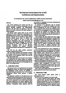
3 Test System Overall Architecture In this section, we describe the architecture of the present test system. First is a system block diagram, then a picture of the system with skins removed so its interior can be seen, then a picture of the high-speed subsystem card cage backplane, and finally a short description of the features that it contains.
DPS System Power HS Card Cage CPU AC Transformer Heat Exchanger
3.1 Test System Block Diagram Here is a simplified block diagram of the test system. PS1-5 Site 1
DUT-1
ADM APG / PND CPU
System Clocks CPU Bus
CNB
DPS SCAN Sequence Control ADM PS1-5 Site 2
DUT Clocks DUT-2
The system controller (CPU) above is simply a SUN ultra-SPARC. This provides ample power at nominal cost. The interface of this CPU to the rest of the system is contained on the CNB, which also has the system clock and DUT clock circuitry. Sequence control is implemented in 2 PCB’s identified as SCP and SCM (sequence control processor and memory). SCAN data are contained on several boards; as many boards are installed as required for the available scan chains. An Algorithmic Pattern Generator is implemented in two boards as well, APG and PND. All of the above capabilities are shared across two DUT sites; ADM assemblies distribute their data.
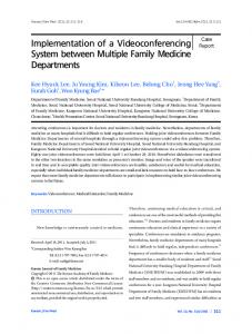
The box on the upper left contains the device power supplies (DPS) for two test sites. This box is conveniently suspended near a prober or handler, in order to minimize the power supply cable length. The inductance in a long power cable makes large current changes that are typical in scan-based structural tests of highperformance devices difficult to manage. The DPS subsystem is discussed briefly below. The entire test sytem, other than the DPS, resides in the cabinet as shown. The reduction in floor space required over previous ATE is obvious. 3.3 Test System Card Cage All the electronics for a dual-site test system are contained in a single card cage with 21 slots, shown below:
1 2 3 4 5 6 7 8 9 10 11 12 13 14 15 16 17 18 19 20 21
PS#5 (152 pin option) PS#4 PS#3 PS#2 PS#1 ADM SCP-ST SCM_ST CNB SCAN 1 SCAN 2 SCAN 3 SCAN 4 (152 pin option) APG (Memory DAT option) PND (Memory DAT option) ADM (2 site option) PS#1 (2 site option) PS#2 (2 site option) PS#3 (2 site option) PS#4 (2 site option) PS#5 (152p - 2 site option)
Each Pin Slice (PS in the figure above) contains the 16 MV of local memory, timing, formatting, and pin electronics for 32 DUT pins. Included also are independent levels generators and perpin PMU’s. Maximum pin count is 152 pins per site – which may seem a small number but is acceptable if either device pin count is small or there as an acceptable I/O test strategy for all pins not directly observed. It might seem strange at first glance that we found it appropriate to include per pin levels and per-pin PMU’s -- features normally associated with high-end functional testers -- in a costreduced structural test system. However, even on a structurally enabled device, the I/O pad drivers/receivers are fixed by their nature. Thus, some pins may be rail-rail CMOS, while others are GTL, etc. From a cost/flexibility standpoint, per pin levels were as costly as multiplexing a limited number of level DACs. The per-pin PMU's provide for the DC parametrics still required on a structural tester. Although they present a slight additional cost compared to a system PMU, they make up for it in faster test time. Each of the 3 (optionally 4) SCAN boards contains the scan memory and scan control for 12 chains of up to 512 MV per chain (which in the architecture easily expands to 1 GV per chain), so in this single cage there is room for a total of 24 GV of scan data. Scan memory is implemented using PC DIMM’s in order to keep
the cost of this subsystem as low as possible. The scan data are routed to both of the test sites simultaneously. The APG subsystem consists of APG and PND boards. Like the SCAN subsystem, the signals to and from the APG and PND boards access both sites simultaneously. 4 Key Features of the DFT Test System In this section, we describe briefly the reasoning leading to the unusual features of this system. 4.1 Dial-a-pipe DAT mode APG Typically, structural testers are expected to test memories by activating MBIST capability which is incorporated in the device. Very flexible, high-speed MBIST generators have been reported [9]. Such MBIST, however, still has a limited repertory of algorithms; provision for all algorithms which might surface any pattern sensitivity is today beyond the scope of MBIST technology. For this reason, it is valuable to provide optional APG capability. It is most effective if the APG can directly access the memory to be tested. This is termed DirectAccess Test (or DAT) mode. When many memory cores are incorporated in a device, the overhead of all the MBIST engines begins to add up. On the other hand, using one or a few engines for a large number of memories presents a routing challenge. Two issues must be addressed effectively in order to use an external APG on a number of memory cores. First, there will be a variety of different memory configurations, and providing the memory test patterns necessary for all of the possible pattern sensitivities over all of the memory configurations is time consuming. Far better to have a memory test library and a scaling mechanism that allows to apply library routines to specific memory sizes. Second, the memories scattered all over the device must be accessible from a variety of direct-access pins and at a variety of pipeline depths. The APG must be able to scale the patterns and adjust the pipelining to execute those tests efficiently. 4.2 Scan Pattern Linking Technology There is a large variety of different scan tests in today’s complex devices. Many cores will have canned scan patterns that must be managed by the scan test process. In this test system, a new approach to scan pattern management,
called Scan Pattern Linking, is introduced. The preprocessing necessary to create scan loads in current technology has been substantially reduced by the Scan Pattern Linking approach. In today’s technology, commonly scan data are computationally combined to form a monolithic scan load which is dumped to the tester. In the event that device or test debugging requires any kind of modification of the test, such as partial updates or changes to the order of application of the various tests, one must recompute the load module and reload it. In addition, if several cores share a chain, the scan data required to test one or another of those cores must be merged with other padding data, so the scan data module is contains merged information for a number of unrelated core elements. Each scan pattern created by the ATPG targets a specific set of fault locations in the circuit. Of course, for high volume manufacturing, we would like to organize the scan patterns such that we detect the largest number of existing defects as early as possible in the test. Unfortunately, we do not know, a-priori, which scan patterns will give us the best "bang-perbuck". Furthermore, with process tweaks, drifts and mask changes, the location for the highest incidence of defects will change. As a consequence, the effectiveness of each of the scan patterns will change with those changes. Scan pattern linking avoids the offline process of regenerating large monolithic scan loads. This allows the test engineer to reorder execution of the scan patterns dynamically, based on their actual, proven effectiveness. It also allows rapid, effective debug using scan patterns which are available and can be linked in immediately to isolate failing devices. Also, in order to manage the power in a complex device it is frequently advantageous to operate only a subset of the scan chains. So hardware which is capable of enabling some chains and then repeating the same scan sequence with other chains enabled, without stopping the test to reset the scan controller, saves test time and scan vector memory. Finally, whenever there is a need to repeat any portion of a scan chain as for initialization, the duplicate data required in scan memory expands the total memory requirement.
Far better not to waste time and memory by a more efficient approach to scan hardware. This approach is implemented using Scan Pattern Linking, where the scan hardware includes scan link tables which compose the scan data into the streams required for the device test without the computational overhead, the bulk memory, or the excessive load times. A related Scan Chain Linking scan data management strategy is described in detail by Jamie Cullen [11]. 4.3 Flexible Muxing Marker Generation ATE costs are frequently driven by relatively low volume custom components. High-performance functional ATE currently being delivered uses devices which contain several timing generator channels to achieve very high data rates on any given device pin. In order to implement a lowcost structural tester, and yet enable the later implementation of test systems with much higher data rates, the four-channel formatters of previous functional test ATE were redesigned to allow each such device to drive a wide range of different numbers of pins. The higher volume resulting from this flexibility will permit the delivery of both high-performance functional ATE at somewhat lower cost, and also enable less expensive structural ATE using the same devices. Sequencer-per-pin ATE drove the original development of these four-channel formatters. In order to achieve the desired 800 Megavector pattern rate, four timing "barrels" were created in a single device. Each barrel included a linear delay line implemented with a high-speed DAC and a fast comparator, and a timing marker pipe which conveyed to the output of the linear delay line the event type that the presented time value was to implement. Finally, the markers were all combined to provide the target data rate. For the structural test system, the required data rate was fully satisfied by a single barrel. As a result, these marker generators were redesigned with a new level of flexibility -- to be able to drive one, two, or four pins or, with external timed marker outputs for later merging, to be able to be combined in even larger groups for data rates of 1.6 GVPS, 3.2 GVPS, or more. There are two different types of marker generator, one for the drive side and one for the compare side. The drive side marker has eleven modes of operation. These modes of operation allow for application of the device in many types
of ATE; however, for implementing a low-cost structural tester the operating mode used is one in which four formatted data stream pairs are provided -- signals DHI[3:0] and DINH[3:0]. The two different signals are used to determine if the pin is to be driven high or not, or if it is to be inhibited or not. The compare side marker generator requires but three modes of operation -- one-pin, twopin, and four-pin modes. In the present tester, the operation uses the four-pin mode, where four pairs of signals ACH[3:0] and BCL[3:0] are received and strobed. 4.4 Pulse-Width-Modulated DPS
an external AC parametric capability on all I/O pins. This is obvious if not all pins are touched. It is almost as obvious if they are – today’s device speeds make at-speed functional test of the outputs a bit too costly for a low-cost primarily structural test system. So the way to mechanize functional test in this environment is to (a) drive the required subset of inputs for the functionality under study, (b) execute the clocking required for the functional state sequence under study at the desired speed, and (c) evaluate the final state of the device by any means available.
Power delivery to today’s highest-performance CMOS devices is becoming more and more challenging. Current requirements of up to 200 Amps in test mode are imminent. The surges of power characteristic of wide scan paths can produce current changes of many amps per ns. These current changes require very responsive DUT power supplies with low lead inductance.
The required subset of inputs may be nothing other than the clock, or it may be a data bus operating at a speed accessible to the tester (200 Mbps and below).
In order to provide this power, a new Device Power Supply assembly was developed. This system has the capability of delivering very large changes in current with minimal voltage aberrations. The power supply is contained in a separate power cage which can be located very close to the device fixture, allowing the impulse response to be delivered to the device without the traditional long lead inductance of current ATE.
Clearly, the third step above can normally use the device scan chains, so timed output strobes are not required for such limited functional tests – nor would DUT roundtrip time matter as much as in high-performance ATE. Equally clearly, if the device has no means of capturing and reporting the resulting activity, then the data collection is not possible.
Clocking mentioned in the second step might be managed either by the dedicated clock pins, or by an internal device PLL which is locked to it.
Most modern high-speed devices are driven by PLL-based internal clocks – with and without a PLL bypass mode of operation. The system incorporates a PLL-based DUT clock generator which provides four clock pins per site that can be used either as four single-ended clocks or two differential clocks. These clock pins are driven directly by a high-quality PLL with very small jitter. The period of these clocking pins is constrained by tester software to be exactly commensurate with the main tester pattern rate.
As noted above, the pin count per site is less – perhaps substantially less, than the number of pins which might be expected in a complex device. This is appropriate for a low-cost test solution provided there is a I/O loop or wrap test that establishes all device I/O’s function without direct touchdown. Such test strategies are not yet very common, but are becoming more popular. The argument for these strategies is quite sound: defects directly impacting device I/ O are relatively uncommon and are easily screened out at later stages in a distributed test approach. That they are uncommon matters in the sense that the cost of eliminating defects at any stage is inversely proportional to the defect density at that stage during individual device testing.
4.6 Functional Test Limitations
5 Conclusion
Delivering functional test in a structural tester is an interesting problem. The first limitation one must necessarily accept is that there will not be
The test system described here brings a variety of test resources and capabilities to the task of evaluating device structure to expose killer
This DPS cage also contains a number of supplies with higher voltages but lower currents. 4.5 Gated PLL-based DUT Clock Generator
defects. This allows for the development and application of several types of tests applied through the same device test port, which allows for economies of test development and fixturing as well as the overall economic benefit of a versatile, relatively low cost test vehicle. References [1] M.Abramovici, M.A.Breuer, and A.D.Friedman, "Digital Systems Testing and Testable Design", IEEE Press, Piscataway, New Jersey (1994) [2] E. B. Eichelberger and T. W. Williams, "A Logic Design Structure for LSI Testability", J. Des. Auto. Fault-Tolerant Computing, Vol 2, pp 165-178 (May, 1978) [4] K.S.Kim et. al., “DPDAT: Data Path Direct Access Testing”, ITC Proceedings (2001) [5] H.Petroski, To Engineer is Human: The Role of Failure in Engineering Design, Vintage Books (1992) [6] P.Maxwell. et al, "The Effectiveness of IDDQ, Functional, and Scan Tests: How Many Fault Coverages Do We Need?", ITC Proceedings, pp 168-177 (1992) [7] P.Nigh, et al; "An Experimental Study Comparing the Effectiveness of Functional, Scan, IDDQ, and Delay Fault Testing", IEEE VLSI Test Symposium Proceedings, pp 459-464 (1997) [8] P.Nigh and A.Gattiker; “Test Method Evaluation Experiments and Data”, ITC Proceedings, pp 454-463 (2000) [9] S.Nakahara et. al., “Built-in Self Test for GHz Embedded SRAMs Using Flexible Pattern Generator and New Repair Algorithm”, ITC Proceedings, pp 301-310 (1999) [10] B.G.West, "At-Speed Structural Test", ITC Proceedings, pp (1999) [11] J.Cullen, "Flexible Scan Operation using Scan Link Tables", ITC Proceedings (2001)