Architecture of a Power-Gated Wireless Sensor Node
Recommend Documents
Sep 30, 2013 - Department of Architectural Engineering, Yonsei University, 134 Shinchon-dong, Seoul 110-732, ... during non-measurement and non-transfer periods. ..... element) to the displacement of the free end of the mega-trusses .... Lynch, J.P.
AbstractâWireless sensor networks are widely used in data gathering applications from the environmental to the health care system. This type of networks ...
explores the WSN architecture according to the OSI model with some protocols in
order to achieve good background on the wireless sensor networks and help ...
good choice for a battery-limited device likes sensor node. This paper ... Index TermsâWireless sensor network, Dynami
microsystem designed to be part of a wireless sensor network. This microsystem ... several advantages allowing a global decrease in the power consumption of ...
Key words: power harvesting, environmental monitoring, sensor networks, ... a multiparametric smart sensor node (SENNO) dedicated to air quality monitoring systems. 2. .... Six high-performance thermoelectric generators (TEGs) (see Fig.
based security for protection against breach of systems and data integrity. .... core and therefore promise an extra degree of security over a software only ...
Gerardine Immaculate Mary2. Asst. Prof. (Sr.), School of Electronics Engineering. VIT University, Vellore, Pin: 632014, India. Abstract: Judicious deployment of ...
a multiparametric smart sensor node (SENNO) dedicated to air quality monitoring ..... that the law of the recovered energy (in μW) from 3 W EIRP power at 915 ...
intelligently manages energy transfer for perpetual operation without human ..... stacked to a window in the case where differences between external ambient ... draw is very low, but where periodic pulses of higher load current may be required ...
Oct 24, 2016 - AbstractâWe investigate the secure connectivity of wireless sensor networks ...... Press, 2001, cambridge Books Online. [Online]. Available:.
School of Mechanical and Systems Engineering, Newcastle University, UK ... powered (or take advantage of nearby power supply if available) sensor nodes, each ... connected to a wireless sensor node for the wireless transmission of ..... Similarly, th
sensor node should be small size, low power consumption and low cost. ... Researchers have developed a scalable android application based on a smartphone to diagnose ... operating machinery in a factory zone using smart phones [10].
family,â (http://www.ti.com/lit/ds/symlink/msp430f1611.pdf), 2013, last access March ... cation of a wireless sensor networks and web2py architecture for factory.
Characterization. W500 Lenovo laptop .... the scavenger which best encompasses all of the above considerations is a trapezoid (figures 2 and 3). The widened ...
Maximum Power Point Tracker is required, as is the capability to recharge
secondary .... The C-code and LabVIEW VI they provided allowed ..... Implement
a DC/DC Converter that regulates current through Pulse Frequency Modulation
to.
May 16, 2012 - This is an open access article distributed under the Creative Commons ... nology, wireless sensor networks technology is widely used in many ...
wireless sensor module in classrooms and faculty cabins. The cost is ..... Since cabins were open on top, two split Air Conditioners of cooling efficiency of 1.5.
Yuvraj et. al have proposed a WSN for detecting the occupancy to control ..... We wish to thank Mr. Manish Shekhar, Mr. Navin Singh and Mr. Saurabh Sinha,.
A Wireless Sensor Networks (WSN) is now widely used in precision agriculture applications. ... applications that traditional technologies could not address. .... being that changes in pH modulate the drain current of the device [12, 13, and 14]. 2.
A Wireless Sensor Networks (WSN) is now widely used in precision agriculture applications. ... applications that traditional technologies could not address.
sensor network. It includes an embedded processor, memory, a CMOS image sensor, image acquisition unit, RF module and power unit etc. Power-efficient.
In Wireless Sensor Networks (WSN), sensor node deployment is essential for ... But the existing optimization solution suffers from limited energy storage, node death, ... the mobile sensor nodes should cover the entire monitoring environment.
Jul 6, 2014 - e-mail: [email protected]. H. A. Omar e-mail: ... The special characteristics of wireless sensor network (WSN) allow them to be ... sensors monitor and report the locations of moving objects within the network ...
Architecture of a Power-Gated Wireless Sensor Node
They create a power gating ... requirements, the SNOC designer may add optional ... Header. Footer. 846. Authorized licensed use limited to: Rolf Kraemer.
11th EUROMICRO CONFERENCE on DIGITAL SYSTEM DESIGN Architectures, Methods and Tools
Architecture of a Power-Gated Wireless Sensor Node Goran Panić, Daniel Dietterle and Zoran Stamenković IHP GmbH, 15236 Frankfurt (Oder), Germany {panic, dietterle, stamenko}@ihp-microelectronics.com
effective in WSN nodes operating at a very low duty cycle where cutting the power of inactive functional blocks leads to significant power savings. Power gating technique suggests the implementation of power gates in order to switch off the leakage currents of inactive functional blocks. This technique is primarily seen as a low power option for the emerging multi threshold CMOS (MTCMOS) technology. It uses the high-threshold-voltage (highVth) transistors to isolate the low-threshold-voltage (low-Vth) circuits from the power and ground lines. Therefore, we have decided for power gating as the main power saving leverage in wireless sensor nodes and propose a novel architecture of the sensor node, which includes a power gating controller and a sophisticated functional-block power gating mechanism. The paper starts with discussion on dynamic and static power contributions to the total power consumption of a sensor node (Section 2). Section 3 describes details of the power gating mechanism. Section 4 presents the proposed sensor node architecture. Section 5 concludes the paper.
Abstract In this paper we investigate the benefits of power gating in wireless sensor nodes operating at a very low duty cycle. It is shown that the static power loss in such a node is significant portion of the total power consumption. Therefore, we have defined power-gated wireless sensor node architecture and developed a power gating mechanism to reduce the static power loss of its functional blocks. The new node architecture, its components and power gating mechanism are described in detail.
1. Introduction Wireless sensor networks (WSN) consist of a large number of wireless sensor nodes deployed randomly in the area. The nodes collect the environmental data and send them through the network towards the sink node. The sensor networks are constructed to be operational for a long time without replacing the batteries. Therefore, power is considered to be the most important constraint in all aspects of WSN design. Minimizing the total power needed to transfer the data from a leaf node to the sink is the primary task of WSN design. The most of questions arise on network level. Depending on a specific application, different network topologies and corresponding MAC (media access control) [1] and routing protocols have been investigated [2]. The problems of data dissemination and data aggregation are strongly power related and therefore receive a lot of attention [3]. The proposed hardware solutions include novel node architectures that utilize optimized radio and digital parts [4]. The energy harvesting is also considered as a feasible solution to extend the battery life [5]. The two most promising non-standard approaches to power saving within a sensor node are the dynamic voltage/frequency scaling [6] and power gating [7]. While the first is considered as a promising solution for high performance WSN nodes, the second is mostly
2. Dynamic Vs Static Power in Sensor Node The design requirements of a sensor node are typical to all portable and battery powered devices. The main target is to reach maximum performance at minimum power. Since the leakage contribution increases with every new generation of CMOS technology [8], the power optimization has to consider both the static and the dynamic power. 2.1. Dynamic Power The dynamic power is consumed during the active mode of operation. It depends on the supply voltage and applied clock frequency and is linear to the activity factor of a circuit. Reducing one of those parameters will reduce the dynamic power. The common practice
844
Authorized licensed use limited to: Rolf Kraemer. Downloaded on November 17, 2008 at 04:28 from IEEE Xplore. Restrictions apply.
to reduce the dynamic power is to apply the clock gating of inactive blocks. Clock gating turns clocks off when they are not needed and thus prevents undesired toggling in the distribution network of the clock.
3. Power Gating Mechanism Power gating is a design technique used to reduce the overall static power loss of a chip [9]. Compared to the clock gating used to reduce dynamic power, the power gating is more invasive since it affects interblock communication. It adds significant delays and needs a block isolation technique that secures the proper system functionality.
2.2. Static Power The static power is the power loss due to leakage currents in the circuit. The most important leakage sources are the subthreshold leakage and leakage through the oxide. The latter depends on the oxide thickness and the supply voltage. Once the high-k dielectrics reach the mainstream production, this source of leakage will be significantly reduced. The subthreshold leakage depends on the threshold voltage Vth and the supply voltage Vdd. Increase of Vth or reduction of Vdd will reduce the leakage. The leakage is present in the circuit whenever the power supply is on. The contribution of leakage depends on the applied CMOS technology and the duty cycle of a node. The more time a circuit spends in idle mode, the higher is the leakage contribution. The straightforward method to reduce the leakage during idle periods is to switch off the idle circuit from the power supply.
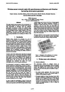
3.1. Component Activity Profiles The efficiency of power gating depends on the activity profile of a component. Generally, the component’s activity consists of subsequent active and idle periods. Figure 1 shows an example of the activity profile when only the clock gating is applied. The active and idle periods are initiated by the corresponding WAKE and SLEEP signals. SLEEP
Power
2.3. Total Power
10mW
t
i
and
Dynamic Power
Dynamic Power
Activity 1
Activity 2
Activity 3
Static Power Activity 1
SLEEP
i
off
Pi represent dynamic and static
Static Power (e.g. Clock Gated)
Static Power
Static Power
WAKE
SLEEP
WAKE
SLEEP
200mW
power of the i-th component, Ed and Es are dynamic and static energy consumed by a sensor node; t = t ion + t ioff is the sensor node lifetime. Most
Power
applications see sensor nodes as very low duty cycle