are efficient filter structures for sample rate conversion with factors of two. The proposed transformation reduces the sam- ple period bound with up to 33% for ...
ARITHMETIC TRANSFORMATIONS FOR INCREASED MAXIMAL SAMPLE RATE OF BIT-PARALLEL BIRECIPROCAL LATTICE WAVE DIGITAL FILTERS Henrik Ohlsson, Oscar Gustafsson, and Lars Wanhammar Department of Electrical Engineering, Linköping University, SE-581 83 Linköping, Sweden E-mail: {henriko, oscarg, larsw}@isy.liu.se
ABSTRACT In this paper we propose an arithmetic transformation of firstorder allpass lattice wave digital filter sections implemented with bit-parallel, carry-save arithmetic which increases the maximum sample rate. Such filter sections are the critical component of bireciprocal lattice wave digital filters which are efficient filter structures for sample rate conversion with factors of two. The proposed transformation reduces the sample period bound with up to 33% for CSDC coefficients. This is obtained with a coefficient with four nonzero bits, and, dependent on the value of the adaptor coefficient, at the expense of up to 28% more carry-save adders. An example is presented where an adaptor with a coefficient with two nonzero bits is implemented. This results in a reduction of the sample period bound with 25% with a 14% increase of the number of carry-save adders needed.
1. INTRODUCTION Bireciprocal lattice wave digital filters (BLWDFs), or halfband filters, is a class of digital filters suitable for efficient implementation of interpolators and decimators for sample rate conversion with factors of two using the polyphase representation of the transfer function [1]. This results in a structure where all filtering may be performed at the lower sample rate. Compared to FIR filters, BLWDFs have a low arithmetic complexity which yield low power consumption and low chip area. However, since BLWDFs are recursive structures there is a bound on the maximal sample rate [2]. Thus, to use BLWDFs in high speed applications this bound should be increased. Also, any excess speed obtained can be traded for reduced power consumption through power supply voltage scaling [3]. A first-order allpass lattice wave digital filter section, which is the limiting recursive component in a BLWDF, is shown in Fig. 1 where the loop limiting the sample rate is indicated. For a polyphase representation of the BLWDF for interpolation and decimation we only have to consider filter sections with one delay element in the recursive loop though there are two delay elements in the original structure. The maximal sample rate is determined by the latency of the operations in the loop divided by the number of delay elements in the loop. For the first-order lattice wave digital filter section the minimum sample period, Tmin, is 2T add + T mult T min = ----------------------------------1
(1)
T
T
a a
x(n) y(n)
x(n)
y(n)
Figure 1. Sample rate bound for first-order filter section with a symmetric two-port adaptor. where Tadd is the latency for an addition and Tmult is the latency for a multiplication. The main contributor to this bound is Tmult. For a bit-parallel implementation the latency of the multiplication depends on the number of partial products to be added. Each partial product is generated by a nonzero bit in the coefficient. Thus, to reduce Tmin for a bit-parallel implementation, the number of nonzero bits in the coefficient word should be as low as possible. This is obtained for CSDC coefficients. The average number of nonzero bits in a CSDC number is approximately Wcoeff/3 where Wcoeff is the coefficient word length, compared to Wcoeff/2 for the binary representation. Thus, CSDC representation yields a significant reduction of the number of nonzero bits in a coefficient [4]. One method for reducing the number of nonzero bits in the coefficient further is to cascade several filters and thereby reduce the stopband requirement on each filter stage [5]. This results in shorter coefficient word lengths for each filter stage which yields a reduced number of nonzero bits. Efficient cascaded polyphase structures for decimation and interpolation where the filtering is performed at the lower sample rate have been proposed in [6]. The sample period bound may be reduced even further by arithmetic transformations of the filter structure. In [7] some transformation performed on a bit-serial first-order lattice wave digital filter structure that reduces the latency of the critical loop with one addition is presented. In this paper similar arithmetic transformations are applied on such filter structures implemented with bit-parallel arithmetic.
2. CARRY-SAVE IMPLEMENTATION Carry-save arithmetic, which is a redundant arithmetic, is efficient for implementation of many DSP algorithms since time consuming carry propagation may be avoided [8]. One such case, where carry-save arithmetic is especially efficient, is the implementation of wave digital filters [9]. The use of
carry-save adders (CSAs) instead of carry-propagation adders reduces the latency for the computations in the loop significantly. A CSA adds three operands and yields as result a sum vector and a carry vector. The latency for a CSA is equal to the latency of one full adder. CSAs can be combined into adder trees which are efficient for adding several operands with a low overall latency. This is efficient for implementation of multiplications where several number of partial products need to be added. A tree with a minimum height is the Wallace tree [10]. A drawback with the Wallace tree is that it yields an irregular routing, which has a number of drawbacks, e.g., irregular wire routing, which causes different loads on the full adders and glitching which contributes to large power consumption. Instead an overturned-stair adder tree may be used. Such a tree has a regular routing and has the same height as a Wallace tree when adding up to 18 inputs [11]. The latency for a multiplier based on a Wallace tree is dependent on the height of the adder tree, i.e., the number of partial products in the coefficient. The latency for such multipliers can therefore be expressed as a number of Tadd. To complete a multiplication implemented with carry-save arithmetic a vector merging adder (VMA) is needed at the output of the adder tree to merge the sum and the carry vector. However, when implementing the symmetric two-port adaptor with CSAs, the VMA can be placed outside the recursive loop, at the nonrecursive output of the adaptor. Hence, no carry propagation is required in the recursive part and Tmin can be expressed as a number of Tadd. It is also possible to pipeline the VMA to reach Tmin. However, implementing the adaptor with CSAs means that the data inside the adaptor is represented with two data vectors. This makes it difficult to identify if an overflow occurs. Overflow detection and correction is necessary in order to guarantee overflow stability for wave digital filters [12]. In [13] a scheme for detection and correction of overflows that guarantee the stability in carrysave implementation of WDFs was introduced. Another difference between a carry-propagation implementation and a carry-save implementation is the possible occurrence of carry overflows. When performing a carry-save addition there is a possibility for an error to occur in the final sum due to the discarding of carry bits. A solution for this has been proposed in [8] where the full adder used for the most significant bits of each CSA can be modified to correct any possible errors in the carry bits. This can be done without introduction of any extra delay in the full adder.
3. PROPOSED IMPLEMENTATION The symmetric two-port adaptor used in the first order allpass section and shown in Fig. 1 is described with the following equations B1 = α ( A2 – A1 ) + A2
(2)
B2 = α ( A2 – A1 ) + A1
(3)
T T
>>2 -
>>2
x(n)
y(n)
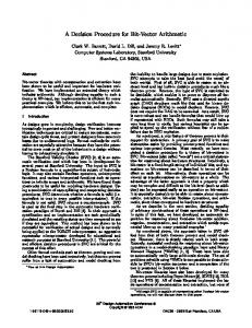
Figure 2. CSA implementation of the original structure for α = −0.75. Implementation of the adaptor with carry-save arithmetic using these equation yields a structure as shown in Fig. 2, where α = −0.75 = −1.01CSDC. From this figure we also see that the operations in the critical path consists of two carry-save adders and a Wallace tree for the multiplication. In this example we obtain a Tmin of 4Tadd. One method to reduce the latency for the critical loop would be to combine all additions in the loop into one Wallace tree. This is possible by rewriting (2) and (3) as B 1 = ( 1 + α ) A 2 – αA 1
(4)
B2 = ( 1 – α ) A1 + α A2
(5)
This is a numerically equivalent representation of the adaptor. Thus, the method used for detection and suppression of overflows in a carry-save WDF previously discussed is still valid. The reordering of the arithmetic operations and the quantization operation in the adaptor corresponding to (4) and (5) is shown in Fig. 3. When implementing the transformed adaptor using carry-save arithmetic Tmin may be reduced with up to two Tadd. The cost for the 1-α multiplication depends on the number of nonzero bits in the 1-α coefficient. This number is, depending on the value of α, either equal, one more, or one less than the number of nonzero bits in α. In Fig. 4 the same filter section as in Fig. 2 has been implemented using the proposed structure. In this example, where we have two nonzero bits in the coefficient, we need to increase the height of the adder tree for the α multiplication with one to add the result from the 1-α multiplication. Thus, for this example, Tmin is reduced with one Tadd to 3Tadd compared to the original structure. In this case there is no need for a VMA in the 1-α multiplication since there are two inputs available in the adder tree in the loop. The number of carry save adders used for the proposed structure is seven compared to six for the original structure. Thus, a reduction of Tmin with 25% is obtained with a 14% increase of the number of CSAs for α = −0.75.
T
A2
a
B2
Q
-
A2
B2
Q
a
Number of nonzero bits in coefficient
Original
Proposed (without input VMA)
Proposed (with input VMA)
1
2
1
1
2
4
3
3
3
5
4
4
4
6
5
4
5
7
5
5
6
7
6
5
7
8
6
6
-a
Q
Q
B1
A1 T
A2
T
B2
a
B1
A1 A2
T
B2
a
Q
Q 1- a
-a
-
-
Q
A1
B1
A1
8
8
6
6
Q
9
8
7
6
B1
10
9
7
7
Figure 3. Reordering of operations in a first-order filter section.
Table 1. Comparison of Tmin (in Tadd) between the original and the proposed structure.
T
Number of nonzero bits Original in coefficient
T
>>2
-
Proposed 2 --- < α < 1 3
-
Proposed 2 – 1 ≤ α < – --- , 3 2 1 --- < α < --3 3
Proposed 1 2 – --- < α < --3 3
1
4
4
5
6
2
6
6
7
8
3
8
9
10
11
4
10
12
13
14
5
12
15
16
17
Figure 4. CSA implementation of the proposed structure for α = −0.75.
6
14
18
19
20
7
16
21
22
23
4. RESULTS
8
18
24
25
26
The proposed structure for implementation of first-order allpass LWDF sections has been evaluated for the number of carry-save adders needed and for the difference in Tmin for different CSDC coefficients. The evaluation presented in this paper considers CSDC coefficients with up to 10 nonzero bits. With 10 nonzero bits in the CSDC coefficient, all coefficients with word lengths of up to 19 bits can be represented. Table 1 presents Tmin for both the original structure and for the proposed structure. The later has been evaluated both with and without a vector merging adder at the output of the 1-α multiplication. This only makes a difference when we have four, six or nine nonzero bits in the coefficient. This is because the Wallace tree for the α multiplication for such α has one free input only and the height of the adder tree for the multiplication must then be increased by one if there are two extra inputs in the adder tree. In Table 2 the number of carry-save adders needed for the original and for the proposed structure is compiled. The number of CSAs needed gives an estimation of the extra hard-
9
20
27
28
29
10
22
30
31
32
>>2 >>2