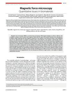
PHYSICAL REVIEW B 78, 113401 共2008兲
Atomically resolved force microscopy images of complex surface unit cells: Ultrathin alumina film on NiAl(110) G. H. Simon, T. König, M. Nilius, H.-P. Rust, M. Heyde,* and H.-J. Freund Fritz-Haber-Institut der Max-Planck-Gesellschaft, Faradayweg 4-6, D-14195 Berlin, Germany 共Received 10 July 2008; published 2 September 2008兲 In this Brief Report we present atomically resolved images of the ultrathin alumina film on NiAl共110兲. For the first time detailed images of the complex microstructure for both reflection domains have been obtained by frequency modulation dynamic force microscopy using a very stable, custom built, dual mode scanning force and scanning tunneling microscope. Measurements have been performed under ultrahigh vacuum conditions at 5 K with a quartz tuning fork as a force sensor. The high spatial resolution allows to derive 28 atomic positions in real space in the surface unit cell by simple graphical analysis. This has been successful without application of filtering or correlation methods, emphasizing the potential of this force microscopy method on complex oxide surfaces. With respect to topographic height even quantitative agreement with theory could be achieved, here shown for selected structural elements within the unit cell. Furthermore, deeper insight into a wavelike morphological feature could be obtained. Consistency with a published density-functional theory model and connections to other data from the literature are discussed. DOI: 10.1103/PhysRevB.78.113401
PACS number共s兲: 68.47.Gh, 77.55.⫹f, 68.55.⫺a, 68.37.Ps
Ultrathin alumina overlayers on certain low index faces of metal or alloy single crystals, originally developed to mimic properties of bulk aluminum oxide in surface studies, where charging hampered analysis with electron techniques, have long become a research field in their own right. This is still due to the full set of electron analysis techniques applied to them, but besides this the thin films can be linked to technological problems regarding interfaces and insulating interlayers in miniaturized electronic and magnetic devices as well as protective coatings and heterogeneous catalysis. Of academic interest are fundamental physical and chemical properties of these wide band-gap insulators, in particular the relation between structure and functions such as adsorption as well as transport and interface properties. One example for such a film is the 5 Å thin ordered alumina overlayer which can be grown by selective oxidation on 共110兲 surfaces 共CsCl structure兲 of the ordered intermetallic NiAl.1 Despite its large band gap of about 6.7 eV2 it allows electron flow due to its limited thickness. Thorough low-energy electron diffraction 共LEED兲, photoemission spectroscopy, Auger electron spectroscopy, electron-energy-loss spectroscopy, angle-resolved ultraviolet photoelectron spectroscopy, ion scattering spectroscopy, and scanning tunneling microscopy 共STM兲 and scanning tunneling spectroscopy studies1–10 have been performed in the framework of model catalysis over the last two decades. Together with a recent STM and density-functional theory 共DFT兲 study this led to an atomistic model of the film that matches many of the experimental findings.11 The accumulated data on this film in the literature give so far evidence for a two double-layer structure free of nickel with alternating aluminum and oxygen layers. It is oxygen terminated toward the vacuum with the next lower aluminum layer being on average relaxed inwards by about 40 pm. The lattice constants as determined by LEED are b1 = 10.55 Å and b2 = 17.88 Å enclosing an angle ␣ = 88.7°. Each oxide surface unit cell covers 16 of the 2.89⫻ 4.08 Å2 sized rectangular NiAl共110兲 surface unit cells. Dimensions, geometry, and orientation between the oxides’ two reflection domains and the substrate are illustrated in Figs. 1 and 2共c兲. However, due to 1098-0121/2008/78共11兲/113401共4兲
technical constraints, the DFT model11 assumes a commensurate structure 共10.93 Å, 17.90 Å; ␣ = 88.16°兲 for the film which is incommensurate in the 关001兴 direction of the NiAl substrate. Furthermore the underlying STM data for the topmost oxygen layer have been obtained under extreme tunneling conditions giving rise to speculations over substrate influence, mixed contributions from several layers, and force interactions in the images. Therefore the atomic surface structure is still under discussion and more real-space information with atomic resolution is still desirable. Frequency modulation dynamic force microscopy 共FM-DFM兲12 has been significantly improved over the last ten years and atomic resolution has been obtained on metal, semiconductor, and insulator surfaces.13–16 The amount of data obtained from large and complex surface unit cells of wide band-gap oxides, however, is still very limited. Recent work on bulk alumina or associated thin films on NiAl and Ni3Al surfaces has been promising though.17–21 Hence the large parallelogram shaped surface unit cells of the alumina film on NiAl共110兲 can be considered the acid test for the resolution of ultrahigh vacuum 共UHV兲, low-temperature FMDFM. Here the progress on thin films is considered a stepping stone on the way to resolving all positions in large complex reconstructed surface unit cells of bulk insulators. a
b
FIG. 1. High-resolution FM-DFM images of the ultrathin alumina film on NiAl共110兲. 共a兲 Domain B; 共b兲 domain A. The geometric relation between the oxide and the small NiAl共110兲 surface unit cell is illustrated. Atomic positions are marked with crosses. Scan area 3 ⫻ 3 nm2 each. 共a兲 ⌬f = −6.2 Hz, AOSC = 1.4 Å; 共b兲 ⌬f = −6.7 Hz, AOSC = 1.7 Å.
113401-1
©2008 The American Physical Society
PHYSICAL REVIEW B 78, 113401 共2008兲
BRIEF REPORTS a
b
c
NiAl(110)
B
d
[11 0]
b2
A
]
01
[0
a b1
e
f
FIG. 2. 共a兲 Stack of ten superimposed overlays with crosses of the surface unit cell taken from Fig. 1共a兲 of domain B. The spread in each set of crosses indicates the uncertainty due to imaging noise, weak contrast, and reading errors. 共b兲 Average overlay as determined from 共a兲 giving the mean positions of the groups of crosses. 共c兲 Geometry and dimensions of the two oxide overlayer domains A and B, their orientation relative to each other and to the NiAl共110兲 substrate 共b1 = 10.55 Å, b2 = 17.88 Å, ␣ = 88.7°兲. 共d兲 Average positions of domain A 共crosses兲 reflected onto result for domain B 关circles from 共b兲兴 for comparison. 共e兲 Positions from the averaged overlays of four independent images 共domain B兲. The spread here allows to check reproducibility. 共f兲 Average of positions from 共e兲.
We present for the first time FM-DFM images of all 28 individual surface oxygen positions in the surface unit cells of both reflection domains of the ultrathin alumina film on NiAl共110兲. The custom-built microscope setup is designed for UHV and liquid-helium temperature 共5 K兲 operation.22–24 The sensor used for the present study has been a quartz tuning fork as presented in Ref. 25 with a cut Pt90Ir10 wire as a FM-DFM/STM tip. The tuning fork assembly and electronics in use are capable of simultaneous recording of tunneling current IT and frequency shift ⌬f while controlling the z position of the tip via either of them.24 Force sensor parameters are k = 22 000 Nm−1, f 0 = 17.700 kHz, the oscillation amplitude AOSC has been set to values within the range 1.4– 1.8 Å. Here images have been recorded in the constant oscillation amplitude FM-DFM mode with constant ⌬f. Alumina preparation has been carried out according to the recipe presented in the literature.1,8 The prepared film exhibited the usual flat topography, the well-known long-range order on extended terraces and reflection as well as antiphase domain boundaries. During this study several atomically resolved FM-DFM images of both of the film’s surface unit cells have been obtained with previously unparalleled resolution 共Fig. 1兲. Please note that the postproduction of the images consisted
of leveling 共subtraction of a parabola兲 only. No further filtering has been necessary. However, minor lateral corrections had to be performed to account for slight drift, due to long acquisition times. Images have been recorded on different areas of one surface preparation. Several changes in the nanoscale tip geometry took place, mostly due to in situ preparation of the tip by field emission and/or controlled dipping into and pulling of necks from the sample surface. Therefore it has to be shown that images before and after tip changes reproducibly show the same structure within the surface unit cell. The images have been evaluated with respect to bright protrusions. After identification of a corresponding surface unit cell in all images of both domains, overlays of the observed protrusions with crosses have been made and compared by stacking overlays from different images 共Fig. 2兲. A series of overlays for the same image gives a measure for the statistical reading error and uncertainty due to noise. A series of overlays from different images 共after a tip change and/or on a different site兲 gives an idea of the contribution of imaging conditions, i.e., scanning parameters, shape, and atomic composition of the tip as well as atomic contrast mechanisms, to the uncertainty in position. A recurrent structure from different images is therefore a measure for reproducibility. The average positions in both cases are the mean positions of the sets of crosses belonging to individual positions in different overlays. Average overlays are shown in Figs. 2共b兲, 2共d兲, and 2共f兲. The result is only reasonable if the reading error does not lead to overlapping positions in different overlays from one image and if averaged overlays from A and B domains reflected onto another are sufficiently similar. The rather regular shapes of the areas covered by the groups of crosses belonging to the individual 共and averaged兲 positions in different images emphasize that the found overlays are quite well defined 关dashed ellipses in Figs. 2共e兲 and 2共f兲兴. Most of the positions can be distinguished without any doubt. As the evaluated images, which have been recorded with different microscopic tips on different surface sites, show equal patterns, reproducibility is established. This is supported by the finding that the structure in one domain is reproduced by the mirrored positions from the other reflection domain 关Fig. 2共d兲兴. Consistency is acceptable and one can distinguish all positions clearly. Each surface unit cell contains 28 observable protrusions matching the number of atoms proposed for the topmost oxygen layer by the DFT model,11 as compared to only 24 atoms of the topmost aluminum layer. Figure 3 shows a direct graphical comparison with that oxygen layer of the model given in the supplement to Ref. 11. We find the similarity rather striking. In first approximation the sites marked with crosses in Fig. 1 indicate individual oxygen positions. One can also see that positions interconnecting the characteristic squares and rectangles of eight oxygen sites in the model are among the brightest protrusions in the FM-DFM images. On the other hand, protrusions at points with lower contrast naturally exhibit larger scattering of the crosses in Fig. 2共e兲. Therefore much more effort has to be made to pin deviations which might exist between model and structure. Less defined points fall into the troughs of the wavelike feature visible in FMDFM images 共Figs. 1 and 4兲. It consists of alternating bright and dark rows—crests and troughs. This wavelike topogra-
113401-2
PHYSICAL REVIEW B 78, 113401 共2008兲 a
b
1 2 3 4
ΔzEXP (pm)
b 40
FIG. 3. Comparison of the atomic positions of the averaged surface unit cells for both domains 共crosses兲 with those of the topmost oxygen 共gray dots兲 and aluminum 共black dots兲 atoms in the DFT model 共Ref. 11兲. The dashed and solid gray lines indicate the surface unit cell position and rectangular blocks of eight oxygen atoms from Ref. 11, respectively. 共a兲 Domain B; 共b兲 domain A.
profi
les C
B
322
C
D
A
1
B
3 2 Profile Length (nm)
D
4 0
A 10
5 0 -5 -10 ΔzEXP (pm)
FIG. 4. FM-DFM image of a B domain 共scan range 4.1 ⫻ 4.8 nm2, ⌬f = −5.5 Hz, A = 1.4 Å兲. The wavelike topographic feature of the oxide film exhibits two inequivalent but equidistant crests. They differ in the arrangement, contrast, and number of their brightest protrusions. The length of a complete period of the feature is 18 Å. The right part shows an average of 322 line profiles 共gray curve兲 lined up along the short end 共indicated by the dashed double arrow line兲 of the three unit cells broad rectangle marked in the image. The black curve has been smoothed. Every second crest is less pronounced. The dashed and solid line segments in the line profile are set to spacings of a quarter of a unit cell length.
2
560
8
7
540
20 0
520
4
-20 0.0 c 40
5
6 0.2
E
ΔzEXP (pm)
phy of the surface unit cells is in fact typical for the film26 and related to stress and commensurability.27,28 As observed by FM-DFM before,18 the crests have a distance of 9 Å but the full repeat unit has a length of 18 Å, i.e., that of an oxide unit cell. Each two of the protruding rows differ slightly in apparent structure, height, and contrast making them inequivalent as shown in Fig. 4. However a row pairing in lateral direction could not be confirmed. One finds those wave crests pronounced where rectangular arrangements of eight oxygen positions are nearly aligned with the 关001兴 direction of the NiAl substrate. This relates to earlier findings regarding the alignment of adsorbed gold atoms along this direction.29 Therefore the inequivalence of the crests can be seen as a manifestation not only of strain but also of the influence of the substrate onto the film surface. As lateral resolution allows direct identification of individual structural units, the topography of the characteristic rectangular arrangements of eight oxygen atoms has been evaluated in detail 共Fig. 5兲. From the images it can be seen
1
5 E F 6 G A H 7 B C 8 D
0.4
F
3 0.6
500 0.8
1.0
D
C
520
0
-20 0.0
560 540
20
A 0.2
B
zDFT (pm)
a
G
0.4 0.6 0.8 Profile Length (nm)
zDFT (pm)
BRIEF REPORTS
H 1.0
500
FIG. 5. 共a兲 Topography image of rectangular blocks of eight protrusions labeled with 1–8 and A–H, respectively; domain A. Each two parallel rows of four positions 共dashed lines兲 are inclined in opposite directions along the long side of each rectangular block. Scan range 2.5⫻ 1.6 nm2, ⌬f = −6.7 Hz, AOSC = 1.7 Å. 共b兲–共c兲 Line profiles along dashed lines from 共a兲 in comparison to calculated absolute heights for corresponding oxygen positions from the DFT model 共boxed crosses兲. Please note that this figure shows individual line profiles giving rise to a larger scale range in z direction as compared to the average profile given in Fig. 4.
that each two parallel rows of four protrusions are contrarily inclined with respect to each other. This is shown in Fig. 5 and compared to height values for the calculated oxygen sites. The experimental line profiles are in reasonable qualitative and quantitative agreement with the theoretical result. In conclusion FM-DFM has been used to obtain atomically resolved images of the complex surface unit cells of the ultrathin alumina film on NiAl共110兲 to derive the atomic microstructure of its topmost oxygen layer. For the first time it has been possible to observe all individual atomic positions in the surface unit cells 共both reflection domains兲 of that layer by FM-DFM unambiguously. Our results confirm the combined STM and DFT model11 and complement earlier FM-DFM images18 from the literature. Our experiments demonstrate the enormous potential of FM-DFM measurements. For selected structural elements quantitative agreement with DFT has been found for the topographic height. Resolved details of the film’s wavelike morphological feature and analysis of the atomic corrugation point toward interactions between film surface and substrate. Graphical evaluation of the images and line profiles from the surface unit cells has been sufficient to derive the positions. No application of any filtering or correlation techniques has been necessary. The results are a promising step toward real-space atomistic surface characterization of thick insulating films and eventually bulk surfaces of wide band-gap insulators with complex surface unit cells. The authors wish to thank Thomas P. Pearl for a critical review of the manuscript and helpful suggestions.
113401-3
PHYSICAL REVIEW B 78, 113401 共2008兲
BRIEF REPORTS 15
*
[email protected] 1 R.
M. Jaeger, H. Kuhlenbeck, H.-J. Freund, M. Wuttig, W. Hoffmann, R. Franchy, and H. Ibach, Surf. Sci. 259, 235 共1991兲. 2 S. Andersson et al., Surf. Sci. 442, L964 共1999兲. 3 H. Isern and G. R. Castro, Surf. Sci. 211-212, 865 共1989兲. 4 J.-P. Jacobs, S. Reijne, R. J. M. Elfrink, S. N. Mikhailov, H. H. Brogersma, and M. Wuttig, J. Vac. Sci. Technol. A 12, 2308 共1994兲. 5 J. Libuda, F. Winkelmann, M. Bäumer, H.-J. Freund, T. Bertrams, H. Neddermeyer, and K. Müller, Surf. Sci. 318, 61 共1994兲. 6 A. Sandell, J. Libuda, P. Brühwiler, S. Andersson, A. Maxwell, M. Bäumer, N. Mårtenson, and H.-J. Freund, J. Electron Spectrosc. Relat. Phenom. 76, 301 共1995兲. 7 G. Ceballos, Z. Song, J. I. Pascual, H.-P. Rust, H. Conrad, M. Bäumer, and H.-J. Freund, Chem. Phys. Lett. 359, 41 共2002兲. 8 M. Kulawik, N. Nilius, H.-P. Rust, and H.-J. Freund, Phys. Rev. Lett. 91, 256101 共2003兲. 9 S. Ulrich, N. Nilius, and H.-J. Freund, Surf. Sci. 601, 4603 共2007兲. 10 T. Nishimura, Y. Hoshino, T. Okazawa, and Y. Kido, Phys. Rev. B 77, 073405 共2008兲. 11 G. Kresse, M. Schmid, E. Napetschnig, M. Shishkin, L. Köhler, and P. Varga, Science 308, 1440 共2005兲. 12 T. R. Albrecht, P. Grütter, D. Horne, and D. Rugar, J. Appl. Phys. 69, 668 共1991兲. 13 F. J. Giessibl, Science 267, 68 共1995兲. 14 C. Loppacher, M. Bammerlin, M. Guggisberg, F. Battistin, R. Bennewitz, S. Rast, A. Baratoff, E. Meyer, and H.-J. Güntherodt, Appl. Surf. Sci. 140, 287 共1999兲.
R. Bennewitz, A. S. Foster, L. N. Kantorovich, M. Bammerlin, C. Loppacher, S. Schar, M. Guggisberg, E. Meyer, and A. L. Shluger, Phys. Rev. B 62, 2074 共2000兲. 16 C. Barth and C. R. Henry, Phys. Rev. Lett. 91, 196102 共2003兲. 17 C. Barth and M. Reichling, Nature 共London兲 414, 54 共2001兲. 18 C. L. Pang, H. Raza, S. A. Haycock, and G. Thornton, Phys. Rev. B 65, 201401共R兲 共2002兲. 19 G. Hamm, C. Barth, C. Becker, K. Wandelt, and C. R. Henry, Phys. Rev. Lett. 97, 126106 共2006兲. 20 S. Gritschneder, C. Becker, K. Wandelt, and M. Reichling, J. Am. Chem. Soc. 129, 4925 共2007兲. 21 S. Gritschneder, S. Degen, C. Becker, K. Wandelt, and M. Reichling, Phys. Rev. B 76, 014123 共2007兲. 22 M. Heyde, M. Kulawik, H.-P. Rust, and H.-J. Freund, Rev. Sci. Instrum. 75, 2446 共2004兲. 23 M. Heyde, M. Sterrer, H.-R. Rust, and H.-J. Freund, Appl. Phys. Lett. 87, 083104 共2005兲. 24 H.-P. Rust, M. Heyde, and H.-J. Freund, Rev. Sci. Instrum. 77, 043710 共2006兲. 25 M. Heyde, G. H. Simon, H.-P. Rust, and H.-J. Freund, Appl. Phys. Lett. 89, 263107 共2006兲. 26 T. Bertrams, A. Brodde, and H. Neddermeyer, J. Vac. Sci. Technol. B 12, 2122 共1994兲. 27 K. F. McCarty, J. P. Pierce, and B. Carter, Appl. Phys. Lett. 88, 141902 共2006兲. 28 M. Schmid, M. Shishkin, G. Kresse, E. Napetschnig, P. Varga, M. Kulawik, N. Nilius, H.-P. Rust, and H.-J. Freund, Phys. Rev. Lett. 97, 046101 共2006兲. 29 M. Kulawik, N. Nilius, and H.-J. Freund, Phys. Rev. Lett. 96, 036103 共2006兲.
113401-4