Automation in Mixed-Signal Design: Challenges and Solutions in the Wake of the Nano Era Trent McConaghy
Georges Gielen
K.U. Leuven, ESAT-MICAS Kasteelpark Arenberg 10 B-3001, Belgium
K.U. Leuven, ESAT-MICAS Kasteelpark Arenberg 10 B-3001, Belgium
[email protected]
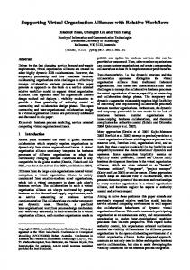
[email protected] For designers to remain in charge of their designs, they have to understand their circuits and the major relationships between the design variables and the circuit’s performances. Yet maintaining this insight is becoming increasingly difficult as problem complexity rises or when new technologies and devices are being utilized. Even when CAD tools are used, these need to be set up with the proper constraints in order to generate acceptable results. Setting up the constraints requires insight into the design problem and the circuit as well. Knowledge extraction tools are a means to accelerate designer insight. Enhanced insight leads to better decision-making in circuit sizing, behavioral modeling and verification, layout and topology design, regardless of the level of design automation. In this sense, knowledge extraction tools are a key way for CAD to build trust with designers, and are as such complementary to design automation tools. Symbolic analysis [1] and symbolic modeling [2][3] are examples of knowledge extraction tools. While symbolic analysis uses algorithmic methods to obtain analytic equations that characterize the circuit, symbolic modeling uses algorithms such as data mining to extract knowledge and design relations that might otherwise be “hidden” in raw data (e.g. simulation data). Because recent methods use SPICE simulation data as part of their inputs, they are general enough to cover arbitrary nonlinear circuits, technologies and analyses (e.g. transient) with good accuracy. Figure 1 illustrates this for the Caffeine tool [3] that uses genetic programming to evolve symbolic models that best fit the SPICE simulation data.
ABSTRACT The use of CMOS nanometer technologies at 65 nm and below will pose serious challenges on the design of mixed-signal integrated systems in the very near future. Rising design complexities, tightening time-to-market constraints, leakage power, increasing technology tolerances, and reducing supply voltages are key challenges that designers face. Novel types of devices, new process materials and new reliability issues are next on the horizon. We discuss new design methodologies and EDA tools that are being or need to be developed to address the problems of designing such mixed-signal integrated systems.
Categories and Subject Descriptors B.7.2 [Integrated Circuits]: Design aids –graphics, layout, placement and routing, simulation, verification
General Terms Algorithms, Design, Verification.
Keywords Analog, mixed-signal, integrated circuits, computer-aided design
1. Introduction Shrinking device geometries leads to two overarching trends: • More functionality is possible for the same area on a chip, which in nanometer-size geometries means systems on chips. • Device sizes get increasingly closer to the size of individual atoms, so variations become increasingly important. These trends correspond to two major challenges: handling system-level design, and handling process variations, both of which are an increase in problem complexity. We first discuss the problem of maintaining design insight in light of rising complexity and new processes. Then, we discuss tools and approaches that address system-level design and variation-aware design. Farther into the future, the same challenges will rise in difficulty; we discuss how structural synthesis might ultimately play a role and what other tools and methods will be needed.
2. Design Insight and Knowledge Extraction Permission to make digital or hard copies of all or part of this work for personal or classroom use is granted without fee provided that copies are not made or distributed for profit or commercial advantage and that copies bear this notice and the full citation on the first page. To copy otherwise, to republish, to post on servers or to redistribute to lists, requires prior specific permission and/or a fee. ICCAD'06, November 5-9, 2006, San Jose, CA Copyright 2006 ACM 1-59593-389-1/06/0011...$5.00
Figure 1: Knowledge extraction with CAFFEINE [3] that mines SPICE simulation data to produce template-free symbolic models.
461
the Filter, Comparator and DAC as part of its design space. The total runtime was about 3 days; in comparison the manual reference design took 6 months. Moreover, MOBU generated better designs; for example, one design had approximately the same performances but half the power consumption of the manual design [9].
3. System-Level Design Having a whole system on a chip leads to a whole host of challenges. But at the very core, the biggest challenge is the sheer complexity of the design. Doing the whole design “flat” is intractable, so hierarchical decomposition is necessary. So then, exactly how does one traverse the hierarchy? The top-down constraint driven methodology (TDCD) (e.g. [4]) is often assumed to be the “target methodology”, as in the MEDEA+ EDA roadmap [5]. But it has been tough to do in analog because of the issue of knowing what combinations of specifications are feasible. Two main alternatives have emerged in the literature: 1.
Doing bottom-up feasibility modeling as a precursor step to top-down constraint driven [6][7]
2.
Multi-objective bottom-up design (MOBU) [8][9][11].
4. Variation-Aware Design Designers not only have to deal with ever-larger designs, they also have to use ever-smaller devices. With that comes a continual increase in process variations, posing a threat to yield. The MEDEA+ roadmap [5] talks of yields of 95% at 0.35 μm, which reduce to just 50% at 90 nm. Variation-aware design needs good statistical modeling; unfortunately, such models have 9 to 15 or more random variables per device in the circuit [12]. As a result, the designer has to manage an unreasonable number of variables. The designer’s rules of thumb can disappear too; for example the common tactic of merely increasing area to reduce mismatch may actually not help much because of the nonlinear relation between W and L and mismatch in newer processes (Figure 6 in [12]).
Each has its own way of handling constraints and objectives. Both enable one to get an optimal system-level trade-off of possible combinations of specifications. Even after one has selected a hierarchical traversal approach, several issues remain, such as what method to use to estimate performances at all levels (e.g. using SPICE or behavioral simulators, regression-based models, etc.), how to handle interactions and mutual constraints between different subblocks, how to account for process variations, etc.
While Monte-Carlo sampling is a good first step to variationaware design, it doesn’t answer critical design questions such as identifying how design variables interact and affect yield. Caffeine [3] can address this: Figure 4 shows a Caffeinegenerated equation for Cpk (“process capability”) of a 50transistor amp having 68 design variables, which could subsequently be used for manual or automatic yield optimization.
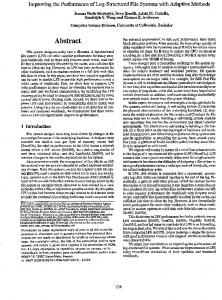
Figure 2: High–speed ǻȈ A/D modulator.
Figure 4: Amplifier, and an equation for its Cpk that was generated by the Caffeine tool [3]. rmsetest = 6.3%. As process scaling continues more flows and tools must be variation-aware. At first this may be by simply adding safety margins or post-design yield tuning; but ultimately all the design flows and tools will have to be statistically-centric from the start.
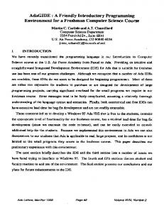
Figure 3: MOBU-style hierarchical traversal propagates trade-offs in a bottom-up fashion, maintaining all the sized designs along the way.
5. Topology Design
To give a flavor of the state of the art, MOBU was recently demonstrated in the design of a high–speed ǻȈ A/D modulator for a WLAN 802.11a/b/g standard [9]. The system-level topology is show in Figure 2. The hierarchical traversal proceeded as follows. The design was decomposed into seven separate subblocks, as shown in Figure 3. Then, at the very bottom block (GmC_Int), a multi-objective optimization was run, generating a set of designs, each trading off some specs for others [10]. At the Filter block, there were three integrators, each of which could be any of the designs created in the GmC_Int optimization. Three multiobjective optimizations generated trade-offs for the Filter, Comparator, and DAC respectively. Finally, a multi-objective optimization was run at the ADC level, using the trade-offs from
Moore’s Law will continue to march on, so big systems will get even bigger and process variations will have even more variation. Gates will be leakier, and materials will continue to change. In addition, supply voltages will be scaling, reducing the headroom for analog circuits. All this has implications for circuit topology design, since existing topologies may not function anymore. Also, gates are becoming virtually free, giving opportunities to use digital logic to construct or calibrate analog behavior. This all leads to challenges (opportunities) for topology design, manual and automatic. Two approaches for automated topology generation can be distinguished: Approach 1. In the “building-block substitution” approach, an optimal topology is found by iteratively substituting different
462
subblock implementations in some predefined topology template. This could be done manually where the designer goes from abstract specification down to detailed design, or could be driven by the specification in an optimization loop like in Darwin [13]. An example of recent results in ADC design [14] is in Figure 5 (left), which shows example operators that drill down towards implementation. By putting those sorts of operators into a multiobjective optimization framework, a whole set of trustworthy topologies can be generated, as Figure 5 (right) illustrates. Approach 2. Structural synthesis that generates truly novel designs, driven by the specifications. At the cell level, the closest we have seen is [15], which used genetic programming to automatically reinvent some small circuits from around-2000 patents, a pretty impressive feat. Unfortunately, the computational resources needed to generate those were incredibly high, and if the circuit problems were modeled with more industrial constraints, then the runtime would be about 150 years on a 1000node 1-GHz cluster [16].
ACKNOWLEDGEMENTS Funding for the reported research results is acknowledged from IWT/Medea+ Uppermost, Solido Design Automation and FWO Flanders.
REFERENCES [1]
[2]
[3]
[4]
[5] [6] [7]
Figure 5: Left: Example “topology refinement” operators. Right: System-level performance trade-offs; the tool automatically selects the most promising topology for each combination of specifications.
[8]
[9]
In our opinion, trust is an even bigger issue than computational cost. Trust issues occur whenever previously-unseen substructures are generated by the synthesis tool. For designers to really trust a novel circuit, they need to see it working in silicon. Structural circuit synthesis can be helpful to accelerate development of new design techniques in new processes, new devices, etc. …. for automated or manual flows. This use case has actually been happening in other domains such as quantum circuit design [17] and multi-valued logic design [18].
[10]
[11]
[12]
The MEDEA+ roadmap targets “analog [structural] synthesis” for 2009-2010. AMS CAD will certainly notch up a level of excitement when this dream becomes reality.
[13] [14]
6. Conclusions
[15] [16]
Moore’s Law will keep charging, leading to increased complexities at the very top (system-level design) and at the very bottom (variations gone crazy). We have discussed CAD research that addresses hierarchical system-level design and variationaware design. We have emphasized the importance for the designer to maintain insight into the circuit and how tools can help in knowledge extraction. Going farther into the future, we expect a need for more tools in signal integrity analysis (such as EMC analysis), for more automated model generation, for more accurate modeling at higher operating frequencies and for true structural synthesis at both circuit and system levels.
[17]
[18]
463
G. Gielen, “Techniques and Applications of Symbolic Analysis for Analog Integrated Circuits: A Tutorial Overview”, in Computer Aided Design of Analog Integrated Circuits And Systems, R.A. Rutenbar et al., eds., IEEE, pp. 245-261, 2002. W. Daems, et al. "Simulation-based generation of posynomial performance models for the sizing of analog integrated circuits," IEEE Trans. CAD 22(5), May 2003, pp. 517-534. T. McConaghy, et al., “CAFFEINE: Template-Free Symbolic Model Generation of Analog Circuits via Canonical Form Functions and Genetic Programming”, Proc. DATE 2005. H. Chang, et al. A Top–Down, Constraint–Driven Design Methodology for Analog Integrated Circuits. Kluwer Academic Publishers, 1997. MEDEA+ EDA Roadmap, Version 5, 2005, http:///www.medeaplus.org F. De Bernardinis, et al, “Support Vector Machines for Analog Circuit Performance Representation,” Proc. DAC 05 D. Mueller, et al. “Deterministic Approaches to Analog Performance Space Exploration”, Proc. DAC 2005, pp. 869874, 2005. T. Eeckelaert, et al. “Efficient Multiobjective Synthesis of Analog Circuits using Hierarchical Pareto–optimal Performance Hypersurfaces,” Proc. DATE, 2005. T. Eeckelaert, et al. “Hierarchical Bottom-up Analog Optimization Methodology Validated by a Delta-Sigma A/D Converter Design for the 802.11 a/b/g Standard,” Proc. DAC, pp. 25-30, 2006. B. De Smedt, G. Gielen, “WATSON: Design Space Boundary Exploration and Model Generation for Analog and RF IC Design,” IEEE TCAD 22(2), Feb. 2003, pp. 213–224. S. Tiwary, P. Tiwary, R. Rutenbar, “Generation of YieldAware Pareto Surfaces for Hierarchical Circuit Design Space Exploration,” Proc. DAC 2006, pp. 31-56, 2006. P. Drennan et al. “Understanding MOSFET Mismatch for Analog Design,” IEEE JSSC, Vol. 38, pp.450-456, 2003. W. Kruiskamp, et al., “DARWIN: CMOS Opamp Synthesis by means of a Genetic Algorithm”, Proc. DAC, 1995. E. Martens, G. Gielen, “Top-Down Heterogenous Synthesis of Analog and Mixed-Signal Systems,” Proc. DATE, 2006. J.R. Koza, et al., Genetic Programming IV, Kluwer, 2003. T. McConaghy, G. Gielen, “Genetic Programming in Industrial Analog CAD: Applications and Challenges”, Genetic Programming Theory and Practice III, ch. 19, pp. 291-306, 2005. L. Spector, H. Bernstein, “Communication Capacities of Some Quantum Gates, Discovered in Part through Genetic Programming,” In Proc. Intl. Conf. on Quantum Comm., Measurement., and Computing, pp. 500-503, 2003. J. Miller, et al., “The Genetic Algorithm as a Discovery Engine: Strange Circuits and New Principles,” in Proc. AISB Symp. on Creative Evolutionary Systems, UK, 1999.