as record efficiency silicon solar cells at the same bandgap, indicating the ..... range, confirming that it is a good assumption that Voc and. Eg are related by an ...
International Conference on Solar Concentrators for the Generation of Electricity or Hydrogen, 1-5 May 2005, Scottsdale, Arizona (NREL/CD-520-38172)
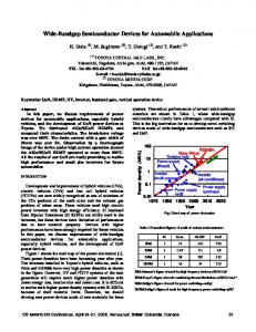
Bandgap Engineering in High-Efficiency Multijunction Concentrator Cells R. R. King, R. A. Sherif, G. S. Kinsey, S. Kurtz1, C. M. Fetzer, K. M. Edmondson, D. C. Law, H. L. Cotal, D. D. Krut, J. H. Ermer, and N. H. Karam Spectrolab, Inc., Sylmar, CA 1 National Renewable Energy Laboratory, Golden, CO
1.
Introduction Multijunction concentrator solar cells[1-3] for terrestrial applications have reached the point at which the next set of technology improvements are likely to push efficiencies over 40%. Very high solar cell efficiencies are crucial to the cost-effective commercialization of concentrator and flat-plate photovoltaic systems alike[4-8], because of the highly leveraging effect that efficiency has on module packaging and balance-of-system costs. This paper discusses the semiconductor device research paths being investigated with the aim of reaching the 40% efficiency milestone and higher. A central theme for many of these research thrusts is to change the partition of the solar spectrum afforded by the subcell bandgaps in multijunction cells, to one more advantageous for efficient energy conversion. To this end, lattice-mismatched, or metamorphic, subcell materials, unconventional alloys such as GaInNAs, and cell structures with more than 3 junctions are being investigated with the goal of exceeding 40% solar cell efficiencies.
Motivation – PV Concentrator Economics An important question that motivates much of the strategy in photovoltaic research is "Why hasn't photovoltaic electricity generation become widespread to date?" A widely-referenced and very useful cost study by Swanson that helps to answer this question can be found in [8]. In that paper, a wide variety of flat-plate and concentrator PV technologies are evaluated for their economic effectiveness. We adapted the methodology in [8] for a slightly different purpose, to find the dependence of the cost effectiveness of a photovoltaic system on the cell cost per unit area, in order to determine the suitable range of cell cost. Using a simple expression given in Fig. 1, the PV system cost per kWhr over a 5 year payback period was calculated as a function of cell cost per unit area, taking into account: typical module packaging, tracking, balance-of-system (BOS), and similar costs documented in [8]; module optical efficiency and cost differences for flat-plate and concentrator systems; the ability to use the global and direct solar resource for flatplate and concentrator systems; in addition to the variable cell cost. The resulting curves of the average cost of electricity in $/kWhr generated by the system in 5 years, plotted in Fig. 1, show that both flat-plate and concentrator systems can reach electricity costs below a near-term target value of 0.15 $/kWhr for at least some combinations of high efficiency and low cell cost.
0.3
500X Point-Focus Conc.
Fixed Flat-Plate
3.3
Cell cost ranges
0.2
2.2
10% 20%
5-Year Payback Threshold, at $0.15/kWh 15%
0.1
30%
20%
0.0 0.001
1.1
40%
25% cell eff.
50% cell eff.
module tracking BOS, area BOS, power peak power cell + + + + PV system cost 2 2 cost / m 2 cost / m 2 cos t / m 2 cos t / W output, W/m cost / m per kWh generated in = 5 year energy produced, 5 year payback period kWh m 2 ⋅ year payback period
(
0.01
0.1
conc. ratio
)
2
1
PV System Cost / Power Output ($/W)
This paper discusses semiconductor device research paths under investigation with the aim of reaching the milestone efficiency of 40%. A cost analysis shows that achieving very high cell efficiencies is crucial for the realization of cost-effective photovoltaics, because of the strongly leveraging effect of efficiency on module packaging and balance-of systems costs. Latticematched (LM) GaInP/ GaInAs/ Ge 3-junction cells have achieved the highest independently confirmed efficiency at 175 suns, 25°C, of 37.3% under the standard AM1.5D, low-AOD terrestrial spectrum. Latticemismatched, or metamorphic (MM), materials offer still higher potential efficiencies, if the crystal quality can be maintained. Theoretical efficiencies well over 50% are possible for a MM GaInP/ 1.17-eV GaInAs/ Ge 3junction cell limited by radiative recombination at 500 suns. The bandgap – open circuit voltage offset, (Eg/q) – Voc, is used as a valuable theoretical and experimental tool to characterize multijunction cells with subcell bandgaps ranging from 0.7 to 2.1 eV. Experimental results are presented for prototype 6-junction cells employing an active ~1.1-eV dilute nitride GaInNAs subcell, with active-area efficiency greater than 23% and over 5.3 V open-circuit voltage under the 1-sun AM0 space spectrum. Such cell designs have theoretical efficiencies under the terrestrial spectrum at 500 suns concentration exceeding 55% efficiency, even for latticematched designs.
2.
PV System Cost / kWh Generated in 5 Year Period ($/kWh)
ABSTRACT
0.0 10
Cell Cost ($/cm ) Cell cost ranges, module and BOS costs from: Swanson, Prog. Photovolt. Res. Appl. 8, 93-111 (2000).
Figure 1. Average cost of electricity produced over a 5 year payback period, in $/kWhr, as a function of cell cost per unit area. Two distinct domains can be seen: flat-plate systems which require very low cell cost to be cost effective, and concentrator systems which can tolerate high cell cost.
Two families of curves are evident in Fig. 1: those for flat-plate systems for which very low cell costs are required, and those for concentrators for which relatively high cell costs can be tolerated. Note that below about 12% efficiency for flat-plate, and about 20% efficiency for concentrator systems, a PV system cannot become cost effective in 5 years even for zero cell cost, due to the cost of module packaging, BOS, and similar costs. Cost effective flat-plate systems need to be in the range of 0.1-1.0 cents per cm2 cell cost for 20%-efficient cells, while for concentrator systems with 30%-efficient cells, a cell cost of 1-5 dollars per cm2 , or 500-1000× greater, is suitable for cost effectiveness. Both efficiency values are reasonable for the two technologies, but using the typical cell cost ranges cited in [8], indicated in Fig. 1, it can be seen that the challenge for flat-plate technologies is to reduce present typical cell costs of 0.02-0.04 $/cm2 by an order of magnitude, maintaining cell efficiencies of 20%, while for concentrator systems 30% cells are cost effective now, and the challenge is to reach higher efficiencies in the 40-50% range for greater cost effectiveness. A large part of the answer to the question posed at the beginning of the section is that solar energy is a dilute resource, and low-efficiency systems require very large areas of glass, metal, and plastic needed for module packaging, support structures, wiring, etc. Even without considering the cost of semiconductor materials, the costs of those relatively mundane materials over large areas can preclude cost effectiveness. Fortunately, highefficiency solar cells strongly reduce the module area needed for a given electric power output, and strongly leverage module and BOS costs, and with the use of ~500× concentration, relatively high cell costs per area can be tolerated. Taking cell efficiencies into the 4050% range may well be the clearest path to photovoltaic cost effectiveness. 3.
Cell Designs and Theoretical Efficiency
Multijunction Cell Architectures The division of the solar spectrum by the 1.8 eV/ 1.4 eV/ 0.67 eV combination of bandgaps in a latticematched (LM) GaInP/ GaInAs/ Ge 3-junction cell leads to excess photogenerated current density in the Ge subcell. Part of this wasted current can be used effectively in the middle cell if its bandgap is lowered, as in lattice-mismatched, or metamorphic (MM) GaInP/ GaInAs/ Ge 3-junction cells with a 1.2-1.3 eV GaInAs middle cell [1, 9-15]. The challenge then becomes to maintain low Shockley-Read-Hall (SRH) recombination due to defects in these mismatched materials. Higher lattice mismatches give still greater advantages if the crystal quality can be maintained. Studies of highly-lattice-mismatched single-junction GaInAs cells were conducted with indium compositions ranging from 0% to 35% indium content in 0.95-eV Ga0.65In0.35As cells with 2.4% lattice mismatch to the Ge substrate[1].
Minority-carrier properties of these mismatched GaInAs materials and GaInP at the same lattice constant were explored. At a bandgap of 1.1 eV, GaInAs cells with 1.6% lattice mismatch have nearly the same open-circuit voltage as record efficiency silicon solar cells at the same bandgap, indicating the degree to which defects have been suppressed by optimization of the step-graded buffers in these metamorphic devices. The dislocation density in these Ga0.77In0.23As materials is 3-4 × 106 cm-2, as measured by plan-view TEM and cathodoluminescence[1]. TEM imaging over a large sample area indicates a dislocation density of only 2 × 106 cm-2 for Ga0.65In0.35As with ~0.95-eV bandgap, consistent with the observation that the minority-carrier lifetime measured by time-resolved photoluminescence (TRPL) is about 10 ns for both the 1.1- and 0.95-eV materials[1]. These metamorphic materials enable advanced multijunction cell designs incorporating a 0.9-1.1 eV subcell. Work in this area has yielded cell results on metamorphic Ga0.44In0.56P/ Ga0.92In0.08As/ Ge 3-junction cells, with the upper two cells having a lattice constant 0.5% larger than the Ge substrate [1,9]; Ga0.35In0.65P/ Ga0.83In0.17As cells [7]; 2- and 3-junction Ga0.29In0.71P/ Ga0.77In0.23As/ Ge cells [14,15]; and on GaInP/ GaAs/ 1-eV GaInAs 3-junction cells with the upper two subcells lattice matched to a GaAs substrate [16,17]. Schematics of this latter cell design are shown in Fig. 2. Another way to utilize the excess photogenerated current in the Ge subcell in 3-junction cells is to insert a ~1-eV semiconductor, such as GaInNAs lattice-matched to Ge, above the Ge subcell. 5- and 6-junction cell designs partition the solar spectrum into narrower wavelength ranges than 3-junction cells, allowing all the subcells to be current matched to the low-current-producing GaInNAs subcell. Additionally, the finer division of the incident spectrum reduces thermalization losses from electron-hole pairs photogenerated by photons with energy far above the bandgap energy, and the smaller current density in 5- and 6junction cells lowers resistive I2R losses. Cross-sectional diagrams of 5- and 6-junction cells are drawn in Fig. 3.
AR
metal cap
AR
1.9 eV (Al)GaInP subcell 1 1.424 eV GaAs subcell 2
GaAs substrate
GaAs or Ge substrate cap
graded MM buffer layers 1.0 eV GaInAs subcell 3
1.9 eV (Al)GaInP subcell 1 1.424 eV GaAs subcell 2 graded MM buffer layers 1.0 eV GaInAs subcell 3
(a)
(b)
Figure 2. Two configurations of 3-junction solar cells with a highly-lattice-mismatched, inverted 1-eV GaInAs bottom subcell: (a) growth on two sides of a transparent GaAs substrate; (b) growth on the back of a GaAs or Ge substrate that is removed during cell fabrication.
1.17 eV, the optimum subcell 3 becomes 0.69 eV, coinciding very closely with the bandgap of Ge, with a calculated efficiency of over 55%.
contact AR
AR cap contact AR
AR cap
(Al)GaInP Cell 1
(Al)GaInP Cell 1
2.0 eV
wide-Eg tunnel junction
2.0 eV
wide-Eg tunnel junction
GaInP Cell 2 (low Eg) 1.8 eV wide-Eg tunnel junction
wide-Eg tunnel junction
wide-Eg tunnel junction
Ga(In)As Cell 3 1.41 eV
Ga(In)As Cell 4 1.41 eV
tunnel junction
tunnel junction
GaInNAs Cell 4 1.1 eV
GaInNAs Cell 5 1.1 eV
tunnel junction
tunnel junction
Ga(In)As buffer
Ga(In)As buffer
nucleation
nucleation
Ge Cell 5 and substrate 0.67 eV back contact
Ge Cell 6 and substrate 0.67 eV back contact
Figure 3. Cross-sections of 5- and 6-junction cells. At a given lattice mismatch, higher efficiencies can be reached in many multijunction cell designs if the GaInP top cell bandgap is increased, since less light then needs to be leaked through the GaInP to the GaInAs cell beneath, and more can be converted at the higher voltage of the GaInP top cell. The effect of disordering Ga and In atoms on the group-III sublattice, is known to increase the bandgap by ~100 meV for the LM case. This effect has been confirmed to persist in lattice-mismatched, Inrich compositions of GaInP as well[11,14]. Use of AlGaInP to raise the top cell bandgap can also increase the multijunction cell efficiency[2,11]. Theoretical efficiency The theoretical efficiency of multijunction solar cells limited by the fundamental mechanism of radiative recombination was calculated as a function of subcell bandgap in 3- and 6-junction cells, at 25°C. The current density in each subcell was found from the photon flux in each photon energy range of the standard terrestrial AM1.5D, low-AOD spectrum[18], the open-circuit voltage from the carrier concentration at which radiative recombination is in steady state with this photogenerated current density, and the cell efficiency was found by combining the current-voltage characteristics of the subcells in the multijunction stack. The calculated efficiencies for 3-junction cells are plotted in Fig. 4. The familiar case of a GaInP/ GaInAs/ Ge 3-junction solar cell can be found in the right-hand set of curves. For the lattice-matched case with a 1.41eV GaInAs subcell 2, the optimum top cell bandgap is about 1.9 eV. As one goes to lower bandgaps for subcell 2, as for MM GaInAs, the optimum top subcell Eg shifts down as well, reaching ~1.74 eV at the optimum subcell 2 bandgap of 1.17 eV, for a calculated efficiency over 55%. For a 1.4-eV subcell 2, a higher efficiency can be achieved with a 1.0-eV bottom subcell than for a Ge subcell, as can be seen in the left-hand set of curves in Fig. 4. The theoretical efficiency for this case with a 1.0-eV subcell 3, corresponding to the cell configurations sketched in Fig. 2, is ~53%. Interestingly, as the middle subcell 2 bandgap drops to
1.41 eV GaInAs subcell 2 1.3 eV 1.17 eV 1.14 eV 1.10 eV 1.05 eV
56% 3-Junction Cell Theoretical Efficiency (%)
AlGa(In)As Cell 3 1.6 eV
54%
500 suns AM1.5D, low-AOD
52%
50%
GaInAs subcell 3 (optimized Eg for subcell 1)
48%
AlGaInP subcell 1 (0.67 eV Eg for Ge subcell 3)
46%
44% 0.4
0.6
0.8 1.0 1.2 1.4 1.6 1.8 AlGaInP Subcell 1 Bandgap or GaInAs Subcell 3 Bandgap (eV)
2.0
Figure 4. Theoretical efficiency of 3-junction solar cells limited only by radiative recombination, as a function of the bandgap of the (top) subcell 1 material such as AlGaInP, and the (bottom) subcell 3 material, such as Ge, GaInNAs, or lattice-mismatched GaInAs.
1.9 eV AlGaInP subcell 1 2.1 eV 2.3 eV 2.35 eV 1.00 eV GaInNAs subcell 5 1.1 eV 1.18 eV 1.22 eV
58% 6-Junction Cell Theoretical Efficiency (%)
AlGa(In)As Cell 2 1.7 eV
56%
54%
500 suns AM1.5D, low-AOD
52%
50% varying GaInNAs subcell 5
48%
varying AlGaInP subcell 1
46% 0.7
0.9
1.1
1.3
1.5
1.7
1.9
2.1
2.3
2.5
AlGaInP Subcell 1 Bandgap or GaInNAs Subcell 5 Bandgap (eV)
Figure 5: Theoretical efficiency of 6-junction solar cells limited only by radiative recombination, as a function of the bandgap of the (top) subcell 1 material such as AlGaInP, and the subcell 5 material on top of the Ge subcell 6, such as GaInNAs, or lattice-mismatched GaInAs. Figure 5 plots the theoretical efficiency of 6-junction cells under the concentrated terrestrial spectrum, again at 25°C. The bandgaps of subcells 2, 4, and 6 were assumed to be 1.8 eV corresponding to ordered GaInP, 1.41 eV for LM 1%-In GaInAs, and 0.67 for the Ge substrate, respectively. Higher efficiencies are possible for full flexibility in bandgap. For optimum top subcell Eg of 2.3 eV and subcell 5 Eg of 1.18 eV, efficiencies over 56% are possible for a lattice-matched configuration using GaInNAs for subcell 5, or for metamorphic configurations using MM 1.18-eV GaInAs in subcell 5. Subcell 1 bandgaps of 1.9 or 2.1 eV, which are easier to achieve, still yield theoretical efficiencies of 53.2% and 54.7%, respectively.
4.
−Eg / kT
ni2 = NC NV e
Results and Discussion
0.96 eV
1.08
1.30 1.26
1.40 1.38
Metamorphic semiconductor materials Internal quantum efficiency (QE) data of metamorphic GaInAs solar cells grown on Ge substrates, with bandgaps ranging from 1.4 to 0.96 eV, are plotted in Fig. 6, showing the progression of the absorption edge with increasing lattice mismatch. Note that the near-bandedge QE remains very high out to 1.08-eV GaInAs, falling only moderately at 0.96 eV, indicating long minoritycarrier diffusion lengths given the large latticemismatches of 1.6% for 1.08-eV and 2.4% for 0.96-eV GaInAs. These long diffusion lengths result from the long minority-carrier lifetimes measured in these materials[1], and translate into the high open-circuit voltages discussed above.
Internal Quantum Efficiency (%)
100 90 80 70 60
GaInAs single-junction solar cells
50 40 30 20 10 0 300
400
500
600
700 800 900 1000 1100 1200 1300 1400 Wavelength (nm)
Figure 6. Measured internal QE curves for singlejunction GaInAs cells, showing the shift in wavelength corresponding to the bandgap, and strong response near the bandgap wavelength indicating long diffusion lengths in these metamorphic materials. Bandgap-voltage offset When investigating semiconductors with a wide range of bandgaps for use in solar cells, a method to gauge the material quality is needed, that can compare non-ideal recombination properties in one material to those in another. The difference between the bandgap voltage Vg = Eg /q and open-circuit voltage Voc, is a useful quick gauge of semiconductor quality for many different materials systems[11]. The smaller this offset voltage (Eg/q) - Voc , the closer the electron and hole quasi-Fermi levels are to the conduction and valence band edges, respectively, and the more closely the voltage approaches the fundamental limit set by radiative recombination. This observation is based on the dependence of open-circuit voltage on bandgap in a solar cell in which the only recombination mechanism is radiative:
Voc =
kT J ph ln q qwB ni2
(1)
Voc =
Eg q
−
kT qwBNC NV ln q J ph
(2)
(3)
where Jph is the photogenerated current density, w is the thickness of the solar cell base, ni is the intrinsic carrier concentration, B is the radiative recombination coefficient, and the other symbols have their usual meaning. Note that the logarithmic second term in Eqn. 3 depends only weakly on Eg , resulting in a nearly constant offset voltage (Eg /q) Voc between the bandgap and the calculated Voc for solar cells limited by radiative recombination, across a wide range of bandgaps. Thus the difference between the measured open-circuit voltage and the Voc predicted in the radiative limit can be used to determine the non-radiative recombination components, primarily Shockley-Read-Hall (SRH) recombination. When typical values for NC, NV, B, w, Jph, and their dependences on bandgap are plugged into Eqn. 1, the difference (Eg /q)-Voc varies only from ~0.31 V to 0.39 V in the radiative limit, for bandgaps ranging from 0.95 to 2.0 eV. One way to visualize the approximate constancy of (Eg/q) - Voc for different semiconductors is that B varies only slowly with Eg , and therefore the pn product in steady state, in which the photogenerated current per unit volume Jph/qw equals the radiative recombination rate Bnp, is roughly similar for a given incident photon flux. Because the density of states in the conduction band is similar for many semiconductors, and the same is true for the valence band, similar p and n among different semiconductors in steady state translates to roughly the same energy difference between the conduction band edge and the electron quasiFermi level, and the same is true between the valence band edge and the hole quasi-Fermi level. Since the cell voltage is the difference between electron and hole quasi-Fermi levels, and these quasi-Fermi levels have a constant offset from their respective band edges, the cell voltage differs from the bandgap voltage by a constant value, to first order. Fig. 7 plots the measured open-circuit voltage for singlejunction cells with a wide range of bandgaps, from 0.67 to 2.1 eV, against the bandgaps of the solar cell bases from quantum efficiency measurements of the absorption edge. Also plotted is the experimental bandgap-voltage offset, (Eg/q) - Voc , and the ideal bandgap-voltage offset limited by radiative recombination. The experimental Voc values closely parallel the measured Eg over the broad bandgap range, confirming that it is a good assumption that Voc and Eg are related by an additive constant. At the 1.4-eV bandgap of 1%-In GaInAs, the experimental bandgapvoltage offset is nearly equal to that calculated in the radiative limit at about 370 mV, indicating that almost all of the recombination in this lattice-matched material is radiative, and only a small component is SRH recombination. Materials with higher lattice mismatch, such as 1.1-eV and 0.97-eV GaInAs have offset voltages in the 430-490 mV range, remarkably low in light of the 1.6% and 2.4% lattice mismatches of these materials, respectively.
1.8
Figure 7. Experimental Voc for a wide range of singlejunction solar cell bandgaps, from 0.67 to 2.1 eV, showing that the bandgap-voltage offset, (Eg /q) - Voc , is roughly constant over this range as predicted from theory. The value of this offset approaches the radiative limit for some solar cell materials. 3-junction cell results Lattice-matched GaInP/ GaInAs/ Ge 3-junction cells have achieved the highest independently confirmed efficiency of 37.3% at 175 suns[1,19] under the AM1.5D, low-AOD spectrum, the standard reporting spectrum used by the National Renewable Energy Laboratory[18]. Metamorphic GaInP/ GaInAs/ Ge 3junction devices, with 8%-In in the middle cell base, at a 0.5% lattice mismatch with respect to the Ge substrate, have achieved 36.9% efficiency under the same AM1.5D, low-AOD spectrum at NREL, reaching parity with the lattice-matched case in spite of the threading dislocations that can result from lattice mismatch[1]. 6-junction cell results Prototype 6-junction AlGaInP/ GaInP/ AlGaInAs/ GaInAs/ GaInNAs/ Ge cells with an active ~1.1-eV GaInNAs subcell 5 have been built and tested. Measured quantum efficiencies of all six of the individual subcells for the 6-junction (6J) cell grown separately are plotted in Fig. 8. The bandgaps of each subcell can be noted from the photon energy axis. The top subcell 1 is intentionally grown thin and transparent to light over much of its response range, in order to current match to the other subcells. The QE of the GaInNAs subcell 5, remains the most challenging. This cell is highly sensitive to annealing, including the thermal budget that the nitride cell experiences when the upper four subcells of the 6-junction cell are grown on top of it. This sensitivity is depicted in the GaInNAs cell QE measurements in Fig. 9. With a suitably low thermal budget, 8.5 mA/cm2 current density can be achieved under the AM0 space spectrum, enough to current match the nitride cell to the other 6J subcells. The measured I-V characteristics of fully-integrated 6junction cells are shown in Fig. 10. Open-circuit voltage of 5.33 V, and preliminary efficiencies of 23.6% activearea, and 20.9% total area were measured, representing a
2.2
60 50
60
40 30
40
20 20
Curr. Dens. Per Unit Photon 2. Energy (mA/(cm eV))
1.4 Bandgap Eg (eV)
70
10 0
0 0.5
1.0
1.5
2.0
2.5
3.0
3.5
Photon Energy (eV)
Figure 8. Quantum efficiency measurements of the six component subcells of a 6-junction solar cell, plotted vs. photon energy. 100
GaInNAs subcell 5: Effect of upper subcell growth for 5 & 6J cells
90 80
Low thermal budget Jsc = 8.5 mA/cm2
70 60
Eg = 1.05 eV
1
Quantum Efficiency (%)
0.6
80
Ext. Quantum Efficiency (AR-coated) (%)
0.0
50 40 30 20 High thermal budget Jsc = 5.1 mA/cm2
10 0 800
900
1000
1100
1200
1300
Wavelength (nm)
Figure 9. Measured quantum efficiency of 1.05-eV GaInNAs solar cells near the Ge lattice constant, showing the effect of thermal budget. 6-junction AlGaInP/ GaInP/ AlGaInAs/ GaInAs/ GaInNAs/ Ge solar cells
8 7
Current Density (mA/cm2)
d-AlGaInP
d-AlGaInP
d-AlGaInP
d-GaInP
AlGaInAs
o-GaInP
AlGaInAs
1.4-eV GaInAs GaAs
1.30-eV GaInAs
GaInNAs
1.24-eV GaInAs
0.5
1.91-eV GaInP Cell 1 EQE 1.81-eV GaInP Cell 2 EQE 1.57-eV AlGaInAs Cell 3 EQE 1.39-eV GaInAs Cell 4 EQE 1.05-eV GaInNAs Cell 5 EQE 0.67-eV Ge Cell 6 EQE 6J, cumulative EQE AM0
100
1.10-eV GaInAs
1.0
0.97-eV GaInAs
Voc Eg from EQE (Eg/q) - Voc radiative limit
1.5
Ge (indirect gap)
Eg/q, Voc, and (Eg/q) - Voc (V)
substantial increase over the 5.11 V and 13.47% efficiency for the first 6-junction cells tested [1]. These improvements bode well for the development of MJ cells with more than 3 junctions to increase the efficiency of terrestrial concentrator cells.
Voc of solar cells with wide range of bandgaps and comparison to radiative limit
2.0
6
Anneal condition 1 5
Anneal condition 2
4
Anneal condition 3 Voc = 5.334 V
3
Jsc = 7.30 mA/cm2 (active area) FF = 82.0% prelim. active area eff. = 23.6% prelim. total area eff. = 20.9% AM0, 0.1353 W/cm2, 28oC, 0.26 cm2
2 1 0 0
1
2
3
Voltage (V)
4
5
6
Figure 10: Illuminated current-voltage characteristics for 6junction AlGaInP/ GaInP/ AlGaInAs/ GaInAs/ GaInNAs/ Ge solar cells, with an active ~1.1-eV GaInNAs subcell 5, with Voc over 5.3V.
5.
Summary
The device elements for a variety of solar cell architectures capable of reaching 40% efficiency have been demonstrated. These include the use of metamorphic materials for greater freedom of bandgap selection, wider-bandgap top cell materials such as AlGaInP and alloys with a disordered group-III sublattice, and cell architectures with 3 to 6 junctions that make use of the excess current density in the Ge subcell of conventional 3-junction cells. By combining these device structure advances under investigation in research groups around the world, the goal of a practical 40%-efficient photovoltaic cell is near. 5.
Acknowledgments
The authors would like to thank Martha SymkoDavies, Bob McConnell, Keith Emery, James Kiehl, Tom Moriarty, Wyatt Metzger, Richard Ahrenkiel, Brian Keyes, Manuel Romero, Dan Friedman, and Jerry Olson at NREL; and Peter Colter, Takahiro Isshiki, Moran Haddad, Kent Barbour, Mark Takahashi, and Greg Glenn, and the entire multijunction solar cell team at Spectrolab. This work was supported in part by the Dept. of Energy through the NREL High-Performance PV program (NAT-1-30620-01), by the Air Force Research Laboratory (AFRL/VS) under DUS&T contract # F29601-98-2-0207, and by Spectrolab. 6.
References
[1] R. R. King, C. M. Fetzer, K. M. Edmondson, D. C. Law, P. C. Colter, H. L. Cotal, R. A. Sherif, H. Yoon, T. Isshiki, D. D. Krut, G. S. Kinsey, J. H. Ermer, Sarah Kurtz, T. Moriarty, J. Kiehl, K. Emery, W. K. Metzger, R. K. Ahrenkiel, and N. H. Karam, "Metamorphic III-V Materials, Sublattice Disorder and Multijunction Solar Cell Approaches with Over 37% Efficiency," Proc. 19th European Photovoltaic Solar Energy Conf., Paris, France, 7-11 June 2004, p.3587. [2] T. Takamoto, T. Agui, K. Kamimura, M. Kaneiwa, M. Imaizumi, S. Matsuda, and M. Yamaguchi, "Multijunction Solar Cell Technologies – High Efficiency, Radiation Resistance, and Concentrator Applications," Proc. 3rd World Conf. on Photovoltaic Energy Conversion, Osaka, Japan, May 11-18, 2003, p. 581. [3] A. W. Bett, F. Dimroth, M. Hein, G. Lange, M. Meusel, U. Schubert, G. Siefer, "Development of III-V-Based Concentrator Solar Cells and Their Application in PV Modules," Proc. 29th IEEE Photovoltaic Specialists Conf., New Orleans, Louisiana, May 19-24, 2002, p. 844. [4] R. A. Sherif, R. R. King, N. H. Karam, and D. R. Lillington, "The Path to 1 GW of Concentrator Photovoltaics Using Multijunction Solar Cells," Proc. 31st IEEE Photovoltaic Specialists Conf., Lake Buena Vista, Florida, Jan. 3-7, 2005, p. 17. [5] R.A. Sherif, H.L. Cotal, R.R. King, A. Paredes, N.H. Karam, G.S. Glenn, D. Krut, A. Lewandowski, C. Bingham, K. Emery, M. Symko-Davies, J. Kiehl, S. Kusek, and H. Hayden, "The Performance and Robustness of GaInP/InGaAs/Ge Concentrator Solar Cells in High Concentration Terrestrial Modules," Proc. 19th European Photovoltaic Solar Energy Conf., Paris, France, 7-11 June 2004, p. 2074. [6] K. Araki, M. Kondo, H. Uozumi, M. Yamaguchi, "Development of a Robust and High-Efficiency Concentrator Receiver," Proc. 3rd World Conf. on Photovoltaic Energy Conversion, Osaka, Japan, May 11-18, 2003, p. 630.
[7] A. Bett, C. Baur, F. Dimroth, G. Lange, M. Meusel, S. van Riesen, G. Siefer, V. M. Andreev, V. D. Rumyantsev, N. A. Sadchikov, "FLATCONTM-Modules: Technology and Characterisation," Proc. 3rd World Conf. on Photovoltaic Energy Conversion, Osaka, Japan, May 1118, 2003, p. 634. [8] R. M. Swanson, "The Promise of Concentrators," Progress in Photovoltaics: Res. Appl. 8, pp. 93-111 (2000). [9] R. R. King, M. Haddad, T. Isshiki, P. C. Colter, J. H. Ermer, H. Yoon, D. E. Joslin, and N. H. Karam, "Metamorphic GaInP/GaInAs/Ge Solar Cells," Proc. 28th IEEE Photovoltaic Specialists Conf., Anchorage, Alaska, Sep. 15-22, 2000, p. 982. [10] F. Dimroth, U. Schubert, and A. W. Bett, "25.5% Efficient Ga0.35In0.65P/Ga0.83In0.17As Tandem Solar Cells Grown on GaAs Substrates," IEEE Electron Device Lett., 21, p. 209 (2000). [11] R. R. King, C. M. Fetzer, P. C. Colter, K. M. Edmondson, J. H. Ermer, H. L. Cotal, H. Yoon, A. P. Stavrides, G. Kinsey, D. D. Krut, N. H. Karam, "High-Efficiency Space and Terrestrial Multijunction Solar Cells Through Bandgap Control in Cell Structures," Proc. 29th IEEE Photovoltaic Specialists Conf., New Orleans, Louisiana, May 19-24, 2002, p. 776. [12] R. R. King, C. M. Fetzer, P. C. Colter, K. M. Edmondson, D. C. Law, A. P. Stavrides, H. Yoon, G. S. Kinsey, H. L. Cotal, J. H. Ermer, R. A. Sherif, K. Emery, W. Metzger, R. K. Ahrenkiel, and N. H. Karam, "LatticeMatched and Metamorphic GaInP/GaInAs/Ge Concentrator Solar Cells," Proc. 3rd World Conf. on Photovoltaic Energy Conversion, Osaka, Japan, May 11-18, 2003, p. 622. [13] C. M. Fetzer, R. R. King, P. C. Colter, K. M. Edmondson, D. C. Law, A. P. Stavrides, H. Yoon, J. H. Ermer, and N. H. Karam, "High-efficiency GaInP/GaInAs/Ge solar cells grown by MOVPE," J. Crystal Growth, 261, pp. 341-348 (2004). [14] C. M. Fetzer, H. Yoon, R. R. King, D. C. Law, T. D. Isshiki, and N. H. Karam, "1.6/1.1 eV metamorphic GaInP/GaInAs solar cells grown by MOVPE on Ge," J. Crystal Growth, 276, pp. 48-56. [15] D. C. Law, C. M. Fetzer, R. R. King, P. C. Colter, H. Yoon, T. D. Isshiki, K. M. Edmondson, M. Haddad, and N. H. Karam, "Multijunction Solar Cells with Subcell Materials Highly Lattice-Mismatched to Germanium," Proc. 31st IEEE Photovoltaic Specialists Conf., Lake Buena Vista, Florida, Jan. 3-7, 2005, p. 575. [16] J. C. Schultz, M. E. Klausmeier-Brown, M. Ladle Ristow, and M. M. Al-Jassim, "High Efficiency 1.0-eV GaInAs Bottom Solar Cell for 3Junction Monolithic Stack," Proc. 21st IEEE Photovoltaic Specialists Conf., Kissimmee, Florida, May 21-25, 1990, p. 148. [17] M. W. Wanlass, S. P. Ahrenkiel, R. K. Ahrenkiel, D. S. Albin, J. J. Carapella, A. Duda, J. F. Geisz, Sarah Kurtz, T. Moriarty, R. J. Werner, and B. Wernsman, "Lattice-Mismatched Approaches for HighPerformance, III-V, Photovoltaic Energy Converters," Proc. 31st IEEE Photovoltaic Specialists Conf., Lake Buena Vista, Florida, Jan. 3-7, 2005, p. 530. [18] K. Emery, D. Meyers, and Sarah Kurtz, "What is the Appropriate Reference Spectrum for Characterizing Concentrator Cells?," Proc. 29th IEEE Photovoltaic Specialists Conf., New Orleans, Louisiana, May 19-24, 2002, pp. 840-843. [19] M. A. Green, K. Emery, D. L. King, S. Igari, W. Warta, "Solar Cell Efficiency Tables (Version 24)," Progress in Photovoltaics: Res. Appl. 12, pp. 365-372 (2004).