toolbox a valuable CAD tool for the high-level design of broad- ... based on an iterative optimization procedure in which the design problem ..... Noise PSD (nV/. ).
BEHAVIORAL MODELING, SIMULATION AND HIGH-LEVEL SYNTHESIS OF PIPELINE A/D CONVERTERS Jesús Ruiz-Amaya, José M. de la Rosa, Manuel Delgado-Restituto and Angel Rodríguez-Vázquez Instituto de Microelectrónica de Sevilla − IMSE-CNM (CSIC) Edificio CICA-CNM, Avda. Reina Mercedes s/n, 41012- Sevilla, SPAIN Phone: +34 95 5056666, Fax: +34 95 5056686, E-mail: {ruiz|jrosa|mandel|angel}@imse.cnm.es ABSTRACT This paper presents a MATLAB® toolbox for the time-domain simulation and high-level sizing of pipeline analog-to-digital converters. SIMULINK® C-coded S-functions are used to describe the behavioral models of all building blocks, including their main circuit errors. This approach significantly speeds up system-level simulations while keeping high accuracy − verified with HSPICE − and interoperability of different subcircuit models. Moreover, their combined use with an efficient optimizer makes the proposed toolbox a valuable CAD tool for the high-level design of broadband communication analog front-ends. As a case study, an embedded 0.13µm CMOS 12bit@80MS/s A/D interface for a PLC chipset is designed to show the capabilities of the presented tool.†1
1. INTRODUCTION The exponential increase of the capabilities of digital CMOS circuits − fuelled by the evolution of process technologies towards deep submicron − is prompting the integration of complete electronic systems onto a single chip. In such Systems-on-Chip (SoC), most of the signal processing is carried out by digital circuitry, whereas the role of analog circuits basically reduces to implement the necessary signal conditioning and data conversion interfaces [1][2]. In spite of this apparently minor role, the design of high-performance analog circuitry (usually, in adverse digital-oriented technologies) most often represents an important bottleneck for a short time-to-market deployment [3]. This problem is aggravated in modern telecommunication applications, like Very high-rate Digital Subscriber Line (VDSL) and Power Line Communication (PLC), where data converters targeting 12-14bit resolution at conversion rates of 40-80 MSamples/second (MS/s) are needed [1]. Although such data rates are easily achievable with flash or folding/interpolation Analog-to-Digital Converters (ADCs), their area and power consumptions become so significant at resolutions beyond 10 bit, that makes their deployment not competitive at least for SoC applications [4][5]. On the other hand, the use of Σ∆ modulator topologies is neither a viable solution for high signal bandwidths (beyond 20MHz) because of the prohibitive sampling frequencies which are required to achieve medium-high resolution [6][7]. In this scenario, pipeline ADCs have demonstrated to be a good alternative for interfaces requiring medium-high resolution at video-range conversion rates and beyond [8][9]. This has motivated the interest for CAD tools which can optimize and shorten the synthesis procedure of such ADCs [10]-[14]. Most of them are based on an iterative optimization procedure in which the design
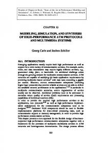
2. BEHAVIORAL MODELING OF PIPELINE ADCs USING SIMULINK® C-CODED S-FUNCTIONS Fig.1(a) shows the conceptual block diagram of a generic pipeline ADC, consisting of an arbitrary cascade of k stages and a Sampled-and-Hold (S/H) circuit at the front [1][2][11]. Each stage reIn
S/H
Stage 1
Stage 2
Stage k
n1
n2
nk
(a)
Digital Correction Logic Out
(b)
Nj ADC nj
Nj DAC
N
Σ
Gj
MDAC
Figure 1. Generic pipeline ADC architecture. (a) Conceptual block diagram; (b) structure of a single stage. †2. Indeed, the toolbox has been already extended to cover other converter topologies, such as full flash ADCs and current-steering Digital-to-Analog Converters (DACs).
†1. This work has been supported by the MEDEA+ (A110 MIDAS) Project.
0-7803-8834-8/05/$20.00 ©2005 IEEE.
problem is translated into a cost function minimization problem that can be evaluated through numerical methods. Evaluation of the cost function is normally performed by means of equations [11][12][14], so that very short computation times are obtained. As a drawback, this approach results in closed tools because equations must be changed every time the topology is changed. This paper aims at palliating this problem by using simulation instead of equations for cost function evaluation. To this end, a complete toolbox for the high-level synthesis of arbitrary pipeline ADCs has been developed in the MATLAB® environment [15]. The embedded simulator uses SIMULINK® S-functions [16] to model all required subcircuits including their main non-idealities. This approach considerably reduces computational costs as compared to using standard library blocks as in [13]. For all subcircuits, the accuracy of the behavioral models has been verified by HSPICE. Additionally, the toolbox includes an efficient hybrid optimizer which uses statistical techniques for design space exploration and deterministic techniques for fine tuning [17]. Other important features of the platform are a friendly Graphical User Interface (GUI), high flexibility for tool expansion†2 and wide signal processing capabilities [15]. As a case study on the use of the proposed synthesis tool, a 0.13µm CMOS 12-bit@80MS/s pipeline ADC for PLC is synthesized and designed. Different experiments show the effectiveness of the proposed methodology.
5609
solves partial code words of length n j , j = 1, …, k , which are all re-ordered and combined at the digital correction block to obtain the N-bit output of the converter. The inner structure of a pipeline stage comprises four blocks, as illustrated in Fig.1(b): a n flash sub-ADC with N j ≤ 2 j output codes, a sub-DAC with N j output levels, a substractor, and a S/H residue amplifier with gain G j . The latter three blocks are implemented in practice by a single subcircuit which is often referred to as Multiplying DAC (MDAC). All the critical blocks in the pipeline architecture, namely, S/H circuit, sub-ADCs and MDACs, have been modelled and coded in the proposed toolbox including their most important error mechanisms. As an illustration, Fig.2(a)†3 shows the conceptual schematic of a MDAC block which operates with two non-overlapped clock phases. Its model in the proposed toolbox includes the most critical error mechanisms which are computed according to the flow diagram in Fig.3. The flow graph has two branches corresponding to the two clock phases. During the sampling phase, the input-equivalent thermal noise, ( ∆v n ), is calculated and added to the voltage stored at the sampling capacitors C i . This is computed taking into account the finite switch on-resistance effects ( r on ). Next, an iterative procedure is started to calculate the output voltage v o by solving the equivalent circuit of Fig.2(b), which models the effects of finite and non-linear opamp DC-gain ( A v ( v x ) = G m ( v x ) ⁄ g ox ), opamp offset (not shown in Fig.2(b) for simplicity), non-linear capacitors, and the opamp dynamics (comprising both linear incomplete settling and slew-rate limitation), parasitic capacitances ( C p, C b, C load ), output range limitations and charge injection error. Note that a two-pole model (inva CN v in v ref
CN – 1
φ1 φ2
φ1 φ2
r on
C1
r on
CN
r on
Co
C'
φ 1 φ2
φ1 φ2 φ1 φ2 i–1 – v ref C i = 2 C u = C' = Cu C – v ref o
b1
C u : Unitary capacitor
vi
(b)
Co
b1
vo
+
C1
bN b N
φ1
v a r on C' r on
vo
Cp go
– Io
Cc Io
Yes
– Ioh
– v ref
Transient response Non-linear capacitors Output Saturation Transient response Charge Injection Error Output Saturation No Charge Injection Error No
(c)
r on C N ± v ref
va Cp
r on C' go
vo – Io
Cc Io g m (v h)
vh
g oh
C load
– Ioh
next MDAC
Residue amplification phase
0
g mh v a C h
End
Memorized input
Sampled phase
Residue amplification phase
0
5 Residue amplification phase
1
10 T (ns) Sampled phase
15
b 2 = ″0″ f s = 80MHz
20 C u = 0.5pF
Residue amplification phase
0 -1
v i = 0.5V b 1 = ″1″
Hspice Model
2
Ioh
Yes
Yes
cluding parameters g m, C load, g o, g mh, C h, g oh ) using Miller compensation ( C c ) has been developed for the opamp. During the residue-amplification phase, a similar procedure is applied to solve the equivalent circuit shown in Fig.2(c). As the value of state signals are important only at the end of each clock phase, a set of finite difference equations have been generated to describe the operation of real pipeline sub-circuits. These equations have been codified in C and incorporated as S-functions into the SIMULINK® environment [16]. This approach allows to drastically speed up the simulation CPU-time†4 (up to 2 orders of magnitude) as compared to previous approaches − based on the use of SIMULINK® elementary blocks [13]. Moreover, S-functions are more suitable for implementing a more detailed description of the circuit. As an example of the accuracy of the behavioral model, Fig.4 compares the transient response of a 2-bit MDAC for a constant input voltage by using HSPICE and our model showing a good agreement.
Vo (V)
± v ref
Opamp model
r on C o
Convergence
Convergence
Figure 3. Flow diagram of the MDAC model.
-0.5 r on C 1
Non-linear capacitors
Opamp finite and non-linear open-loop gain
0.5
gm h va Ch
Opamp finite and non-linear open-loop gain
Sampling error
Ioh
C load
No
Sampling phase
Calculate equivalent thermal noise ∆v n
vh
g oh
g m (v h)
v in
Va (V)
(a)
−
Input voltage
5
10 T (ns)
15
I o = 4mA g mh = 20mA/V I oh = 3mA
Hspice Model 0
g m = 0.5mA/V
C c = 0.1pF
20
Figure 2. MDAC (a) schematic, (b) equivalent circuit in sampling phase and (c) equivalent circuit in residue amplification phase.
Figure 4. Transient response of a 2-bit MDAC considering a constant input voltage: comparison between HSPICE and two-pole behavioral model.
†3. For illustration purposes, schematics are shown in its single-ended version, although actually the fully-differential structures have been modelled.
†4. A 32738-samples simulation takes 2-3 seconds. All simulations shown in this paper were done using a PC with an AMD XP2400 CPU@2GHz @512MB-RAM.
5610
3. DESCRIPTION OF THE SYNTHESIS TOOLBOX The models described above have been included in a SIMULINK®-based simulator. This simulator, used for performance evaluation, is combined with a statistical optimizer for design parameter selection as described below. 3.1 Optimization procedure Deterministic optimization methods, like those available in the MATLAB® standard distribution [15], are not suitable for synthesis purposes because they are strongly dependent on the initial conditions. However, initially designers may have little or no idea of an appropriate design point and hence, the optimization procedure is quickly trapped in a local minimum. For this reason, we developed an optimizer which combines an adaptive statistical optimization algorithm inspired in simulated annealing (local minima of the cost function can then be avoided) with a design-oriented formulation of the cost function (which accounts for the modulator performances). Moreover, an integrated approach is addressed: statistical techniques are applied for wide design space exploration whereas deterministic techniques are used for fine-tuning of best solutions found by the previous techniques. Unlike conventional simulated annealing procedures, in which the control parameter − commonly named temperature − follows a predefined temporal evolution pattern, the implemented global optimization algorithm dynamically adapts this temperature to approximate a predefined evolution pattern of the acceptance ratio (accepted movements / total number of iterations). This idea prevents excessively high temperatures which will make convergence difficult and inappropriately low temperatures which can make the algorithm to stuck on a local minimum. The amplitude of parameter movements through the design space is also synchronized with the temperature for improved convergence. The optimizer has been integrated in the MATLAB®/SIMULINK® platform by using the MATLAB® engine library [15], so that the optimization core runs in background while MATLAB® acts as a computation engine. The optimization core is very flexible, in so far as the cost function formulation is very versatile: multiple targets with several weights, constraints, dependent variables, and logarithmic grids are permitted. This optimization procedure has been extensively tested with design problems of Σ∆ modulators involving behavioral simulators [18] as well as electrical simulators [1]. 3.2 Implementation in the MATLAB® environment The proposed tool has been conceived as a MATLAB® toolbox for the simulation and synthesis of Nyquist-rate data converters, including flash, pipeline ADCs and current-steering DACs. Fig.5
shows some parts of the toolbox comprising a GUI to allow the designer to browse through all steps of the simulation, synthesis and post-processing of results.
4. CASE STUDY: A 12-bit@80MS/s ADC FOR PLC In order to illustrate the capabilities of the proposed toolbox, the high-level design of a 0.13µm CMOS 12-bit@80MS/s pipeline ADC for PLC will be described. The specifications are shown in Table 1 and the objective consists on achieving those specifications with the minimum area and power consumption. In addition, this design is planned to be implemented without using calibration. For that reason, capacitor mismatch is a critical issue. In fact, this limitation forces us to optimize the capacitor sizes not only in terms of thermal noise and dynamics considerations but also in terms of minimum capacitance area needed to achieve the required mismatch. Another critical parameter considered in the optimization is the resolution per stage. Taking into account these factors, a wide exploration of several architectures has been carried out with the proposed synthesis toolbox. The optimum architecture was a 7-stage pipeline with the next resolution-per-stage: 3-2-3-2-3-3-2. Redundant sign digit coding was used in order to relax the requirements for the comparators in the flash quantizers. The results of the high-level synthesis for the first stages as well as the requirements for the opamps are summarized in Table 2. The optimization procedure for a given architecture required about 4000 iterations of 16384-clock cycles taking about 2 hours of CPU-time. Finally, Table 3 shows a summary of the converter performance from where it can be deduced that the specifications are fully satisfied. MonteCarlo analysis has been carried out taking into count both capacitor and resistor mismatch in order to characterize typical and worst cases of different figures. As an illustration, Fig.6(a) shows an histogram of a MonteCarlo analysis of the MTPR ((case (a) in Table 1)) comprising 1000 simulations and Fig.6(b) shows the output spectrum of one of those simulations.
CONCLUSIONS MATLAB®
A complete toolbox for the high-level synthesis and verification of pipeline ADCs has been described. The combination of an efficient SIMULINK®-based time-domain behavioral simulator and an advanced statistical optimizer allows to efficiently map system-level specifications into building-block specifications in reasonable computation times. Critical design issues such as the resolution-per-stage are optimized in terms of power consumption and silicon area. As a case study, a 0.13µm CMOS 12bit@80MS/s ADC for PLC front-end has been designed and analysed using the proposed toolbox. Table 1: Specifications for pipeline ADC Specifications: 12bit@80MS/s
Figure 5. Some parts of the data converter MATLAB® synthesis toolbox.
5611
Multi-Tone Power Ratio (MTPR) (a) 15 tones on-1 tone off (b) 120 tones on - 8 tones off (c) 240 tones on - 16 tones off Effective Number Of Bits (ENOB) Differential Input Range Power Supply
≥ ≥
56dB
9.2 bits 2 Vp-p 3.3V
REFERENCES [1] A. Rodríguez-Vázquez, F. Medeiro and E. Janssens (Editors): CMOS Telecom Data Converters. Kluwer Academic Publishers, 2003. [2] M. Gustavsson, J. J. Wikner and N. N. Tan: CMOS Data Converters for Communications. Kluwer Academic Publishers, 2000. [3] G. G. E. Gielen and R. A. Rutenbar: “Computer-Aided Design of Analog and Mixed-Signal Integrated Circuits”. Proceedings of the IEEE, Vol. 88, pp. 1825-1852, December 2000. [4] K. Uyttenhove, J. Vandenbussche, E. Lauwers, G. G. E. Gielen and M. S. J. Steyaert: “Design Techniques and Implementation of an 8-bit 200-MS/s
Table 2: High-level synthesis for the pipeline ADC Requirement
Opamp
135 >60
1st. stage (3 bits)
81
2nd. stage (2 bits)
Noise PSD (nV/ Hz ) Comparators Offset (mV) Comparators Hysteresis (mV) Unitary capacitor (pF) Switch on-resistance (Ω) Eq. load (pF) Slew-Rate (V/µs) MDAC GB (MHz) DC-gain (dB)
72
3rd. stage (3 bits)