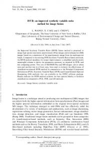
couplers, this kind of devices have an extra compact footprint of below 15 μmÃ15 .... are shown below; (c) Variation of splitting index S and IL as a function of D.
This article has been accepted for publication in a future issue of this journal, but has not been fully edited. Content may change prior to final publication. Citation information: DOI 10.1109/JPHOT.2018.2832188, IEEE Photonics Journal
Broadband 1×3 Couplers with Variable Splitting Ratio using Cascaded Step-Size MMI Ye Tian1, Jifang Qiu1, Mingbin Yu2, Zhuili Huang1, Yingying Qiao1, Zhenli Dong1, Jian Wu1 1Key
Laboratory of Information Photonics and Optical Communications, Beijing University of Posts and Telecommunications, Beijing, 100876, China 2Shanghai
Institute of Microsystem and Information Technology, Chinese Academy of Sciences, Shanghai, 200050, China
Abstract: In this paper, we propose and fabricated a novel scheme of SOI-based 1×3 coupler with variable splitting ratio. The coupler consists of two cascaded MMI with different sizes, and a wide range of splitting ratios from 1:0.1:1 to 1:18:1 can be achieved by modifying the size of the first-step MMI. Using the structure of cascaded step-size MMI, this kind of device has a compact footprint of below 15 μm×15 μm and simple fabrication process. Meanwhile, the simulation analyses prove that the proposed couplers have a large operation bandwidth above 60 nm and be robust to the fabrication errors. Couplers with several splitting ratios were fabricated and well measured. Based on the measurement results, the splitting ratios of fabricated couplers from 1:0.67:1 to 1:18:1 can be achieved, and stable performance with the transmission efficiencies above 80% can be maintained over 50 nm wavelength range, which is the largest operation bandwidth to the best of our knowledge. Index Terms: Optical couplers, silicon photonics.
1. Introduction In recent years, photonic integrated circuits (PICs) based on Silicon-on-insulator (SOI) platform has attracted great attention due to the high level of integration density and its compatible fabrication process with integrated electronics [1]. Among the integrated components, power couplers are one of the essential items in PICs. So far, a lot of works on 1×2 couplers have been done and the arbitrary ratios can be achieved by a number of methods [2-5]. However, the research of a multi-output splitter with variable splitting ratios is still at early stage, due to the increased design complexity. A 1×3 coupler with variable splitting ratios would be highly advantageous for several applications, such as signal quality monitor [6], quantization resolution enhancement [7], etc. To achieve this function, various structures have been proposed, including directional couplers (DCs), photonic crystals (PhCs) [8,9], multi-layer structures [10], QR code-like structures [11] and multimode interference (MMI) couplers. Among them, MMI couplers, which utilize the principle of self-imaging effect [12], has been considered as a preferred candidate because of its compact footprint, wavelength insensitivity, low insertion loss and high fabrication tolerance. However, a traditional MMI usually divides the optical power equally according to the self-imaging theory, or few splitting ratios can be obtained by adjusting the positions of input and outputs ports [13]. To obtain a wide range of splitting ratios, a butterfly-shaped 1×3 MMI was designed and fabricated in Refs. [14]. However, the footprint is large as hundreds of microns, which may lead to the reduction of stability. MMI couplers with electro-optic tuning element is an alternative that allows the realization of tunable splitting ratios [15]. However, the footprint of this kind of device has to be large enough to avoid the thermal crosstalk, and the cost may be increased as the electro-optic tuning element requires more fabrication steps. In this paper, we propose a novel 1×3 MMI coupler with variable splitting ratios. By cascading two MMI couplers of different sizes, and modifying the structure of first-step MMI, a wide range of splitting ratios can be achieved. Compared to other 1×3 couplers, this kind of devices have an extra compact footprint of below 15 μm×15 μm, a large operation bandwidth above 60 nm and simple fabrication process (one-step etch). Meanwhile, the proposed couplers are robust to the fabrication errors. Then, several couplers with specific splitting ratios (from 1:0.67:1 to 1:18:1) were chosen to be fabricated on a SOI platform, the measurement results verify the high transmission efficiency of above 80% (equivalent to insertion losses below -1 dB) in a large operation bandwidth over 50 nm. Lowest insertion loss is around 0.2 dB at a wavelength of 1550 nm.
2. Principle 2.1 Analysis for varying splitting ratios in MMI For a MMI of width W and length L, according to the eigenmode decomposition theory [12], any input light distribution fin(x) can be decomposed into the eigenmodes in the MMI. Therefore, the output light distribution fout(x) is actually the superposition of each eigenmode at length L, as shown in Fig.1. The strongly guided eigenmodes of MMI section have the form:
Emi ( x) sin((i 1)
x ) W
with i 0, 1, 2, ....
(1)
where i represents the order number of eigenmodes. Using a spatial Fourier decomposition, fin(x) can be rewritten as a superposition the infiniteandnumber of are strongly guided i 1943-0655 (c) 2018 of IEEE. Translations content mining permitted for academic eigenmodes research only. Personalwith use is coefficient also permitted, butarepublication/redistribution requires IEEE permission. See http://www.ieee.org/publications_standards/publications/rights/index.html for more information.
This article has been accepted for publication in a future issue of this journal, but has not been fully edited. Content may change prior to final publication. Citation information: DOI 10.1109/JPHOT.2018.2832188, IEEE Photonics Journal
fin ( x) ai Emi ( x),
with 0