Buffer Delay Change in the Presence of Power and Ground Noise Lauren Hui Chen*, Malgorzata Marek-Sadowska**, Forrest Brewer** *Synopsys Inc., Mountain View, CA, USA ** Electrical and Computer Engineering Department, University of California, Santa Barbara, CA 93106, USA *
[email protected], **{mms, forrest}@ece.ucsb.edu
ABSTRACT
them, [9] proposes an optimum multistage buffer design to drive long uniform lines. [7] and [15] consider simultaneous buffer insertion and wire sizing for timing optimization. [1] presents comprehensive buffer insertion techniques for noise and delay optimization. Because of the buffer/repeaters’ preponderance in number, use in heavily loaded nets, and use in clock and timing circuits, buffer delays account for a large percentage of all critical timing nets in a design. In some of these applications, total timing uncertainty (not just worstcase delay) is important. Disturbance of the buffer delay will affect the type, number and position of buffers that optimize the interconnect delay. Therefore, it is essential to take the change of delay into consideration in order to adjust the solution for timing optimization. At the same time, scaling of power supply levels and improving transconductance of devices have increased the sensitivity of buffers to supplylevel-induced delays. Finally, increases in chip-level design scales and modern packaging strategies such as bump bonding have localized supply variations so that buffers in one set of supply levels are driving buffers in another zone with different supply levels. Since power loading is logic switching-dependent and supply sources are localized, power and ground levels need not be inversely correlated as is typical in a wire bonded die.
Variations of power and ground levels affect VLSI circuit performance. Trends in device technology and in packaging have necessitated a revision in conventional delay models. In particular, simple scalable models are needed to predict delays in the presence of uncorrelated power and ground noise. In this paper, we analyze the effect of such noise on signal propagation through a buffer and present simple, closed-form formulas to estimate the corresponding change of delay. The model captures both positive (slowdown) and negative (speedup) delay changes. It is consistent with shortchannel MOSFET behavior, including carrier velocity saturation effects. An application shows that repeater chains using buffers instead of inherently faster inverters tend to have superior supply-level-induced jitter characteristics. The expressions can be used in any existing circuit performance optimization design flow or can be combined into any delay calculations as a correction factor.
Categories & Subject Descriptors: [ComputerAided Engineering]: Computer-aided design (CAD).
General Terms: Algorithms. Keywords: Power and ground noise, differential mode noise, common mode noise, incremental delay change.
Under such conditions, power-level-induced delay changes may either increase or decrease the effective delay of a buffer, and successive stages may or may not accumulate incremental delays. One must consider both power and ground levels at the signal source and at the current buffer to derive an equivalent delay change. This value can be substantially smaller than that predicted by superposing ground-bounce and power level changes [3][5][10][20][21]. The superposition approximation works well only if the variations in the power distribution network are mirrored in the ground network. However, due to changes in packaging technology and the number of pins that can feasibly be devoted to power and ground connections, no single parasitic dominates the noise on the power and ground nets. Yet another trend in technology is the relative reduction of gate parasitics compared to those from the interconnection network. The net effect of this is de-correlation of the power and ground voltage variations which in turn make delay variations much more complex. In particular, the worst-case
1. INTRODUCTION This paper describes a new model for the change in buffer delay caused by both power and ground supply level variations and level variations between stages in sequences of repeaters. These delay changes are a large component of the total timing jitter for a signal where the jitter accounts for all noise sources such as substrate noise and coupling noise as well as power level noise. There is a substantial amount of previous work in this area, notably papers: [4][6][13][14] [19]. However, for several reasons described below, we believe that the problem bears re-examination and a renewed effort to create a fast, simple model suitable for mass implementation in a modern design flow. Growth in design sizes and scaling of interconnections have led to the requirement for insertion of very large numbers of buffer/repeaters in recent designs [1][7][9][15]. Among
1
delay caused by power noise may not occur simultaneously with the worst-case delay due to ground noise, and the superposition may cause a substantial overestimation. Second, the delay effects of common mode voltage shifts will be shown to be larger in scale than equivalent differential mode changes. (Differential mode voltage shifts are the most commonly studied model). Lastly, changes in power distribution and clocking strategies, and the potential for future changes, create the need for a timing model which is independent of common assumptions about power level noise sources. We do assume that large scale power level changes result from an ensemble effect of many devices at a variety of differing slew rates. However, in a practical design there must always be some amount of local decoupling capacitance (both parasitic and added). This capacitance limits the magnitude of the highest speed noise excursions. (This cannot be done in later stages of the power network design because of inductance in both the physical network and the packaged capacitors). We therefore assume that the remaining large magnitude noise excursions occur at a somewhat slower time scale than the typical switching transitions in buffers meeting common design requirements.
denote the variation of power supply and ground, respectively. ′
∆V dd = V dd – V dd (power noise) ′
′
∆V ss = V ss – V ss = V ss ( V ss = 0 ) (ground noise)
(1) (2)
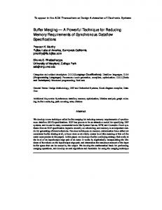
In small-scale wire-bond packaging styles, a dominant supply level noise source is bond wire inductance in the package. Neglecting I/O current drives, the power and ground noise of the chip due to simultaneous switching typically follows an inverse pattern, and ∆Vdd is often symmetric to ∆Vss. However, in modern bump-bonded and low-inductance package styles, the package distributes power over the whole area of the chip (figure 1). Every bump connects to an underlying local power/ground network. To save chip metallization area and improve density, global power distribution metal is reduced in preference to thicker package distribution layers. Increasing design scales causes an increase in long wire loading, and in more wires connecting between different power domains. Logic-level-dependent currents flow between such blocks, causing asymmetric power and ground noise within a block. This noise is increased by the inclusion (within a bump block) of long wire repeater buffers which are often added in a post-placement timing optimization step.
In the following, we analyze the effect of P/G (power/ ground) noise on buffer delay, and present linear, closedform formulas for the corresponding incremental changes in delay based on a short-channel transistor model. The expressions simultaneously model both the power supply and ground levels, resulting in positive (slowdown) or negative (speedup) delay changes. These expressions are intended for inclusion in timing analysis tools and statistical delay estimators as corrections to nominal delay models that account for other effects. The expressions make few assumptions about the specific shape of the P/G noise waveform. Furthermore, they are shown to be largely independent of the buffer load circuit structure, increasing their applicability.
Figure 1 shows a simple circuit which uses bump-bond packaging. Each block is defined by the subcircuit supplied by a pair of bumps (Vdd/Vss). Suppose that the cells A to E have transitions. Switching of the buffers A, B and D has a ′(1) symmetric effect on the power and ground noise ( ∆V dd and ′(1) ∆V ss ), because they drive loads (consisting largely of parasitic interconnect capacitance) within the same block. On the other hand, switching of the C and E buffers has a ′(1) ′(1) non-symmetric effect on ∆V dd and ∆V ss , because they drive loads which are outside of block 1, causing different switching currents to flow through the power and ground ports of block 1. Since wires leaving a block are likely to be physically long, these currents are proportionally large. In general, there is little reason for the currents flowing out of the block via loads to cancel.
The rest of the paper is organized as follows: sections 2-3 define P/G noise, buffer delay nomenclature, and illustrate the P/G-noise-induced buffer delay change. Section 4 presents our new model. Section 5 demonstrates the accuracy and fidelity of the model. Applications of the model and concluding remarks are presented in sections 67. Detailed derivations are given in Appendices A and B.
2.2 Incremental buffer delay change To allow reference to previous work, it is necessary to formally define the model for buffer delay, as the measurement levels are subject to noise.
2. BUFFER DELAY CONVENTIONS
Without loss of generality, we define a buffer’s ideal delay as the time interval between its input and output voltage reaching 50% of the power supply level. Figure 2 illustrates the definition for an inverter delay given ideal power supply and ground levels. tpHL is the high-to-low delay when the input of the inverter has a rising transition. The input and output transition times are tr and toT, respectively. Other time values are: ti5, to5, to1 and to9, which are times when the
A buffer is a chain of tapered inverters. Here, we consider buffers consisting of one inverter or two inverters.
2.1 Variation of Vdd and Vss We use Vdd, Vss, Vi (input), Vin (adjusted input), Vo (output), Vout (adjusted output), etc. to represent values related to the ideal power and ground levels, and we use Vdd’, Vss’, Vi’, Vin’, Vo’, Vout’, etc. to represent the corresponding values in the presence of power and ground noise. ∆Vdd and ∆Vss 2
Vdd
Vdd
Vdd Package Redistribution Layer / Plane
VTR
’(1)
B D
voltage
Local Redistribution Parasitics ’(2) Vdd
Vdd A
0.9Vdd
Vdd Pin Parasitics
’(1)
Vo (output)
tpHL
0.5Vdd VD0
C
Vtn
BLOCK 2
E
0.1Vdd
BLOCK 1 Vss
Vi (input)
0.8toT
Vss
V tn --------t V dd r
’(2)
Vss Local Redistribution Parasitics
region
Vss Package Redistribution Layer / Plane
1 NMOS CUT
Vss Pin Parasitics
to9 tr to5 tD0
ti5
2 SAT
time
to1
3 SAT
4 LIN
Figure 2. Ideal inverter transition and nomenclature Vss ′
′
′
′
′
′
′
′
′
′
′
′
V o1 = V ss + 0.1 ( V dd – V ss )
Figure 1. Power distribution in bump-bond packaging
V o5 = V ss + 0.5 ( V dd – V ss )
input or output voltage reaches 50%, 10%, and 90% of Vdd, respectively. t pHL = t o5 – t i5 t o1 – t o9 t oT = ------------------0.8
V o9 = V ss + 0.9 ( V dd – V ss )
The disturbed high-to-low delay and slope are given by:
(3)
′( j)
′( j)
′( j)
′( j)
′( j)
t pHL = t o5 – t i5
(4)
t o1 – t o9 ′( j) t oT = ----------------------0.8 where j = 1, 2, 3, 4 , indicating four different definitions of
Figure 3 (a) and (b) illustrate the delay and slope when there is a P/G noise. In figure 3(a), we assume a bump-bond packaging technique, in which every bump has a small power/ground network, relatively independent of the others. Therefore the low and high voltage levels of the input transition ( V ss → V dd ) are independent of the change of power supply and ground level for the buffer. The ′(1) ′(2) corresponding buffer delays are t pHL and t pHL . In figure 3(b), conventional wire-bond packaging technique is assumed. For such a technique, the dominant noise on the power supply and ground level is often due to the wiring inductance in the package, so the whole chip’s power and ground noises are synchronized. Therefore, the voltage level ′ ′ of the input transition ( V ss → V dd ) will be the same as that ′(3) of the buffer. The corresponding buffer delays are t pHL and ′(4) t pHL . Because of power supply and ground level changes, we are interested in delay measured at different voltage ′(1) levels: the 50% point between the ideal Vdd and Vss ( t pHL ′(3) and t pHL ), and the 50% point between the disturbed Vdd’ ′(2) ′(4) and Vss’ ( t pHL and t pHL ). Hence we have four types of disturbed buffer delays, corresponding to four types of buffer delay changes.
the disturbed buffer delay and output slope illustrated in figure 3 (a) & (b). ′(1)
′(2)
′(1)
′(2)
In figure 3(a) we have t o1 = t o1 and t o9 = t o9 . In figure ′(3)
′(4)
′(3)
′(4)
3(b) we have t o1 = t o1 and t o9 = t o9 . Therefore, ′(1)
′(2)
′(3)
′(4)
t oT = t oT , t oT = t oT
With a rising transition at the input, the changes of delay and output transition time are defined as follows: ( j)
′( j)
∆t pHL = t pHL – t pHL ( j)
′( j)
∆t oT = t oT – t oT
The results shown in figure 5 are according to the first type of delay definition with j = 1.
3. P/G NOISE DELAY EFFECTS The changes of power supply and ground level affect signal propagation through an inverter in several different ways, which will be discussed in this section.
The special output voltage points are defined as follows:
3
,
,
Vdd
Vdd
Vo9 Vdd
Vo9 Vdd
,
,
,
Vdd Vss
0.5Vdd
,
’ Vdd
’ Vdd ’ Vss
(1)
tpHL
’ Vdd ’ Vss
0.5Vdd
,
’ Vdd
’ Vdd ’ Vss
(3)
tpHL
’ Vss
’ 0.8toT
,
Vo1
,
(4)
tpHL
, Vo5
’ Vss
’ 0.8toT
,
Vo1
Vo (output)
,
(2)
voltage
voltage
,
,
Vi (input)
Vo (output)
tpHL
, Vo5
,
,
Vi (input)
,
Vss Vss
,(1) ,(2)
,
,(2) ,(1)
ti5 ti5 to9 to5 to5
,
to1
Vss Vss
time
,(3) ,(4)
,
,
(4)
,
(3)
ti5 ti5 to9 to5 to5
(a)
,
time
to1
(b)
Figure 3. Notation for disturbed delay and slope
3.1 Differential mode noise
(P)
We define the differential mode noise (DMN) ∆Vdif as:
VGS
′
∆V dif = V dif – V dif = ∆V dd – ∆V ss
Vi
′
Vss , Vdd
Vdd
∆Vdd
|Vtp|
Vss
∆Vss
Vtn
N
Vtn
,
(shift)
|Vtp |
(b)
N’
,
Vss
|Vtp|
P’ P
The differential mode noise ∆Vdif may become positive or negative, depending on the directions and relative amplitudes of ∆Vdd and ∆Vss. The voltage difference (Vdif) between power supply and ground level determines how fast the buffer charges/discharges its capacitive load, so it affects the delay and the transition time of the buffer output. The ′ larger the difference ( V dif > V dif ⇒ ∆V dif > 0 ), the faster the output charging/discharging and the smaller the buffer delay ′ (t pHL < t pHL ⇒ ∆t pHL < 0 ), which is stated in observation 1.
(shift) Vtn
,
tn tn tp tp
Figure 4. Threshold shift of an inverter
3.2 Common mode noise We define the common mode noise (CMN) ∆Vcom as:
Observation1: The buffer delay change is linearly dependent on the differential mode noise (DMN), as will be shown in section 4: = – k d ⋅ ∆V dif = – k d ⋅ ( ∆V dd – ∆V ss )
(N )
V GS = V i – V ss
(N) VGS
We have observed through HSpice simulations that the voltage difference (Vdif) between the power supply and ground level affects the inverter delay (tpHL/tpLH), which is the inverter’s ability to propagate signals. Similarly, the change of the above difference (∆Vdif) affects the change of delay (∆tpHL/∆tpLH).
DMN
(a)
′
V dif = V dd – V ss and V dif = V dd – V ss
∆t pHL
V GS = V i – V dd
Vo wire load
where ′
(P)
Vdd
∆V com = ∆V dd + ∆V ss
CMN modifies the effective switching threshold of the gate. The threshold shift changes the gate delay as illustrated in figure 4. Figure 4(a) shows a rising transition arriving at the buffer. Figure 4(b) illustrates the gate threshold shift and the corresponding delay change caused by the power and ground variations.
(5)
where kd is a positive constant dependent on the device and technology parameters, the input transition times, and the gate load. The expression of kd can be found from equation (A5) in Appendix B. Similar effects hold for both high-tolow delay ∆tpHL and low-to-high delay ∆tpLH.
In figure 4(b), N and P are the original points when the NFET switches from cutoff to saturation region and PFET switches from saturation to cutoff, respectively. The
4
corresponding switching times are indicated tn and tp. For noise of limited amplitude, the transistor thresholds (Vtn and Vtp) do not change significantly, namely, ′(N )
′
V GS
= V i – V ss = V tn > 0
CUT
′(P)
V GS
For a rising transition, the effective switching threshold of an inverter is set by the current balance of the two active transistors. For positive common mode noise, this switching threshold is higher, and therefore it is reached later by the rising transition. Thus the delay is increased even though the voltage across the inverter, and hence the current drive, remains constant.
′
CUT
= V i – V dd = V tp < 0
For a falling transition, the effective switching threshold of the gate rises, so that the threshold voltage level is reached earlier, and the effective gate delay decreases. This effect occurs even if the differential mode noise is zero, as it is the switching level - not the current drive - that is altered by the common mode noise.
This causes a shift of the NFET and PFET switching points from N and P to N’ and P’. The corresponding switching time shifts to tn’ and tp’, respectively. The points N’ and P’ can be mapped to shifted thresholds in figure 4(a) with ideal power supply and ground level: (N )
V GS
( shift )
CUT
( shift )
(P)
V GS
We note an analogy here: a rising input transition with positive common mode noise can be thought of as climbing a rising mountain, which takes more time than climbing a mountain of initially the same, yet stationary, dimensions. A falling input transition with the same positive common mode noise is analogous to going downhill when the bottom of the mountain rises, which takes less time than descending a corresponding fixed dimensions mountain.
= V i – V ss = V tn
CUT
= V i – V dd = V tp
We observe in figure 4(b) that: ( shift )
> V tn ⇒ t n > t n ⇒ increasing delay
( shift )
> V tp ⇒ t p > t p ⇒ increasing delay
∆V ss > 0 ⇒ V tn
∆V dd > 0 ⇒ V tp
′
′
Therefore, common mode noise has a different effect on rising and falling transitions.
Obviously, it takes more time for the NFET transistor to be turned on and PFET to be turned off when both power supply and ground level increase.
3.3 Loading effects Both differential mode noise (DMN) and common mode noise (CMN) change buffer delays. Since the delay change can be of either sign, the noise sources need to be modeled together. Figure 5 shows alternative load configurations and the corresponding simulated delay change (both rising and falling transition) in 0.18µm technology. Note: ∆delay = 0 when ∆Vdd = ∆Vss = 0.
On the other hand, when power supply and ground level decrease, we have ( shift )
< V tn ⇒ t n < t n ⇒ decreasing delay
( shift )
< V tp ⇒ t p < t p ⇒ decreasing delay
∆V ss < 0 ⇒ V tn
∆V dd < 0 ⇒ V tp
′
′
Hence, it takes less time for the NFET transistor to be turned on and PFET to be turned off for decreased power and ground level.
In figure 5 (a), the wire load of the inverter is a distributed RC tree network, including vias, extracted from the layout of a real circuit. In figure 5 (b), the wire load is simplified to an RC π-model. In figure 5 (c), the wire load is further simplified to a single resistor plus a single capacitor. In figure 5 (d), an effective loading capacitor is used to replace the inverter’s output load. These simplified wire-load models in figures 5(b)-(d) can be obtained using the methods described in [16]. The delay is measured when its input (Vi) and output (Vo / Vo’ / Vo” / Vo”’) voltage reach 50% of the ideal power supply voltage, respectively. The range for the power and ground noise is from -20% (-0.36 volt) to 20% (0.36 volt) of the power supply voltage, which is set to 1.8 volt for the selected technology. The range for the change of delay is from -30ps to 30ps.
Therefore, we make the following observation: Observation 2: For an input with a rising transition, the dependency between the common mode noise (CMN) and the buffer delay change can be expressed by: ∆t pHL
CMN
= k cr ⋅ ∆V com = k cr ⋅ ( ∆V dd + ∆V ss )
(6)
where kcr is a positive constant determined by the device and technology parameters, input transition time, and the gate load. The expression of kcr can be found from equation (A5) in Appendix B. Similarly, for an input with a falling transition, the dependency between the common mode noise (CMN) and the buffer delay change can be expressed by: ∆t pLH
CMN
= – k cf ⋅ ∆V com = – k cf ⋅ ( ∆V dd + ∆V ss )
It is interesting to note that each of the four wire load models displays a linear relationship between the change of power/ground level and the change of inverter delay. Furthermore, the linearity improves when the change of power and ground level is smaller than 20%. In practical designs, the tolerable range for the power and ground levels
(7)
where kcf ia a positive constant determined by the device and technology parameters, input transition time, and the gate load. 5
∆tpLH
∆tpHL Vi
Vo o
q
0.4
∆V c
(a) Distributed RC load (extracted from layout)
0.4
0 -0.4
om
-0.4
om
∆V dif
∆tpLH
0.4
0.4
∆V c
0 -0.4
om
Vo” o”
∆V c
0
∆V dif
om
0 0.4 0.4
∆V dif
∆tpLH
C3
0.4
0.4
0
∆V c
-0.4
om
-0.4
-0.4
-0.4 0
∆V c
0
∆V dif
om
∆tpHL
Vo’” o’”
-0.4
-0.4
0 -0.4
∆tpHL
R2
(c) Single RC load
Vi
0.4 0.4
C1
C2
(b) π-model load
Vi
0
R1
Vo’ o’
0
∆V c
∆V dif
∆tpHL Vi
-0.4
-0.4
0
0 0.4 0.4
∆V dif
∆tpLH
Ceff
(d) Effective capacitance load
0.4
0.4
∆V c
0 -0.4
om
0 -0.4
∆V dif
-0.4
-0.4
∆V c
0
om
0 0.4 0.4
∆V dif
Figure 5. Buffer delay change induced by P/G noise is usually less than ± 10% .Thus, the CMN and DMNinduced delays can be superposed as noted below.
where k1r, k1f, k2r and k2f are positive constants dependent only on input transition time, gate load, and the device and technology parameters. The actual expressions can be found from equations (11) and (14) in section 4.2, based on the theoretical model.
Observation 3: For a rising input transition and any of the wire load models described in figure 5, the incremental change of buffer delay due to P/G noise is expressed as: ∆t pHL = k 1r ⋅ ( ∆V dd + ∆V ss ) – k 2r ⋅ ( ∆V dd – ∆V ss )
Observation 3 brings in two related observations.
(8)
Observation 4: Buffer delay change is more sensitive to common mode noise than to differential mode noise for deep submicron designs, and may be dominated by common mode noise in some instances. This is indicated by the fact that the slope along the ∆Vcom direction is much steeper
A similar result applies to a falling input transition: ∆t pLH = – k 1 f ⋅ ( ∆V dd + ∆V ss ) – k 2 f ⋅ ( ∆V dd – ∆V ss )
(9)
6
than the slope along the ∆Vdif direction in figure 5. It also indicates k1r > k2r and k1f > k2f in equations (8) and (9). This will be further discussed in section 4.4.
4. THEORETICAL MODEL
Observation 5: Common mode noise has different effects on rising and falling transitions. As shown in figure 5, for a rising transition, with the increase of ∆Vcom from -0.4 to 0.4 volt, delay change increases. However, for a falling transition, it is with the decrease of ∆Vcom from 0.4 to -0.4 volt that the delay change increases. This is indicated by different signs associated with (∆Vdd + ∆Vss) in equations (8) and (9): positive for a rising and negative for a falling transition.
In deep submicron circuits, carrier velocity saturation effects predominate. To capture these effects when deriving the signal transition delay and slope values in the presence of power and ground variations, we use the short channel alpha-power law MOSFET model [17].
4.1 Inverter model
From Figure 6, we have the following nodal equation: In + I p = Ic
where
Observation 3 indicates that an appropriate simplified wire load model can be used for delay modeling of the buffer itself. With appropriate techniques [2][8][11][16], the distributed RC load of a gate can be simplified into the nearly equivalent π-model shown in figure 5(b). This πmodel is further simplified into an effective capacitance load, shown in figure 5(d), by equating the average currents for the two load models. Such a capacitance model is inaccurate when the gate is behaving like a resistor [16]. This inaccuracy occurs primarily in the tail portion of the output waveform. However, for our purposes, the buffer delay is measured at the midpoint of the logic swing. Therefore, the inaccuracy in the gate delay (not the wire delay) caused by the effective capacitance model is relatively small, usually less than 5% for the technologies reported in the results.
d ( V o – V ss ) I c = – C L ----------------------------dt
In deep submicron circuits the signal transitions are fast, so we can ignore the short circuit current [17][18]. (For the technologies reported in the results, short circuit errors amounted to less than 5% for incremental delay and 20% for incremental transition time, over all simulated cases.) For a rising transition at the inverter input, short circuit current from the NFET is negligible. The current flowing through NFET (In) is computed from the following equation [17]: 0 I n = I D1 ( I D1 ⁄ V D1 ) ⋅ V DS
The output voltage at node o in figure 5 (a) can be approximated by the voltage at node o’ in figure 5 (b), o” in figure 5 (c) and o”’ in figure 5 (d): ′
″
( V GS ≤ V tn ) ( CUT ) ( V DS ≥ V D1 ) ( SAT )
(10)
( V DS < V D1 ) ( LIN )
where V in – V tn α V GS – V tn α I D1 = I D0 ------------------------ = I D0 ----------------------- V dd – V tn V dd – V tn
′″
Vo ≈ Vo ≈ Vo ≈ Vo
However, the voltage at node q is different from that of node o:
V in – V tn α ⁄ 2 V GS – V tn α ⁄ 2 = V D0 ----------------------- V D1 = V D0 ------------------------ V dd – V tn V dd – V tn
Vq ≠ Vo
CUT, SAT, and LIN represent cutoff, saturation, and linear modes of operation, respectively. And:
The simplified wire load model is only used to characterize the interconnect’s driving point (node o) delay, not the receiving node (node q) delay. A variety of techniques exist [5][11] in order to model the interconnect delay. In this paper, we focus only on the buffer delay characterization which is typically half of the total wire delay for optimized long wires.
V in = V i – V ss = V GS V out = V o – V ss = V DS
The above alpha-power law model is based on four parameters: α (velocity saturation index), Vtn (threshold
Power and ground noise can either be correlated or largely independent depending on the relative magnitude of the power distribution parasitics and the relative number and activity of signals crossing between power distribution blocks. This noise contributes to the local buffer/inverter delay in a complex way which can either increase or decrease the signal delay. For application in performance estimation, optimization, or analysis, it is useful to develop simple models which can be quickly evaluated and which can be linked to theoretical device models.
Vdd
Vi
Ip
Vo
In Ic CL Vss
Vss
Figure 6. Propagation of a transition 7
( j)
voltage), ID0 (drain current at VGS = VDS = Vdd), VDO (drain saturation voltage at VGS = Vdd). For MOSFET in current technology, typical values for these parameters are: α = 1 ∼ 1.2 , V tn ⁄ V dd ≈ 0.2 , and V D0 ≤ 0.6V dd . We assume that for a given transistor with a given loading capacitance, the above four values remain unchanged with a small disturbance of power supply and ground levels.
( j)
( j)
⋅ ∆V com –
( j)
⋅ ∆V dif
( j)
= k 1n ⋅ ( ∆V dd + ∆V ss ) – k 2n ⋅ ( ∆V dd – ∆V ss ) ( j)
( j)
( j)
( j)
( j)
( j)
( j)
( j)
(15)
( j)
( j)
( j)
( j)
∆t pHL = k 1n ⋅ ( ∆V dd + ∆V ss ) – k 2n ⋅ ( ∆V dd – ∆V ss ) + ∆t r ⋅ f ds ( j)
where f ds is a function of P/G noise. For example, for the first type of delay change, we have:
(11)
∆V ss 1 (1) 1 f ds = --- – ------------- ⋅ 1 – ----------- – vT V dd 2 1+α
which can be further simplified to: ′(1) ′(1) ′(1) ′(1) ∆t pHL = k 1n ⋅ ( ∆V dd + ∆V ss ) – k 2n ⋅ ( ∆V dd – ∆V ss ) + k 5n (16)
where
(13)
CL t r + ∆t r ′(1) -, - + ----------k 1n = -----------------------------2V dd ( 1 + α ) 2I D0
For the four types of delays defined in figure 3, we obtained the following coefficients: tr tr CL CL (1) (1) k 1n = ------------------------------ + ----------- – -----------, k = -----------------------------2V dd ( 1 + α ) 2I D0 2n 2V dd ( 1 + α ) 2I D0
t r + ∆t r CL ′(1) k 2n = ------------------------------ – ----------2V dd ( 1 + α ) 2I D0
tr tr CL α (2) (2) ⋅ ------------- , k k 1n = – -----------= ------------------------------ – ----------2V dd 1 + α 2n 2V dd ( 1 + α ) 2I D0
′(1) 1 1 – vT k 5n = ∆t r ⋅ --- – -------------- 2 1 + α
vT ⋅ t r CL CL (3) (3) k 1n = -----------, k = --------------------------– ----------2I D0 2n ( 1 + α )V dd 2I D0 vT ⋅ t r CL (4) (4) k 1n = 0 , k 2n = ----------- – --------------------------2I D0 ( 1 + α )V dd
( j)
Under certain circumstances, the input transition time can be changed by the P/G noise. In other words, ∆t r ≠ 0 , and ′ t r = t r + ∆t r . The delay change will be slightly different:
where ( j)
( j)
The coefficient k1 quantifies the effect of the common mode noise while k2 characterizes the effect of the differential mode noise on buffer delay. This theorem shows why the observations in sections 3.1 through 3.3 hold. k1n, k2n, k1p and k2p are equivalent to k1r, k2r, k1f and k2f defined in observation 3.
(12)
k 3n = k 1n – k 2n , k 4n = k 1n + k 2n
( j)
Theorem 1: Equations (11) to (15) demonstrate that the incremental change of buffer delay is linear with respect to the power and ground variations.
The change of delay can also be expressed as: ∆t pHL = k 3n ⋅ ∆V dd + k 4n ⋅ ∆V ss
( j)
Equations (11) and (14) match the results in observations 3, 4 and 5.
The derivation of output waveform can be found in appendix A. According to the results in appendix A, we obtain ti5’, to5’, to1’, and to9’. By setting ∆Vdd and ∆Vss to 0, we can obtain the corresponding ti5, to5, to1, and to9. In order to differentiate between NFET and PFET, we use subscripts n and p to represent parameters related to NFET and PFET, respectively. According to equations (A5) and (A6) in appendix B, we have: =
( j)
k 3 p = – k 1 p – k 2 p , k 4n = – k 1 p + k 2 p
4.2 Change of buffer delay
( j) k 2n
(14)
( j)
where
In the following two subsections, referring to figures 2~3, we will derive the output waveform and simple formulas to estimate the change of delay and slope induced by the change of Vdd and Vss.
( j) k 1n
( j)
= k 3 p ⋅ ∆V dd + k 4 p ⋅ ∆V ss
Figure 2 shows a typical traversal path for an inverter’s operation mode when the input is a rising transition [17]. It is divided into four regions.
( j) ∆t pHL
( j)
∆t pLH = – k 1 p ⋅ ∆V com – k 2 p ⋅ ∆V dif
Equation (16) can be transformed into a form similar to that of equation (12): ′(1)
′(1)
′(1)
′(1)
∆t pHL = k 3n ⋅ ∆V dd + k 4n ⋅ ∆V ss + k 5n
(17)
where
( j)
Similar equations have been derived for ∆t pLH . The main difference is that the four parameters (α, Vtp, ID0, VD0) are obtained from the corresponding PMOS, and the polarity of k1p is reversed compared to that of k1n:
C t r + ∆t r ′(1) ′(1) k 3n = -------L- , k 4n = --------------------------I D0 V dd ( 1 + α )
Similarly, for the other three types of buffer delay changes, we have:
8
C L t r + ∆t r ′(2) - – ----------------k 3n = ----------2I D0 2V dd
on-chip distribution network is more important, but only because the sensitivity has increased and the slew rates have increased. It is then appropriate to measure the delay at the 50% point of the ideal power supply and ground level. We (1) consider ∆t pHL as the default value for high-to-low delay change. It is more sensitive to the common-mode-noise (1) (1) induced delays, because k 1n > k 2n . This matches the simulation results shown in figure 5 and observation 4.
t r + ∆t r 1 – α CL ′(2) - + ----------------- ⋅ ------------k 4n = – ----------2V dd 1 + α 2I D0 t r + ∆t r 1 C vT ′(3) k 3n = -------L- + ----------------- ⋅ --- – ----------- V dd I D0 2 1 + α t r + ∆t r 1 vT ′(3) k 4n = ----------------- ⋅ --- + ------------- V dd 2 1 + α ′(4) k 3n
4.4.2 Power v.s. ground variation As we mentioned in section 2.1, power and ground variations are related, but not necessarily correlated. Different combinations of variations exist. Usually IR-drop is discussed when assuming ∆V dd < 0 and ∆V ss = 0 . Ground-bounce is another special case when ∆V ss > 0 and ∆V dd = 0 . We list more special cases below.
C L t r + ∆t r v T - – ----------------- ⋅ ------------= ----------1+α V dd 2I D0
t r + ∆t r v T CL ′(4) - + ----------------- ⋅ ------------k 4n = – ----------1+α V dd 2I D0 ′( j) 1 1–v k 5n = ∆t r ⋅ --- – --------------T ( j = 2, 3, 4 ) 2 1 + α
1. Buffer delay change can be positive (slowdown) or negative (speedup), depending on the polarity of P/G noise, the relative amplitude between ∆Vdd and ∆Vss, and the coefficients in equation (11).
Lemma 1: Using equation (16), we can easily see that the buffer delay change is linearly related to the power and ground noise regardless of the change of input transition time.
2. When the changes of power and ground are in the same direction and have similar amplitudes, we have ∆V ss – ∆V dd « ∆V ss + ∆V dd . According to equation (11), the buffer delay change will be dominated by the effect induced by common mode noise for (1) ∆delay = ∆t pHL . However for the fourth type of delay (4) change, we will have ∆delay = ∆t pHL ≈ 0 .
4.3 The change of slope According to equation (A9) in appendix B, we have the change of slope: ∆t oT = h 3 ⋅ ∆V dd + h 4 ⋅ ∆V ss
(18)
On the other hand, when ∆Vdd and ∆Vss change in the opposite directions and have similar amplitudes, we have ∆V ss + ∆V dd « ∆V ss – ∆V dd . In such a case, if (1) (1) (1) (1) k 3n « k 4n , then k 1n ≈ k 2n , and the buffer delay change will be dominated by the effect induced by the (1) (4) differential mode noise for ∆delay = ∆t pHL . ∆t pHL is always dominated by the effect of differential mode (4) noise because k 1n = 0 .
where h3 and h4 are determined by the device and technology parameters, input transition time, and the gate load.
4.4 Discussion In this section, based on the derived equations, we discuss related issues and special cases.
4.4.1 The trend with technological scaling With shrinking feature sizes, future deep submicron circuits have decreased power supply value Vdd and decreased velocity saturation index α, leading to increased values for the coefficients in equation (11). As a consequence, the buffer delay will become more sensitive to the same power and ground variations despite better packaging.
3. Suppose that, at a certain time period, only power variation exists, i.e. ∆V ss = 0 . This degrades to a special case described in [19]. For such a case, buffer delay change is linearly proportional to ∆V dd . In fact in [19] it has been experimentally verified that “a given percentage of Vdd variation translates directly to the same percentage of delay variation.
In classic wire-bond packaging, the power and ground noise were closely correlated for the whole chip. Hence it was appropriate to measure the delay at the 50% point of the changed power supply and ground level. We considered (4) ∆t pHL as the default value for the high-to-low delay change. It is dominated by the differential mode noise induced (4) effect, because k 1n = 0 .
4. Similarly, when there is only a ground variation, buffer delay change is proportional to the ∆V ss .
4.4.3 Definitions of delay The expressions for delay and slope depend on how we define ∆t pHL and ∆t OT . We obtained our formulas in appendix A and B based on typical cases. Comparing these four different delay definitions, we can see that the same P/ G noise has different effects on different ∆delay. Even though different coefficients have been obtained, they all follow theorem 1.
However, in modern packaging, bump-bond techniques are used. The power and ground noise of each block/cell can be relatively independent of all others. Bump bonding has significantly lower parasitics overall - this means that the
9
0.25µm Parameter Wp/Wn (µm)
CL (ff)
tr (ps)
∆Vdd (volt)
Simulation ∆Vss (volt)
∆tpHL ∆toT (ps) (ps)
0.18µm
Our Method ∆tpHL (ps)
∆toT (ps)
Simulation ∆tpHL ∆toT (ps) (ps)
Our Method ∆tpHL (ps)
∆toT (ps)
10/5
100
100
-0.250
-0.250 -21.93 -4.198 -21.23 3.2% -4.849 15% -24.94 -10.71 -24.50 1.8% -12.87 20.1%
10/5
100
100
0.00
-0.100 -4.729 0.169 -4.694 0.7% 0.167 1.1% -6.224 -2.943 -5.970 4.0% -2.598 11.9%
10/5
100
100
0.025
0.100
5.402 0.421 5.644 4.5% 0.418 0.7% 6.950 2.955 6.927 0.3% 3.138 6.2%
10/5
100
100
0.100
0.00
3.760 2.043 3.800 1.0% 2.007 1.8% 3.708 2.680 3.828 3.2% 2.893 8.0%
10/5
20
50
-0.500
0.025
-6.045 -1.683 -5.701 5.6% -1.768 5.1% -8.085 -6.923 -7.802 3.5% -6.238 9.9%
10/5
20
50
0.500
0.100
8.599 2.715 8.195 4.7% 2.525 7.0% 9.729 1.551 10.22 5.0% 1.472 5.1%
5/5
100
100
0.250
0.100
14.13 5.366 14.35 1.6% 4.926 8.2% 17.30 3.639 16.46 4.9% 3.139 13.7%
5/5
100
100
0.500
-0.025
16.47 10.15 17.04 3.4% 10.24 0.8% 19.15 7.701 18.06 5.5% 7.185 6.7%
5/5
100
50
0.025
-0.250
8.294 -4.856 8.686 4.7% -5.137 5.8% 8.524 1.677 8.945 4.9% 1.467 12.5%
10/10
100
100
-0.250
0.050
-4.694 -10.08 -4.644 1.1% -11.78 16.8% -4.733 -2.203 -4.491 5.1% -2.273 3.2%
Table 1: Validation of expressions for incremental buffer delay and slope changes
4.4.4 Change of waveform Delay expressions will be different when the input/output waveforms differ from the ones shown in figure 2-3. Through HSPICE simulations, we have observed that the cases shown in figure 2-3 are typical for deep submicron circuits. When to5 and to5’ fall in region 2 or region 4, the expression for ∆t pHL becomes a little more complicated, but is still closed form. We don’t list all corner cases here.
range. The model is not as accurate in estimating the change of transition time (∆toT). For delay estimation, this is acceptable because ∆toT has only a second order effect on the delay of the next stage. Note that this modeling technique applies to arbitrary size inverters, loading capacitance, and input transition times. Comparison of the technologies shows the trend of increasing sensitivity to supply-level noise with scaling.
5. MODEL VALIDATION
6. APPLICATIONS
We validated our model in both 0.25µm and 0.18µm technologies. As mentioned in section 4.1, the alpha-power law MOSFET model relies on four parameters: α, Vtn, ID0 (drain current at VGS = VDS = Vdd), VDO (drain saturation voltage at VGS = Vdd). These four parameters are not listed in the technology files. We determined these values for each transistor through HSPICE simulation. The extraction of ID0 and VDO are straightforward. We follow the method in [17] to extract α and Vtn.
An important feature of the model is its relative lack of dependence on the circuit loading structure. This simplifies inclusion in a design flow as a modification to the existing delay calculation. Iterations may result, because the updated delay will further affect the power and ground level. Since our formulas are very simple, an iterative process may be affordable. This section will show some applications of our modeling technique.
6.1 Delay change for special buffer design
Table 1 shows our calculated variations in delay and slope compared to HSpice simulation, for a single inverter with different parameters, in different technologies. 10 sets of data are shown. Incremental delays for very fast ( k 2n . In other words, we have:
For a falling transition, we have: CL ( j) ( j) ( j) ∆t pLH = -------- ⋅ ( – f 1 p ⋅ ∆V com – f 2 p ⋅ ∆V dif ) I D0
(22)
(a) Single-inverter-buffer chain
(b) Double-inverter-buffer chain Figure 7. Delay change for single-inverter chain v.s. double-inverter chain
11
(s)
(s)
(d )
(d )
(d )
(d )
delivered jitter (total delay change of the buffer chain) for the double-inverter buffers is smaller than that of a singleinverter buffer chain. In other words, a single-inverter buffer chain has larger delay uncertainty than the double-inverter buffer chain. This provides us a new guideline for design: in terms of power/ground noise avoidance, the double-inverter buffer chain is a better choice. Double-inverter buffers have slightly larger current requirements than inverters due both to tapering and to the domination of load capacitance by the interconnect, so the effect of additional current is minor. This result is affected by rapidly changing power levels primarily in the slow rise-time (RC dominated) extents of the interconnect. However, such effects should be similar for both styles of repeater.
f 1n > f 2n , f 1n > f 2n , f 1 p > f 2 p
When the amplitude of the common mode noise is at least as large as that of the differential mode noise, the delay change of both buffer designs will be dominated by common mode (d ) (d ) noise. However, when f 1n and f 1 p are comparable, the delay change induced by common mode noise from equation (24) will cancel while the delay change given by the equation (23) will dominate. Hence, we make the following observation: Observation 6: The delay of a double-inverter-buffer chain is less sensitive to the power/ground noise variations than that of a single-inverter-buffer chain.
7. CONCLUSION Maintaining signal integrity in deep submicron circuits is a difficult problem. Variations of power and ground levels play an important role because this type of noise significantly degrades circuit performance. Deep submicron circuits have decreased power supply level Vdd and decreased velocity saturation index α, leading to increased sensitivity of delay to P/G noise. Thus, despite the reduction of noise from lower-inductance packaging, the relative magnitude of the delay changes is still a serious potential problem.
3500 3000 2500 2000 1500 1000 500 0
We studied the effects of differential and common mode power/ground noise on buffer delay. Using the α-power law MOSFET model, we derived general formulas to estimate the influence of power and ground noise on delay and slope. As our model does not rely on the circuit structure, it can be incorporated into any existing gate delay calculation techniques. It is simple and accurate. An application in clock buffer chain design shows that repeater chains, using buffers instead of inherently faster inverters, tend to have superior level - induced delay characteristics.
-6 -4 -2 0 2 4 6 8 10 (a) Delay change for a single-inverter-buffer chain (multiply by 10ps)
ACKNOWLEDGEMENT Number of classes
Number of classes
Figure 8 shows simulation results of buffer delay change for the buffer chains shown in figure 7. The power/ground noise of each buffer in the chain is independent of the others and ranges over ± 10% of Vdd. Inverter sizes are determined such that both buffer chains in figure 7 have a similar nominal delay (around 280ps). This is done to simplify comparison of the delay changes, because buffer chains with un-correlated delay would be difficult to compare. We choose similar wire loads for each stage. We randomly simulate 20000 combinations of P/G noise induced jitter. The statistics in figure 8 clearly show that the overall
4000 3500 3000 2500 2000 1500 1000 500 0
This work was supported in part by the NSF grant # CCR0098069 and in part by the California MICRO program through Synopsys and Mindspeed.
REFERENCES
-4
-2
0
2
4
6
[1] C. J. Alpert, A. Devgan, S. T. Quay, Buffer insertion for noise and delay optimization, IEEE Transactions on Computer-Aided Design of Integrated Circuits and Systems, vol.18, no.11, Nov.1999, pp.1633-45. [2] R. Arunachalam, F. Dartu and L. T. Pillage, CMOS gate delay models for general RLC loading, ICCD, pp.224229, 1997. [3] K. A. Bowman, X. Tang, J. C. Eble and J. D. Meindl, Impact of extrinsic and intrinsic parameter fluctuations
8
(b) Delay change for a double-inverter-buffer chain (multiply by 10ps) Figure 8. Comparison of buffer delay change (histogram) 12
on CMOS circuit performance, IEEE Journal of SolidState Circuits, vol.35, no.8, Aug.2000, pp.1186-1193. [4] H.-R. Cha and O.-K. Kwon, An analytical model of simultaneous switching noise in CMOS systems, IEEE Transactions on Advanced Packing, vol.23, no.1, February 2000, pp.62-68. [5] H. H. Chen and J. S. Neely, Interconnect and circuit modeling techniques for full-chip power supply noise analysis, IEEE Trans. on Components, Packaging, and Manufacturing Technology-Part B, vol.21, no.3, Aug.1998, pp.209-215. [6] L. H. Chen, M. Marek-Sadowska, F. Brewer, Coping with buffer delay change due to power and ground noise, Design Automation Conference, June, 2002. [7] C.C. N. Chu and D. F. Wong, A new approach to simultaneous buffer insertion and wire sizing, ICCAD, 1997, pp.614-621. [8] F. Dartu, N. Menezes, J. Qian, and L. T. Pillage, A gatedelay model for high-speed CMOS circuits, Proc. DAC, pp.576-580, 1994. [9] S. Dhar and M. A. Franklin, Optimum buffer circuits for driving long uniform lines, IEEE Journal of Solid-State Circuits, vol.26, no.1, Jan.1991, pp.32-40. [10] K.-H. Erhard, F. M. Johannes and R. Dachauer, Topology optimization techniques for power/ground networks in VLSI, EURO-DAC’92, pp.362-367. [11] P. D. Gross, R. Arunachalam, K. Rajagopal, and L. T. Pileggi, Determination of worst-case aggressor alignment for delay calculation, Proc. ICCAD, pp. 212-219, 1998. [12] N. Hedenstierna and K. O. Jeppson, CMOS circuit speed and buffer optimization, IEEE Trans. ComputerAided Design, vol.CAD-6, no.2, pp.270-280, Mar.1987. [13] P. Heydari and M. Pedram, Analysis and optimization of ground bounce in digital CMOS circuits, Proceedings of IEEE International Conference on Computer Design: VLSI in Computers & Processors, 2000, pp.121-126. [14] A. Kabbani and A. J. Al-Khalili, Estimation of ground bounce effects on CMOS circuits, IEEE Trans. on Components and Packaging Technology, vol.22, no.2, June 1999, pp.316-325. [15] J. Lillis, C. K. Cheng, and T.-T. Y. Lin, Optimal wire sizing and buffer insertion for low power and a generalized delay model, IEEE Journal of Solid-State Circuits, vol.31, no.3, March 1996, pp.437-47. [16] J. Qian, S. Pullela, and L. Pillage, Modeling the “effective capacitance” for the RC interconnect of CMOS gates, IEEE Trans. on CAD, vol.13, no.12, Dec.1994. [17] T. Sakurai, Alpha-power law MOSFET model and its applications to CMOS inverter delay and other formulas, IEEE Journal of Solid-State Circuits, vol.25, no.2, April 1990, pp.584-594.
[18] T. Sakurai and A.R. Newton, Delay analysis of seriesconnected MOSFET circuits, IEEE Journal of SolidState Circuits, vol.26, no.2, Feb.1991, pp.122-131. [19] R. Saleh, S. Z. Hussain, S. Rochel, and D. Overhauser, Clock skew verification in the presence of IR-drop in the power distribution network, IEEE Trans. on ComputerAided Design of Integrated Circuits and Systems, vol.19, no.6, June 2000, pp.635-644. [20] S. R. Vemuru, Effects of simultaneous switching noise on the tapered buffer design, IEEE Trans. on VLSI Systems, vol.5, no.3, Sep.1997, pp.290-300. [21] Y. Yang and J.R. Brews, Design for velocity saturated, short-channel CMOS drivers with simultaneous switching noise and switching time considerations, IEEE Journal of Solid-State Circuits, vol.31, no.9, September 1996, pp.1357-1360.
APPENDIX A: DERIVING THE OUTPUT WAVEFORM IN THE PRESENCE OF POWER AND GROUND NOISE We first derive the output waveform for figure 3(a). The derivation is based on the definitions from figures 2 and 3(a). t ′ ′ V in = V i – ∆V ss = --- ⋅ V dd – ∆V ss tr
In region 1, NMOS is in cutoff. So we have: ∆V ss + V tn ′ V out = V dd + ∆V dd – ∆V ss 0 ≤ t ≤ -------------------------- ⋅ t r (A1) V dd
In region 2, NMOS is in saturation mode, and the input is defined by equation (10). The output waveform satisfies the following differential equation: ′
′
dV out V in – V tn C L -------------- = – I D0 ------------------------------------------- dt V dd + ∆V dd – V tn
α
′
Let v T = V tn ⁄ V dd . With initial condition V in = V tn , ′ V out = V dd + ∆V dd – ∆V ss , we get: I D0 ⋅ t r ′ V out = ( V dd + ∆V dd – ∆V ss ) – ----------------- ⋅ g ( t ) CL ( ∆V ss + V tn ) ⋅ t r region 2: --------------------------------------- ≤ t ≤ t r V dd
where 1+α ∆V ss ---t – ----------- – vT t r V dd g ( t ) = ------------------------------------------------------------α ∆V dd ( 1 + α ) 1 + ------------ – vT V dd
Referring to figure 3, we have:
13
(A2)
′
APPENDIX B: DERIVING THE BUFFER DELAY CHANGE
′
V TR = V out ( t = t r )
In region 3, NMOS is still in saturation mode. But the input is fixed at:
(1)
We use the derivation of ∆t pHL as an example. Derivation and the results for the other three types are similar.
′
V in = V dd – ∆V ss
According to the results in appendix A, we obtain ti5’, to5’, to1’, to9’ and tD0’. By setting ∆Vdd and ∆Vss to 0, we can obtain the corresponding ti5, to5, to1, to9 and tD0. Therefore, we have:
Substituting the above equation into region 2’s differential ′ equation, with initial condition (tr, V TR ), we get: I D0 ⋅ k v ′ ′ V out = ( V dd + ∆V dd – ∆V ss ) – ------------------ ⋅ [ t – t α ] CL
(A3)
tr t i5 = --2
′
( region 3: t r ≤ t ≤ t D0 )
C L V dd v T + α t o5 = ---------------+ ---------------- ⋅ t r 1+α 2I D0
where
′ tα ′
∆V ss 1 – ----------- – vT V dd = t r ⋅ 1 – -------------------------------- 1 + α
10V D0 t o1 = t D0 + C L R 3 ⋅ ln ---------------- V dd V dd C L α t o9 = t r v T + t r ------------------- ⋅ ( 1 + α ) ( 1 – v T ) 10I D0 t r
′
and t D0 is the time when V out = V D0 , expressed as follows: ′ t D0
According to figure 3, for the signal transition with disturbed Vdd and Vss, we have:
CL ′ = -------------------- ⋅ ( V dd + ∆V dd – ∆V ss – V D0 ) + t α I D0 ⋅ k v1
′(1)
where
t i5
V dd – ∆V ss – V tn α k v1 = ------------------------------------------- ≈ 1 V dd + ∆V dd – V tn
′
where t α is defined in appendix A. 10V D0 ′( 1 ) ′ ′ t o1 = t D0 + C L R 3 ⋅ ln ----------------------------------------------- V dd + ∆V dd – ∆V ss
′
I D0 V dd – ∆V ss – V tn α ⁄ 2 ′ dV out V out C L -------------- = – ---------- ------------------------------------------- V D0 V dd + ∆V dd – V tn dt
where tD0’ and R3’ are defined in appendix A. ∆V ss 1 ⁄ (1 + α) ′( 1 ) t o9 = t r ⋅ ------------ + v T + ( q ) V dd
Substituting the initial condition (tD0’, VD0), we get: ′
′
′
– ( t – t D0 ) ⁄ ( C L R 3 )
( region 4: t ≥ t D0 )
where
(A4)
α C L V dd ∆V dd – ∆V ss ∆V dd q = ------------------- ⋅ ( 1 + α ) 1 + ------------------------------- 1 + ------------- – v T 10I D0 t r V dd V dd
where V D0 ′ R 3 = ---------------,k = I D0 k v2 v2
t = ---r 2
CL V dd ′ ′( 1 ) - + ∆V dd + t α t o5 = ---------------- ⋅ ------- I D0 k v1 2
In region 4, the input is the same as in region 3, but NMOS goes into linear operation mode. The discharging process is described by the following differential equation:
V out = V D0 e
1 ⁄ (1 + α)
k v1 ≈ 1
According to the definitions in section 3.2, we obtain: (1)
When ∆V dd = ∆V ss = 0 , equations (A1), (A2), (A3) and (A4) describe the output waveform with ideal Vdd and Vss.
(1)
(1)
∆t pHL = k 1 ⋅ ( ∆V dd + ∆V ss ) – k 2 ⋅ ( ∆V dd – ∆V ss ) (A5)
where
Similar results were obtained when the inverter has a falling transition at its input. In such a case, we consider PMOS to be on, and NMOS to be off. PMOS will start from its cutoff region, traverse the saturation region and finally settle in its linear region.
(1)
k1
tr tr CL CL (1) = ------------------------------- + ------------ , k 2 = ------------------------------- – -----------2V dd ( 1 + α ) 2I D0 2V dd ( 1 + α ) 2I D0
The change of delay can also be expressed as: (1)
(1)
(1)
∆t pHL = k 3 ⋅ ∆V dd + k 4 ⋅ ∆V ss
A similar procedure can be applied to obtain the output waveform for figure 3(b).
(A6)
where (1)
k3
(1)
(1)
(1)
= k1 – k2 , k4
(1)
(1)
= k1 + k2
We also obtain the change of slope as follows: 14
(1)
∆t oT = ( ∆t oT 1 + ∆t oT 2 + ∆t oT 3 + ∆t oT 4 ) ⁄ 0.8
(A7)
where CL ∆t oT 1 = -------- ⋅ ( ∆V dd – ∆V ss ) I D0 V dd CL ∆t oT 2 = -------- ⋅ V D0 ⋅ ln -------------------------------------------- V dd + ∆V dd – ∆V ss I D0 – ∆V ss α ∆t oT 3 = t r ⋅ ------------- ⋅ --------------1 + α V dd ∆t oT 4 = t r ⋅ p 0 ⋅ [ ( 1 – v T ) C L V dd ( 1 + α ) p 0 = ----------------------------------10I D0 t r
α ⁄ (1 + α)
– p1 ]
1 ⁄ (1 + α)
α ⁄ (1 + α) ∆V dd – ∆V ss ∆V dd p 1 = 1 + ------------------------------ ⋅ 1 + ------------ – vT V dd V dd
By applying a Taylor expansion, we obtain: C L ⋅ V D0 ∆t oT 2 = – ---------------------- ⋅ ( ∆V dd – ∆V ss ) I D0 ⋅ V dd 1 + 2α – αv T ∆V dd 1 + α – αv T ∆V ss ∆t oT 4 = t r ⋅ p 0 ⋅ – -------------------------------- ⋅ ------------- + ----------------------------- ⋅ ------------ V dd 1+α V dd 1+α
Therefore the change of output slope can be simplified as follows: (1)
(1)
(1)
(1)
(1)
∆t oT = h 1 ⋅ ( ∆V dd + ∆V ss ) – h 2 ⋅ ( ∆V dd – ∆V ss ) (A8)
or, (1)
∆t oT = h 3 ⋅ ∆V dd + h 4 ⋅ ∆V ss
(A9)
where (1)
h1
(1)
h3
(1)
h4
(1)
(1)
(1)
(1)
h3 + h4 h4 – h3 (1) = ------------------------ , h 2 = ----------------------2 2 V D0 ( 1 + 2α – αv T ) ⋅ p 0 ⋅ t r 1 CL = ------- -------- ⋅ 1 – --------- – -------------------------------------------------------0.8 I D0 ( 1 + α ) ⋅ V dd V dd CL V D0 [ ( 1 + α – αv T ) p 0 – α ] ⋅ t r 1 = ------- – -------- ⋅ 1 – ---------- + -------------------------------------------------------------- 0.8 I D0 V dd ( 1 + α ) ⋅ V dd
15