JOURNAL OF PHYSICS D: APPLIED PHYSICS .... (a) A schematic figure of the measurement problem and ..... (Philadelphia, PA: Holt, Rinehart and Winston).
M. Koskenvuori, V.-P. Rytkönen, P. Rantakari, and I. Tittonen, Method for the fast measurement of built-in voltage inside closed cavity MEMS-devices, Journal of Physics D: Applied Physics, 40, pp. 5558-5563 (2007). © 2007 Institute of Physics Publishing Reprinted with permission. http://www.iop.org/journals/jphysd http://stacks.iop.org/jphysd/40/5558
IOP PUBLISHING
JOURNAL OF PHYSICS D: APPLIED PHYSICS
J. Phys. D: Appl. Phys. 40 (2007) 5558–5563
doi:10.1088/0022-3727/40/18/008
Method for a fast measurement of built-in voltage inside closed cavity MEMS-devices M Koskenvuori, V-P Rytk¨onen1 , P Rantakari2 and I Tittonen Micro and Nanosciences Laboratory and Centre for New Materials, Helsinki University of Technology, FI-02015 TKK, Finland
Received 30 April 2007, in final form 6 August 2007 Published 30 August 2007 Online at stacks.iop.org/JPhysD/40/5558 Abstract A method to measure built-in voltages on the material interfaces in capacitive MEMS-devices inside closed cavities is presented. The method is based on a vibrating capacitor (Kelvin-probe) principle and it can even be used to measure closed cavity samples. The suggested set-up is tested by measuring various capacitive accelerometers and the results are compared with those obtained from capacitance–voltage (C–V ) measurements. The potential of the method for high-speed measurements is explored by demonstrating an accurate determination of built-in voltages by measuring only a few data points for a device due to a very highly linear response of the method.
1. Introduction The built-in voltage (also called contact potential difference (CPD)) affects the long-term stability of various capacitive MEMS-devices. The effect of the built-in voltage appears, for example, as a frequency shift in resonators and phasenoise in oscillators through the capacitive non-linearity due to the variation of the bias-voltage [1, 2], as voltage drift in voltage references [3] and as zero-point capacitance change in capacitive sensors and actuators [4] such as accelerometers. Ultimately the built-in voltage is generated as a contact potential when the Fermi-levels of two dissimilar materials are brought into contact. In principle it is a direct measure of the differences in the work functions [5]. In practice, however, the situation is not this simple. The work function is modified, for example, by charging of the dielectrics on the surfaces [6] and band-bending due to the surface states [7]. In addition, the work functions usually vary due to the temperature changes [8] and due to the adsorbents on the surfaces [9]. For many practical cases experimental methods are needed to unambiguously determine the spontaneous voltages on the interfaces. A method often used to analyse the built-in voltage of a movable micromechanical device is to perform a capacitance– voltage (C–V ) measurement. In C–V measurement the capacitance is measured as a function of the applied dc voltage 1 2
Currently with VTI Technologies Oy, Finland. Currently with VTT Technical Research Centre of Finland, Finland.
0022-3727/07/185558+06$30.00
© 2007 IOP Publishing Ltd
Udc . The voltage between the electrodes results in a force which causes a displacement of the movable electrode and therefore changes the capacitance (figures 1(b) and (c)). Due to the well known relation between the force and voltage, F ∝ U 2 , this force is always attractive. Therefore the capacitance gets the minimum value when the built-in voltage inside the device is compensated by the applied dc-voltage, i.e. when the voltage and therefore also the mechanical force are negligible between the electrodes (figure 1(a)). Another way to analyse this built-in voltage is to measure the pull-in voltage of the device. This method also relies on measuring the C–V curve. The pull-in phenomenon takes place when the voltage between the electrodes exceeds the pullin voltage or U � Upi . Then the electrostatic force between the electrodes overcomes the mechanical spring restoring force and the electrodes run into contact (figure 1(d)). The builtin voltage is now calculated as the average of the negative and positive pull-in voltages. This method is well feasible for systems for which the pull-in effect does not create a severe mechanical deterioration. An example of both the methods is shown in figure 1. In principle both these methods should give similar results and the small difference can be attributed to the low resolution of voltage steps that limits the accuracy of the pull-in voltage determination. The vibrating capacitor method (also called the Kelvinprobe after the inventor [10]) has been used to characterize the surface potentials for long [11]. The method is based on a dcbiased vibrating electrode over the surface to be measured. The
Printed in the UK
5558
Built-in voltage inside closed cavity MEMS-devices
(a)
8.42
Capacitance [pF]
8.4 Vbi = Avg(Vpi2 + Vpi1) Vbi = (-1.51+0.1)/2 Vbi = -705 mV
8.38 8.36
y = 0.03x 2 + 0.0437x + 8.3028 Vbi=-0.0437/(2*0.03) Vbi=-728 mV
8.34 8.32 Vpi2
Vpi1
Vbi determined by parabolic fit
8.3
Vbi determined by pull-in
8.28 -2.5
-1.5
(b)
-0.5 0.5 Applied voltage [V]
(c)
1.5
2.5
(d)
Vbi
V bi
UDC
UDC
U
Figure 1. (a) Determination of the built-in voltage, Vbi , for a capacitive structure with C–V measurement by fitting the polynomial (�) and from the average of the pull-in voltages (�). (b) For both methods the capacitance is at a minimum when the Udc = −Vbi . (c) When Udc �= −Vbi the capacitance increases due to the electrostatic force. (d) When the voltage between the electrodes (U = Udc + Vbi ) exceeds the pull-in voltage, the electrostatic force draws the electrodes into contact.
vibration takes place normal to the surface and therefore the vibrating electrode and the surface form a variable capacitor, C. The charge in the capacitor can be written as Q = C × U = C × (Udc + Vs ),
(1)
where Udc is the bias-voltage and Vs is the surface potential. According to (1) dQ = d(C × U ) = (Udc + Vs ) × dC,
(2)
the vibration generates a current (i = dQ/dt), that is measured. When the surface potential is compensated by the bias-voltage (i.e. Udc = −Vs ) a zero current is recorded and the surface potential can be deduced. This method works well for a wafer-level analysis, but for actual devices this method is unusable as the interesting surfaces usually lie inside the package. As mentioned previously, the work functions are very susceptible to changes in temperature, humidity and ambient atmosphere gas concentration (adsorption). Therefore, if the hermeticity is broken and the conditions are changed, the measurements do not reflect the initial system any more. To apply a similar approach in measuring the built-in voltage for packaged MEMS-devices the movable electrode must be fabricated next to the surface to be measured and inside the cavity.
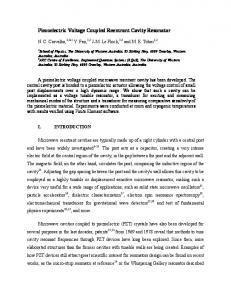
2. Model When considering a system consisting of two electrodes, one movable and one stationary, the situation can be depicted as in
Figure 2. (a) A schematic figure of the measurement problem and (b) simplified electrical equivalent for the system. φ1 and φ2 are the work functions of the electrode materials.
figure 2. To make the situation more generic we can assume that there is a layer of dielectric on the static electrode and the electrodes are fabricated from different materials with work functions φ1 and φ2 for static and movable electrodes, 5559
M Koskenvuori et al
respectively. The charges Q1 and Q2 on the electrodes can be written as Q1 = CV1
(3a)
Q2 = CV2 ,
(3b)
and where C is the total capacitance of the system. It should be noted that the voltages of the system appearing in the equations (bias-voltage, Udc and the work-function difference, φ12 ) are time independent and the only timedependent variable is the capacitance C1 . Keeping this in mind, equations (3a) and (3b) can be written as � � C1 (t)C2 Qox (Udc − φ12 ) − (4a) Q1 (t) = C1 (t) + C2 C2 and C1 (t)C2 C1 (t) + C2
Q2 (t) =
Udc = φ12 +
−(Udc − φ12 ) −
Qox , C1 (t)
(4b)
εA Cˆ 1 εA = = d + x(t) d + xvib sin(ωt) 1 + β sin(ωt) αC2 = , (5) 1 + β sin(ωt)
C1 (t) =
where ω is the angular frequency of the vibration and Cˆ 1 = εA/d is the capacitance at rest. α is defined as the ratio of the capacitances or α = Cˆ 1 /C2 and β is the relative amplitude of the vibration of the moving electrode, defined as β = xvib /d, where d is the initial distance between the moving and static electrodes and xvib is the amplitude of the vibration. Rewriting the equations (4a) and (4b) with the aid of the parameters α and β leads to αC2 (Udc − φ12 ) − αQox (1 + β sin(ωt)) + α
(6a)
Qox = Vbi , C2
(8)
where Vbi is the built-in voltage of the system. An approximate value for α can be calculated by writing α=
Cˆ 1 Aε0 Aε0 εr tox = = , / C2 d tox dεr
(9)
where tox and εr are the thickness and the dielectric constant of the dielectric on the static electrode, respectively. If we assume that the distance between the static and movable electrodes is in the order of d ≈ 5 µm and the dielectric on top of the static electrode is silicon dioxide (SiO2 ) having εr = 3.9, with thickness of 50 nm � tox � 200 nm, the value of α can be estimated to be 1/400 � α � 1/100. Within this film thickness range a 100 mV change in the built-in voltage requires an oxide charge in the range (1–4) × 1011 e cm−2 , which is over an order of magnitude smaller than that reported in oxide [4] and nitride [12] films. This indicates that the built-in voltage can be very susceptible to the charging of the dielectrics if the film thickness is increased. The value of β can be estimated from the limits set by the capacitive non-linearity. To minimize the generation of harmonic components the vibration amplitude should be only a few per cent of the gap [13]—from this the value of β can be estimated to be 1/100 � β � 1/20.
3. Set-up
and Q2 (t) =
(1 + β sin(ωt)Qox ) −αC2 (Udc − φ12 ) − . (6b) (1 + β sin(ωt)) + α (1 + β sin(ωt)) + α
The charge neutrality is maintained as Q1 + Q2 + Qox = 0. As the device is forced into vibration, the capacitance C1 changes and the charges on the electrodes are re-distributed. This re-distribution generates a current that can be measured when the circuit is closed with a set-up depicted in figure 3. As no additional charge is brought into the system and given that Qox is constant, the currents generated are equal and opposite dQ2 dQ1 =− dt dt −αβω cos(ωt)(C2 (Udc − φ12 ) − Qox ) = , ((1 + β sin(ωt)) + α)2
i(t) =
5560
for which i(t) = 0 when
�
�
where Qox is the charge on the dielectric layer, C1 is the capacitance over the air gap between the moving electrode and the surface of the dielectric and C2 is the capacitance over the dielectric on the static electrode. Udc is the applied dc voltage and φ12 is the contact potential due to the difference in the work functions of the movable and static electrode materials. Due to the forced vibration, C1 is time-dependent
Q1 (t) =
Figure 3. Circuit used to measure the current, i, generated by vibration of one of the micromechanical electrodes.
(7)
If the movable electrode is moving between two static electrodes as is the case in figure 3 the total force on the movable electrode is the sum of the forces on both sides of the electrode. If the built-in voltages on both sides are not equal, the capacitance over the air gap C1 is not constant throughout the Udc range. However, C1 can be assumed constant when |Udc | � |Vbi | or Ubias = Udc + Vbi ≈ Udc . Therefore the output is linear with higher values of Udc . In the set-up of figure 3 the bias-voltage is applied over both gaps simultaneously. This is necessary since besides being a necessity in the current generation, the applied voltage also exerts an attractive force between the electrodes and applying the voltage on one side only would tilt the moving electrode and change the separation between the electrodes leading to a change in the parameter α. This in turn would
Built-in voltage inside closed cavity MEMS-devices 1.5 Symmetric biasing Single-sided biasing
Output voltage [mV]
Output voltage [arb.units]
1 0.5 0 y = 1.197x + 0.0814
-0.5
Vbi = -b/a Vbi = 0.0814/1.197 V Vbi = -68 mV
-1 -2.5
-2
-1.5
-1
-0.5
0
0.5
1
1.5
2
2.5
Applied DC-voltage [V]
-1.5 -1
Figure 4. Simulated results when the biasing is symmetric (constant α) and un symmetric (variable α).
-0.8
-0.6
-0.4
-0.2
0
0.2
0.4
0.6
0.8
1
Applied voltage [V]
Figure 6. Measurement result and a linear fit to the data.
DUT
In
Lock-in amplifier RefOut Shake
± Out
Power amplifier
In Out
Voltage sources
DCbias
In
Multimeter
Figure 5. Schematic of the measurement set-up. The vibration on the DUT is generated with a mechanical shaker that is driven with amplified signal from lock-in amplifier at the frequency ω. The current is transformed to a voltage with a circuit in figure 3 and the voltage is recorded as a function of the bias-voltage. The bias voltage is generated with two voltage sources to provide both positive and negative polarities. All the instruments are connected to the computer with GPIB.
lead to C1 not being constant over the bias-voltage sweep. The minimum position of the current would not be changed, but the fitting of the curve to the measured data would become more difficult. This is easily seen from figure 4. With a set-up shown in figure 5 the movable electrode inside the device under test (DUT) is forced to vibrate at a frequency ω with a mechanical shaker. The generated current at the vibration frequency ω is transformed into a voltage with an operational amplifier (figure 3) and detected with a lock-in amplifier. From (7) it can be seen that the sensitivity of the system increases with increased frequency, but to ensure the proper operation the excitation frequency should be kept below any resonant frequencies of the DUT. The output is a straight line as a function of the applied dc voltage, Udc (figure 6). As α � 1 and β � 1 in (7) this linear behaviour can also be seen by writing the approximation of (7) as i(t) ≈ −αβω cos(ωt)(C2 (Udc − φ12 ) − Qox ) × ((1 − (β sin(ωt)) + α))2
(10)
and collecting the terms with ω dependence. By fitting a line to the data points, the built-in voltage can be deduced very easily. The vibration is generated by a Bruel&Kjaer type 4810 minishaker which is driven by the lock-in amplifier (Stanford Research Systems SR830) through a power amplifier (HP 6825A) at the frequency ω. The bias voltage is generated by series connected voltage sources (Agilent 6614C) in order to
Figure 7. Cross-section of the measured accelerometer. The static electrodes have AlCu metallization with SiO2 layer covering the metallization. (This figure is in colour only in the electronic version) Table 1. Electrode materials Sample
Static electrode
Moving electrode (Proof mass)
1–4 5–9 10–12 13–15 16–19
Mo AlCu AlCu + 50 nm SiO2 AlCu + 200 nm SiO2 Ta
Mo Si Si Si Ta
produce both negative and positive bias-voltages. In order to maximize the accuracy, the bias voltage is measured with the multimeter (Agilent 3458A) at the same time it is connected to the vibrating capacitor. In principle, the vibration can also be achieved by applying an ac-voltage (U = u sin(ωt)) to the vibrating capacitor. Then the force exerted on the proof mass can be written as F = −∇E =
1 ∂C 2 U , 2 ∂x
1 ∂C 2 u (1 + cos(2ωt)), 4 ∂x 1 C0 2 u (1 + cos(2ωt)), ≈ 4 d =
(11)
5561
M Koskenvuori et al Applied voltage [V] -2.5
-2
-1.5
-1
-0.5
0
0.5
1
1.5
2
2.5
1.5
8.4
8.35
0.5
8.3
0
8.25
-0.5
Capacitance [pF]
Output voltage [mV]
1
8.2 Kelvin - gap 1 Kelvin - gap 2 CV - gap 1 CV - gap 2
-1
8.15
-1.5
8.1 -1
-0.75
-0.5
-0.25
0 0.25 Applied voltage [V]
0.5
0.75
1
Figure 8. Figure showing the measurement of both gaps with both the methods. The measurement corresponds to sample number 9 in figure 9.
4. Samples and measurement results To test the method 19 accelerometers were measured. The devices were fabricated by anodically bonding three wafers: a silicon wafer with proof-mass in between two glass covered silicon wafers supporting the static electrodes (figure 7). The static electrodes were metal with a dielectric layer on top in some samples. The proof-mass was either silicon or silicon metallized with molybdenum or tantalum (table 1). The silicon is boron doped (NA = 2 × 1019 cm−3 ) with additional boron doping on the surface of the proof mass (NA = 4×1019 cm−3 ). The electrode area A = 1.45×10⁻⁶ m2 , the air gap d = 5.7 µm and spring constant k = 30 N m−1 for all the samples. As a result of the anodic bonding the pressure inside the cavity is enough to over-damp the resonance of the proof-mass. To ensure the desired motion of the proof-mass the mechanical excitation was done below the resonance frequency of the proof-mass and for this purpose the excitation frequency of ω = 2π × 60 Hz was selected. Both gaps of the accelerometer were measured with both the C–V method and the proposed method (vibrating capacitor or Kelvin method). A result of a measurement is shown in figure 8. The actual built-in voltages are deduced by fitting a parabola to C–V measurements and a line to measurements with the proposed method. 5562
100 50
CV - gap 1 CV - gap 2 Kelvin - gap 1 Kelvin - gap 2
0
Vbi [mV]
where C0 is the capacitance at rest, C0 = εA/d where A is the area of the capacitance and ε is the permittivity of the medium between the electrodes. The last approximation in (11) holds when the vibration amplitude, x, is small when compared with the electrode separation at rest, d. From (11) the problems of electrostatic excitation are evident: (i) The weak force exerted will be at the double frequency when compared with the excitation voltage and (ii) the force is dependent on the distance, d, between the movable and static electrodes. The actuation force can be increased by increasing the voltage, but increased voltage can lead to increased trapping of the charges and change the actual builtin voltage [14, 15].
-50 -100 -150 -200 -250 1
2
3
4
5
6
7
8
9 10 11 12 13 14 15 16 17 18 19 Sample #
Figure 9. Comparison of the measured built-in voltages. The surrounding boxes indicate a group of similar accelerometers whose properties are explained in table 1. It is clear that the results gained with the C–V measurements (� and �) and the results gained with the proposed method (× and +) agree well.
The extracted built-in voltages from the 19 accelerometers are collected in figure 9. The results indicate that both the measurements give similar results even though the builtin voltages vary a lot from device to device. Thorough analyses of the reasons for these device to device variations and variations from the theoretical values of the built-in voltages are outside the scope of this paper. As a further point, it should be noted that the results are consistent and qualitatively identical between the two presented methods even if the builtin voltage is significantly altered by, for example, a dielectric layer indicating that both the methods measure the same property. The root mean square of the difference between the methods is 14.25 mV, which can be explained by the different measurement conditions—the different measurements were performed with different measurement sets and the samples were moved from one set-up to another by hand which is enough to cause a slight discrepancy between the measurement conditions. Previous measurements relied on measuring 41 points with the proposed method. As the behaviour is highly linear, this many measurements are not really needed. To probe the
Built-in voltage inside closed cavity MEMS-devices 0.25
0.2
0.08
1
2
0.5 0 -0.5 -1 -1.5 -1.25
0.1
-0.75
-0.25
0.25
0.75
Applied voltage [V]
1.25
1.5 1
0.06
0.5 0 -0.5 -1 -1.5 -1.25
-0.75
-0.25
0.25
0.75
1.25
0.04
Error [mV]
0.15
1.5 Output voltage [mV]
Output voltage [mV ]
2
Error [%]
Acknowledgments
0.1
The financial support from the Finnish National Technology Agency TEKES, VTI Technologies and Vaisala is acknowledged. M Koskenvuori thanks Jenny and Antti Wihuri Foundation, the Finnish Academy of Science and Letters and Vilho, Yrj¨o and Kalle V¨ais¨al¨a Foundation for scholarships.
Applied voltage [V]
0.05
0.02
References 0
0 0
5
10
15
20 25 # of data points
30
35
40
Figure 10. Error in the Vbi when the number of measurement points is reduced. The example corresponds to the gap 1 of sample number 13 in figure 9. The number of points from the right to the left are [41,10,4,2].
limits of the measurement, a built-in voltage was deduced from the measured data (in figure 8) with the number of points reduced to 10, 4 and 2 (the data are removed from the middle of the measurement, i.e. the results for the highest absolute bias-voltage values are kept and a linear fit for the remaining points is performed (see insets of figure 10)). This calculated value of Vbix (x = [10, 4, 2]) is compared with the original value received by measuring 41 points (Vbi41 ) and the errors |Vbi41 − Vbix |/Vbi41 and |Vbi41 − Vbix | are plotted in figure 10. It can easily be seen from figure 10 that when the Kelvinmeasurement is done only at two points, the error is less than 0.25%. It can be translated as an error in the built-in voltage as �Vbi ≈ 0.6 mV for even the samples with the highest absolute values of Vbi (sample number 3). This indicates that as long as the bias-voltages are selected so that |Udc | � |Vbi | this measurement method gives very accurate results by measuring the output current with just two values of the bias-voltage making the measurement very fast and convenient.
5. Conclusions A method to measure the built-in voltages, Vbi , of micromechanical devices is presented and compared with an existing method with a good qualitative match. The presented method is based on a vibrating capacitor (Kelvinprobe) method where the capacitance is biased with a dc voltage, Udc and the generated current is measured. It is shown that if the biasing voltage Udc � Vbi the measurement can be performed by measuring only a few data points without compromising the accuracy.
[1] Bannon F D, Clark J R and Nguyen C T-C 2000 High-Q microelectromechanical filters IEEE J. Solid State Circuits 35 512–26 [2] Lee S, Demirci M U and Nguyen C T-C 2001 A 10 MHz micromechanical resonator pierce reference oscillator for communications Tech. Dig. Transducers ’01, 11th Int. Conf. on Solid-State Sensors and Actuators (Munich, Germany, 10–14 June 2001) pp 1094–7 [3] K¨arkk¨ainen A 2006 MEMS based voltage references Doctoral dissertation (Espoo: VTT Publications) [4] Wibbeler J, Pfeifer G and Hietschold M 1998 Parasitic charging of dielectric surfaces in capacitive microelectromechanical systems (MEMS) Sensors Actuators A 71 74–80 [5] Ashcroft N W and Mermin N D 1976 Solid State Physics (Philadelphia, PA: Holt, Rinehart and Winston) [6] Sze S M 2002 Semiconductor Devices 2nd edn (New York: Wiley) [7] M¨onch W 1995 Semiconductor Surfaces and Interfaces (Berlin: Springer) [8] Durakiewicz T, Arko A, Joyce J J, Moore D P and Halas S 2001 Thermal work function shifts for polycrystalline metal surfaces Surf. Sci. 478 72 [9] L¨uth H 1998 Surfaces and Interfaces of Solid Materials (Berlin: Springer) [10] Lord Kelvin 1898 Contact electricity on metals Phil. Mag. 46 82 [11] Schroder D K 2002 Contactless surface charge semiconductor characterization Mater. Sci. Eng. B 91–92 196–210 [12] Tang W C, Lim M G and Howe R T 1992 Electrostatic comb drive levitation and control method J. Microelectromech. Syst. 1 170–8 [13] Kaajakari V, Mattila T, Oja A and Sepp¨a H 2004 Nonlinear limits for single-crystal silicon microresonators J. Microelectromech. Syst. 13 715–24 [14] Goldsmith C L, Ehmke J, Malczewski A, Pillans B, Eshelman S, Yao Z, Brank J and Eberly M 2001 Lifetime characterization of capacitive RF MEMS switches Tech. Dig. IEEE MTT-S Int. Microwave Symp. (Phoenix, AZ, USA, 20–25, May 2001) pp 227–30 [15] Merlijin van Sprengen W, Puers R, Mertens R and de Wolf I 2004 A comprehensive model to predict the charging and reliability of capacitive RF MEMS switches J. Micromech. Microeng. 14 514–21
5563