Dec 30, 2014 - PHYSICAL REVIEW B 90, 245311 (2014) ... 1Department of Physics, University of Michigan, 450 Church Street, Ann Arbor, Michigan 48109, ...
PHYSICAL REVIEW B 90, 245311 (2014)
Carrier dynamics in site- and structure-controlled InGaN/GaN quantum dots Lei Zhang,1 Tyler A. Hill,1 Chu-Hsiang Teng,2 Brandon Demory,2 Pei-Cheng Ku,2 and Hui Deng1 1
2
Department of Physics, University of Michigan, 450 Church Street, Ann Arbor, Michigan 48109, USA Department of Electrical Engineering and Computer Science, University of Michigan, 1301 Beal Avenue, Ann Arbor, Michigan 48109, USA (Received 6 May 2014; revised manuscript received 3 November 2014; published 30 December 2014) We report on the carrier dynamics in InGaN/GaN dot-in-nanowire quantum dots, revealed by a systematic mapping between the optical properties and structural parameters of the quantum dots. Such a study is made possible by using quantum dots with precisely controlled locations and sizes. We show that the carrier dynamics is governed by two competing mechanisms: (1) Excitons are protected from surface recombination by a potential barrier formed due to strain relaxation at the sidewall surface. (2) Excitons can overcome the potential barrier by tunneling and thermal activation. This carrier dynamics model successfully explains the following surprising experimental findings on individual quantum dots. First, there exist strong statistical correlations among multiple optical properties of many individual quantum dots, despite variations of these properties resulting from inevitable structural variations among the quantum dots. Second, the antibunching property of the quantum dot emission exhibits an abnormal ladle-shaped dependence on the decay time and temperature. Our results can guide the way toward nitride-based high-temperature single-photon emitters and nanophotonic devices. DOI: 10.1103/PhysRevB.90.245311
PACS number(s): 78.67.Hc, 78.55.Cr, 78.47.jd, 73.21.La
I. INTRODUCTION
Nitride-based quantum dots (QDs) are one of the most promising candidates for achieving on-chip, scalable, electrically driven single-photon sources at the room temperature [1–3]. The optical performance of these devices, such as their quantum efficiency (QE), operation speed, and single-photon purity, critically depends on the carrier dynamics, such as the radiative and nonradiative decay rates of the carriers. The carrier dynamics, in turn, is determined by nanoscale structural parameters, such as the diameter, thickness, material composition, and surface properties of the QD. Therefore, the key to improve the performance is to know what the structural parameters are and how they impact the performance. However, it is nearly impossible to directly measure all the relevant structural parameters of every single QD nondestructively with sufficient accuracy using current technologies [4]. Furthermore, correlations between the optical properties and the structural parameters were obscure in previous studies in which the QDs were typically formed at random positions with large structural inhomogeneities [5,6]. Alternatively, we have recently demonstrated high-quality site-controlled InGaN QDs in GaN nanowires, whose structural parameters were controlled to the limit of the state-ofthe-art growth and nanofabrication technologies [7,8]. Using these QDs, we are able to systematically study the optical properties of QDs with diameters ranging from 19 to 33 nm, using time-integrated photoluminescence (PL) spectroscopy, time-resolved PL (TRPL), and the second-order correlation (g (2) ) measurements, at temperatures from 10 to 120 K. Such a study allows us to observe strong correlations between the structural parameters and optical properties and, based on which, extract the underlying carrier dynamics in these nitride-based QDs. In addition, we show that, opposed to the common practice of assuming 100% quantum efficiency at low temperatures in dot in nanowires, quantum tunneling leads to significant surface recombination in some QDs even at temperatures down to 10 K. Furthermore, contrary to conventional expectations, 1098-0121/2014/90(24)/245311(13)
we show that the best photon antibunching does not always occur in the brightest QDs or at the lowest temperatures for our QDs. The above observations are intuitively explained by our carrier dynamics model, providing guidance for future improvement of single-photon sources based on III-nitride QDs. This paper is organized as follows. Section II presents the QD sample structure and the optical setup used to study it. Section III presents the principles of the carrier dynamics and explains its strong dependence on structural parameters and, therefore, the necessity of using site- and structure-controlled QDs to study it. In Secs. IV and V, we establish the main control mechanisms and parameters of carrier dynamics, using QD ensembles of different diameters. In Sec. IV, we identify a lateral confinement potential for the excitons and extract its analytical form based on the diameter dependence of the PL energy of the QDs. In Sec. V, we extract the key parameters needed to model the radiative, tunneling, and thermal decay rates of excitons in our QDs, based on the diameter and temperature dependencies of the PL decay time of the QDs. In Secs. VI and VII, we extend the carrier dynamics model to describe properties of individual QDs. In Sec. VI, we identify the sources of inhomogeneities in the PL properties among individual QDs of closely matched structural parameters, and we explain the statistical correlations among these PL properties using the carrier dynamics model. Section VII includes the biexciton dynamics into the model by considering exciton-exciton interactions and explains the peculiar decay time and temperature dependence of the degree of photon antibunching. Finally, we summarize the main findings in Sec. VIII. II. SAMPLE STRUCTURE AND OPTICAL SETUP
The QDs studied in this work were fabricated via electronbeam patterning and plasma etching a planar single InGaN/GaN quantum well (QW) [9]. Details of the fabrication process can be found in [8,9]. Each individual QD was made of a 3-nm-thick In0.15 Ga0.85 N nanodisk in a 120-nm-tall GaN
245311-1
©2014 American Physical Society
ZHANG, HILL, TENG, DEMORY, KU, AND DENG
PHYSICAL REVIEW B 90, 245311 (2014)
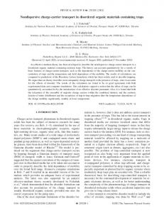
longer than 400 nm through. For the TRPL measurements, an additional pair of tunable bandpass filters (Semrock TBP01449/15) was used to select a spectral window whose position was tunable from 400 to 440 nm and bandwidth was tunable from 2 to 10 nm. A CCD camera was used to monitor the position of the QDs through their PL. The PL spectrum was measured using a spectrometer [part of the PL/TRPL box in Fig. 1(c)] with a 0.6-meV (0.08-nm) spectral resolution at ∼3 eV (400 nm). The second-order correlation (g (2) ) function of single QDs was measured using a Hanbury-Brown-Twiss (HBT) interferometer [10] composed of a 50:50 unpolarized beam splitter, two avalanche photodetectors (APDs), and a time correlator (TC). One of the APD-TC arms was also used for the TRPL measurement (not shown in Fig. 1) with a synchronization signal from the Ti:sapphire laser. The APD-TC system’s instrument response function (IRF) at 400 nm had a ∼0.2-ns full width at half-maximum (FWHM), which corresponds to the time resolution of the TRPL and g (2) measurements. FIG. 1. (Color online) (a) The schematic of a single GaN nanopillar containing an InGaN nanodisk of a diameter D = 25 nm. (b) The scanning electron microscope image of a part of a dense array of QDs of a diameter D = 25 nm and dot-to-dot separation 300 nm. The viewing angle is 45◦ . (c) The schematic of the optical setup used in this work, in which SHG stands for second harmonic generation; CCD, charge-coupled device; PL/TRPL, photoluminescence and timeresolved photoluminescence measurement setup; APD, avalanche photodiode; and TC, time correlator.
nanopillar, as illustrated in Fig. 1(a). The nanodisk had a 10-nm-thick GaN at the top and had sidewalls exposed in air. We studied multiple dense and sparse arrays of QDs with diameters ranging from 19 to 32 nm. Each dense array consisted of 100 × 100 QDs with a 300-nm interdot separation [Fig. 1(b)] for measurements of QD ensembles. Each sparse array (not shown) consisted of 10 × 10 QDs with a 5-μm interdot separation for measurements of individual QDs. The diameters of all InGaN QDs in the same array were nominally the same with ∼2-nm standard deviation. On the same sample we also have micropillars whose structures are similar to the nanopillars in Fig. 1(a) except that their InGaN microdisks are 5 μm in diameter. These microdisks exhibit QW properties [14] and are referred to as QW microdisks in this work. The optical setup used in this work is illustrated in Fig. 1(c). The sample was placed in a temperature-stabilized He-flow cryostat. It was excited from an angle of 55◦ from the normal direction with a 390-nm laser obtained by frequency doubling a 780-nm Ti:sapphire laser. The laser had a pulse duration of 150 fs and a repetition rate of 80 MHz. The laser spot on the sample surface was elliptical, with a short axis of 20 μm and a long axis of 35 μm. We studied the PL and TRPL of QDs using a confocal microscope setup composed of an objective lens (L1, f = 5 mm, 0.6 NA) and a pair of confocal lenses (L2 and L3, f = 75 mm). The setup was switchable between measuring an ensemble of QDs and a single-QD by removing or placing a 25-μm pinhole at the confocal plane. The pinhole was capable of isolating the emission of a single QD in a sparse array. A longpass filter (Semrock FF02-409/LP) was used to remove the scattered laser and only allow wavelengths
III. PRINCIPLES OF THE CARRIER DYNAMICS
In this section, we summarize the principles of the carrier dynamics and how they were identified using our site- and structure-controlled QDs. The detailed deduction of the model based on the experimental data will be presented in later sections. In our QDs, the nonradiative decay is determined by two competing processes: on one hand, the strain relaxation at the sidewall forms a confinement potential protecting excitons from recombining with the nonradiative surface states; on the other hand, excitons can overcome the potential barrier through tunneling and thermal activation. In an etched InGaN/GaN nanodisk, the lateral confinement potential for the exciton is formed due to strain relaxation at the sidewall [11–13], as illustrated in Fig. 2(a). This is manifested as a continuous blue-shift of the QD PL energy with the reduction of the diameter (Fig. 4), which shows the piezoelectric field is the determining factor of the potential profile, as explained in [14]. The larger strain relaxation at
FIG. 2. (Color online) (a) Exciton decay model. A lateral potential profile is formed mainly due to the reduction in the piezoelectric field at the nanodisk sidewall. An exciton decays mainly through three channels: the radiative decay and the tunneling and thermal surface nonradiative decay, whose decay rates are denoted as γr , γtnl , and γthm , respectively. The latter two processes need to overcome the lateral potential barrier. (b) Biexciton decay model. The presence of another exciton lowers the potential barrier experienced by any of the two excitons due to the screening effect, leading to a lower biexciton QE compared to exciton QE.
245311-2
CARRIER DYNAMICS IN SITE- AND STRUCTURE- . . .
PHYSICAL REVIEW B 90, 245311 (2014)
the sidewall compared to the center of the nanodisk leads to a weaker piezoelectric field and, thus, higher exciton energy. The resulting confinement potential protects excitons from reaching the detrimental sidewall surface, and thus plays a critical role in exciton dynamics. The potential profile will be obtained in Sec. IV. The exciton dynamics is governed by its radiative and nonradiative mechanisms. We will examine them in Sec. V by the diameter and temperature dependence of the PL intensity and decay time of QD ensembles. Here, we first present the main principles of the radiative and nonradiative decay. The radiative decay rate γr of an exciton in an InGaN/GaN nanodisk is determined by its oscillator strength, the local density of photon states (LDPS), and the temperature. The oscillator strength increases due to strain relaxation, whereas the LDPS decreases as the nanodisk diameter is reduced [14]. Meanwhile, since an exciton can be thermally scattered out of the radiation zone in the momentum space, the averaged γr is expected to decrease as the temperature increases [15,16]. The relative γr is reflected by the ratio of the PL intensity and the decay time, as will be explained in Sec. V A. The nonradiative decay of an exciton can occur both at the surface and in the volume of a QD. The volume recombination includes the Shockley-Read-Hall [17,18] and Auger [19] processes. In our QDs, the volume recombination was negligible because, at any given temperature, the measured total decay time of the planar QW on the same sample was over 10 times longer than that of the QDs [14]. The surface nonradiative recombination is a major concern for nanostructures with large surface-to-volume ratios. There are two types of surface nonradiative decay processes, based on the way excitons overcome the potential barrier and reach the sidewall surface: the tunneling decay and thermal decay, as illustrated in Fig. 2(a), which are analogous to the field emission and thermionic emission in the standard Schottky barrier theory [20,21]. The tunneling decay is the dominant nonradiative decay mechanism at low temperatures in our QDs. It is due to the tunneling of the exciton through the potential barrier to the surface, and is determined by the wave-function overlap of the exciton and surface states. Hence, the tunneling decay rate γtnl is finite even at zero temperature as shown in Sec. V B. It strongly depends on the potential barrier profile and only weakly depends on the temperature, similar to the thermionicfield-emission component in the Schottky barrier theory [20]. The thermal decay becomes the dominant nonradiative decay mechanism as the temperature increases. It is due to the thermal activation of the exciton over the potential barrier to the surface. Therefore, the thermal decay rate γthm depends strongly on the temperature as well as the potential barrier profile as shown in Sec. V C. Experimentally characterizing the radiative, tunneling, and thermal decay independently is, however, far from straightforward since only the total decay rate and PL intensity can be directly measured. Each of these decay rates varies differently with the potential profile, while the potential profile is determined by multiple structural parameters of the QD, such as the diameter, thickness, and indium mole fraction. Therefore, to obtain the dependence of each decay mechanism on each structural parameter, one would have to
measure the change of the optical properties while varying each structural parameter separately. This cannot be done with QDs self-assembled at random sites, whose structural parameters are often correlated with each other and suffer from large inhomogeneity. On the other hand, using the site- and structure-controlled QDs described in Sec. II, we can measure the dependence of the optical properties on one of the structure parameters while keeping the fluctuations in others minimal. This enables us to extract the decay rates and their dependence on various structural parameters, as we discuss in Sec. V. Despite our control of the structural parameters, small fluctuations in these parameters are inevitable. This leads to inhomogeneities in the optical properties of QDs with the same nominal structural parameters, as shown in Sec. VI A. However, with the tight control of the structural parameters, it turns out that the inhomogeneities in all measured optical properties are strongly correlated with each other, as shown in Sec. VI B. As a result, variations in different optical properties can all be modeled by the variation of one parameter, which is identified as the height of the sidewall potential barrier. The above carrier dynamics model describes well the intensity and decay time of the QD emission, which is dominated by emission from the exciton state at the lowexcitation power densities used in this work. However, to describe the photon-antibunching property of QDs when the exciton and biexciton emission overlap spectrally overlap [22–25], biexciton dynamics needs to be included. The biexciton emission is different from the exciton emission due to the biexciton binding energy. The biexciton binding energy can be extracted from the overall spectral linewidth, as explained in Sec. VII A. It is typically negative in InGaN QDs, due to the repulsive electron-electron (hole-hole) Coulomb interaction between the two electron-hole pairs (EHPs) in a biexciton [14,26–30]. As a result, the sidewall potential barrier is lower for the biexciton than for the exciton by the biexciton binding energy. This allows us to explain the peculiar correlation between the photon antibunching and other PL properties in Sec. VII C and the abnormal temperature dependence of the photon antibunching in Sec. VII D. IV. LATERAL POTENTIAL BARRIER PROFILE
As explained in the preceding section, the carrier dynamics in an InGaN/GaN nanodisk strongly depends on the exciton potential profile in the nanodisk. Therefore, the first step towards modeling the carrier dynamics is to identify the sources of the potential. There are several mechanisms that could lead to an inplane potential for the excitons in the InGaN/GaN nanodisk, including the nonuniform distributions of the deformation potential and the spontaneous and piezoelectric polarizations due to the uneven strain distribution from the center to the sidewall of the nanodisk [13,31]. Note that we do not consider the contribution of the surface Fermi-level pinning [6,32] because it bends the conduction and valence bands in the same way and thus has negligible effects on the in-plane potential for the exciton. To identify the main source of the potential, we examine the diameter dependence of the exciton energy, following the
245311-3
ZHANG, HILL, TENG, DEMORY, KU, AND DENG
PHYSICAL REVIEW B 90, 245311 (2014)
FIG. 4. (Color online) (a) The PL energy E vs the QD diameter D of nine dense arrays of QDs with diameters ranging from 19 to 33 nm and a 5-μm-diameter QW microdisk taken at the excitation power density P = 1 W/cm2 . The inset is a zoomed-in version of the nine dense QD arrays. The solid line is a fitting curve based on Eq. (2). The axes of the inset have the same units as the main figure. (b) The exciton potential profiles of QDs of diameters D = 19, 22, 25, 29, 33, and 600 nm, calculated using Eq. (1). The inset is a zoomed-in version of the five smaller diameters. The axes of the inset have the same units as the main figure. FIG. 3. (Color online) QD ensemble PL and TRPL taken at the excitation power density P = 1 W/cm2 . (a) The PL spectra of ensembles of QDs of diameters D = 21, 25, and 29 nm and a QW of a diameter of 5 μm at 10 K. The PL intensity is normalized by the area of the InGaN layer. The spectrum of the QW is multiplied by a factor of 8 for better visibility. (b) The TRPL of ensembles of QDs of diameters D = 21, 25, and 29 nm at 10 K. (c), (d) The PL spectra and TRPL of an ensemble of QDs of diameter D = 29 nm at temperature T = 10, 50, and 80 K.
same procedure as in [14]. We measure the PL spectra of nine dense arrays of QDs with diameters varying from 19 to 33 nm as well as a QW microdisk with a diameter of 5 μm, all on the same sample, at 10-K temperature. We use a very low-excitation power density of P = 1 W/cm2 to avoid significant screening of the electric field. Figure 3(a) shows the PL spectra of the QW microdisk and several QDs. Each spectrum is composed of a dominant zero-phonon band (ZPB) and a serial of optical-phonon (OP) replicas at the lower-energy side of the ZPB. The OP replicas of the QW microdisk are more pronounced compared to those of QDs due to the strain-enhanced wave-function overlap between carriers and the longitudinal interface OP modes [33,34]. The PL intensity of the QW microdisk is weaker compared to those of QDs due to the suppression of the exciton oscillator strength in the QW microdisk [14,35–39]. Note that PL intensity in this study is normalized to the area of the InGaN layer and corrected by the collection and absorption efficiencies calculated by finite-difference time-domain (FDTD) simulations [14]. Figures 3(a) and 4(a) show that the peak energy of ZPB blue-shifts as the diameter of the QD reduces from 5 μm to 19 nm, consistent with previous studies [14,35–41]. The large amount of blue-shift (∼500 meV) from QW to QD shows that the piezoelectric polarization gives the dominant contribution to the exciton potential profile in our QDs [14]. The piezoelectric polarization lowers the exciton energy due to the quantum-confined Stark effect [42]. Therefore, reducing the diameter decreases the overall strain and piezoelectric polarization, leading to an increase in the exciton energy. In contrast, the deformation potential increases the band
gap [31] and would lead to a red-shift of the exciton energy with decreasing nanodisk diameter. The spontaneous polarization also cannot explain the blue-shift since it is largely independent of the strain and, therefore, the nanodisk diameter. The predominance of the piezoelectric polarization in shaping the potential profile suggests a lower exciton potential at the center of the nanodisk, as illustrated in Fig. 2(a). This is because the higher residue strain at the center of the nanodisk leads to a stronger piezoelectric field and Stark red-shift compared to at the sidewall. Following the phenomenological model in [14], the resulting potential profile at the radial position r can be described as φ � (r) = −Bm [1 − sech(κD/2) cosh(κr)].
(1)
Here, Bm represents the amount of exciton energy shift from an unstrained QW to a fully strained QW, 1/κ is the characteristic length of the region from the InGaN nanodisk sidewall where the compressive strain of the InGaN layer is relaxed, and D is the nanodisk’s lateral diameter. Due to the predominance of the piezoelectric polarization over the deformation potential, Bm is always positive, i.e., φ � (0) < φ � (D/2). At low-excitation power densities, the diameter-dependent PL energy E(D), corresponding to the exciton energy at r = 0, can be written as E = E0 − Bm [1 − sech(κD/2)].
(2)
Here, E0 is the exciton energy at r = D/2 where the strain is considered as being fully relaxed. Therefore, it represents the band gap of an unstrained QW or a nanodisk of D → 0. The characteristic strain relaxation parameters Bm and κ as well as E0 are obtained by using Eq. (2) to fit the measured E(D) data, as shown in Fig. 4(a). We obtain, for this particular sample, E0 = 2.93 eV, Bm = 477 meV, and 1/κ = 27 nm. With Bm and κ, we can use Eq. (1) to calculate the exciton potential profile for QDs with different diameters, as shown in Fig. 4(b). For describing the carrier dynamics, only the shape of the potential profile matters. For convenience in later discussions,
245311-4
CARRIER DYNAMICS IN SITE- AND STRUCTURE- . . .
PHYSICAL REVIEW B 90, 245311 (2014)
we shift the φ � (r) in Eq. (1) by an r-independent constant to obtain φ(r) so that φ(r = 0) = 0: φ(r) = Bm sech(κD/2)[cosh(κr) − 1].
(3)
For a QD of diameter D, φ(r) reaches the maximum and minimum at r = D/2 and 0, respectively, i.e., the potential barrier height is φB = φ(D/2) − φ(0) = Bm [1 − sech(κD/2)].
(4)
V. DECAY RATES
As explained in Sec. III, an exciton in a QD mainly undergoes three decay processes: the radiative, tunneling, and thermal decay [Fig. 2(a)]. In this section, we show that, to consistently explain all measured diameter and temperature dependence of the total decay time and PL intensity in this study, the total decay rate γ = γr + γtnl + γthm has to be expressed as γ = γr0 (1 − e−�/kB T ) + +
c2 vB −c3 φB /kB T e . D
c1 − 2√2m � D/2 √φ(r)dr e � 0 D (5)
The three terms on the right-hand side correspond to γr , γtnl , and γthm , respectively. We will show in Sec. V A, in the γr term, γr0 is the radiative decay rate at temperature T → 0, it is independent of the QD diameter D for 21 nm < D < 33 nm; kB is the Boltzmann constant; and � is the exciton’s homogeneous linewidth, limited mainly by impurities and interface scattering. γr decreases as T increases, due to the thermal scattering of the excitons out of the radiation zone [15]. We will show in Sec. V B, in the γtnl term, c1 /4 is the surface recombination velocity of unstrained InGaN at zero temperature; m is the exciton effective mass; and√ � �is the reduced Planck constant. D/2 √ − 2 �2m 0 φ(r)dr The exponential factor e is proportional to the probability for a ground-state exciton to tunnel through the potential profile φ(r) to the sidewall surface; the 1/D factor takes into account the surface-to-volume ratio. We will show in Sec. V C, in the γthm term, c2 vB /4 is the thermally induced surface recombination velocity for unstrained InGaN; c3 is a factor that adjusts the potential barrier height to account for the temperature-dependent part of the tunneling decay; the exponential factor e−c3 φB /kB T is the thermal population of the excitons with √ kinetic energies higher than c3 φB ; vB is defined as vB = 2(c3 φB + kB T )/m, the average velocity of the excitons with kinetic energies higher than c3 φB . The parameters φ(r) and φB in Eq. (5) have been obtained in Sec. IV. The remaining five unknown parameters in Eq. (5), γr0 , �, c1 , c2 , and c3 , can be obtained from carefully designed control experiments. These include measuring the diameter and temperature dependence of the PL intensity I and the total decay time τ = 1/γ of QD arrays with tightly controlled structural parameters, as shown in Figs. 3 and 5. The diameter and temperature dependence of γr can be obtained from the ratio of the PL intensity and the total decay time I /τ . At low temperatures, τr is approximately τr0 , and we found it to be independent of QD diameter D as shown in Fig. 6(a). Since at T → 0, γthm is negligible, the total decay
FIG. 5. (Color online) (a) The total decay time τ (square, left axis) and PL intensity I (triangle, right axis) vs QD diameter D of dense arrays at 10 K. The τ (D) data are fitted using Eq. (6), yielding γr0 = 59 MHz and c1 = 15 m/s. (b) The I (T ) data of four dense arrays with QD diameters D = 22 nm (square), 25 nm (circle), 29 nm (triangle), 33 nm (star) nm, respectively. (c) The τ (T ) data of the same four arrays described in (b), which are simultaneously fitted using Eq. (5), yielding c2 = 2 × 10⁻³ and c3 = 0.33, as shown by the solid, dashed, thick dashed, and thick solid curves. The fitting takes into account the instrument time resolution of 0.2 ns (Sec. II).
rate in Eq. (5) can be simplified into γ (D,T → 0) = γr0 + γtnl = γr0 +
c1 − 2√2m � D/2 √φ(r)dr e � 0 . D (6)
From the τ (D,T → 0) data in Fig. 5(a), we obtained γr0 and c1 . � is obtained from the τr (T ) data in Fig. 6(b), which are generated from Figs. 5(b) and 5(c) using Eq. (7). Finally, after
FIG. 6. (Color online) (a) The relative τr (D) extracted from the I (D) and τ (D) data in Fig. 5(a) using Eq. (7). τr (D) is normalized to the average value (dashed line). (b) The τr (T ) relation of dense arrays with D = 22 nm (blue square), 25 nm (red circle), 29 nm (green triangle), 33 nm (cyan star) nm. Each τr data point is proportional to the ratio of the corresponding τ and I values in Figs. 5(c) and 5(b), respectively. All four sets of the data are then fitted together using Eq. (8) with γr0 and � being the fitting parameters, resulting in � = 8.6 meV and a γr0 value. All the data and the fitted curve (solid line) are scaled in the way such that γr0 = 59 MHz, as obtained in Fig. 5(a).
245311-5
ZHANG, HILL, TENG, DEMORY, KU, AND DENG
PHYSICAL REVIEW B 90, 245311 (2014)
obtaining all the parameters related to γr and γtnl , we obtain the γthm parameters, c2 and c3 , by fitting the τ (T ) data in Fig. 5(c) using Eq. (5). In the rest of this section, we will provide further explanations for the expression of each decay channel in Eq. (5) and the procedures for extracting the five parameters from Figs. 5 and 6. A. Radiative decay rate
First, we show that the radiative decay rate γr of our QDs is mostly independent of the QD diameter D at 21 nm < D < 33 nm. γr can be calculated from the total decay rate γ and the PL intensity I [43] using the following equation: γr ∝ γ I.
(7)
This is because, on one hand, γr of an exciton is related to the total decay rate γ and QE η via η = γr /γ = γr /(γr + γnr ), in which γnr is the nonradiative decay rate; on the other hand, η is proportional to I , for QDs of diameter 10 nm < D < 40 nm excited by the same laser intensity [14]. Applying Eq. (7) to the τ (D) (τ = 1/γ ) and I (D) data in Fig. 5(a), we obtain the relative radiative decay time τr (∝τ/I ) for QD arrays of various D’s at 10 K, as shown in Fig. 6(a). This figure suggests that for QDs of 21 nm < D < 33 nm, τr is almost constant for different D’s with 90% of QDs with D > 25 nm are optically active, while hardly any QDs with D < 19 nm are. Such high sensitivity of I to D suggests that the surface nonradiative channels on the nanodisk sidewall dictate the exciton decay process, and that excitons are not confined by a-few-nanometer-scale localization centers or impurities, but by the entire nanodisk. B. Tunneling decay rate
As the temperature T → 0, the dominant surface nonradiative recombination is due to the tunneling of excitons through the potential barrier to the sidewall surface. The rate of the tunneling decay is determined by the coupling of the exciton and the sidewall surface states. A rigorous calculation of this recombination rate requires the full knowledge of the wave functions of the exciton and surface states as well as the coupling Hamiltonian, which are difficult to obtain. Alternatively, we evaluate such a pure quantum-mechanical nonradiative decay by a phenomenological semiclassical model. We calculate the probability for an exciton with zero kinetic energy to tunnel to the sidewall through the potential barrier φ(r) using the Wentzel-Kramers-Brillouin (WKB) approximation along the nanodisk radius and write the tunneling decay rate γtnl as γtnl =
c1 − 2√2m � D/2 √φ(r)dr e � 0 . D
(9)
Here, c1 is related to the surface recombination velocity Stnl of unstrained InGaN [φ(r) = 0] at T = 0 K as Stnl = c1 /4. We neglect the temperature dependence of c1 for simplicity. The 1/D factor is the sidewall surface-to-volume ratio, considering that tunneling happens along the entire nanodisk circumference π D and that the exciton is distributed over the entire area π D 2 /4. The potential barrier φ(r) was obtained in Sec. IV. Neglecting γthm at low T , we can obtain the parameter c1 together with γr0 from the τ (D,T → 0) data in Fig. 5(a), using Eq. (6). The fitting yields c1 = 15 m/s and γr0 = 59 MHz. From this we obtain Stnl = 4 m/s. The magnitude of Stnl is within a reasonable range as will be discussed together with the thermally induced surface recombination velocity Sthm in Sec. V C. As T increases, γtnl increases due to the occupation of states with higher kinetic energies. Excitons in these states see effectively lower potential barriers and thus tunnel faster. However, to simplify the discussion, we only retain the T -independent part of the tunneling decay rate in γtnl . We include the T -dependent part into the thermal decay rate γthm
245311-6
CARRIER DYNAMICS IN SITE- AND STRUCTURE- . . .
PHYSICAL REVIEW B 90, 245311 (2014)
by lowering the effective barrier height for thermal decay, as discussed next. C. Thermal decay rate
At a given temperature T , an exciton has a probability e−φB /kB T to gain a kinetic energy greater than the potential barrier height φB defined in Sec. IV. Such an exciton can overcome the potential barrier without tunneling, travel with a thermal velocity vB towards the sidewall surface, and recombine at the surface nonradiatively. Therefore, the thermal decay rate γthm can be written as γthm =
c2 vB −c3 φB /kB T . e D
(10)
Here, c2 is related to the thermally induced surface recombination velocity Sthm of unstrained InGaN (φB = 0) as Sthm = c2 vB /4. For simplicity, we assume that c2 is independent of temperature. Note that we lowered the effective barrier height by multiplying a factor c3 (1 g (t)dt In most experimental systems, due to the low photon extraction and detection efficiencies (�1), this expression can be simplified as [25] g0(2) = �n(n − 1) /�n 2 , where n is the number of photons emitted after each pulse. Obviously, Eq. (15) is only applicable when the laser pulse period is much longer than the decay time of the QD so that the g (2) peaks do not overlap. In many of our QDs, however, the decay time is comparable with the 12.5-ns laser pulse period so that the g (2) peaks overlap considerably with each other, rendering Eq. (15) inapplicable. In this case, the g (2) (t) data need to be compared with a multiexciton cascade decay model
245311-10
CARRIER DYNAMICS IN SITE- AND STRUCTURE- . . .
PHYSICAL REVIEW B 90, 245311 (2014)
[8] to obtain the g0(2) value. When the QD is weakly populated, g (2) (t) only depends on the exciton total decay time τX and the biexciton-to-exciton QE ratio ηXX /ηX [8]. Therefore, we can extract τX and ηXX /ηX from the measured g (2) (t) data, use τX and ηXX /ηX to reconstruct the g (2) (t) function of a much longer pulse period, and then calculate g0(2) using Eq. (15). We found that, in our QDs, the difference between the g0(2) and ηXX /ηX values extracted using the method described in the last paragraph was less than 0.05, approximately the error bar of our g0(2) fitting, even at the highest laser excitation power density used in this section. This is expected when the average number of excitons in the QD is much less than one [25]. Henceforth, we will not distinguish g0(2) and ηXX /ηX , i.e., g0(2) = ηXX /ηX .
(16)
C. Correlation between g0(2) and τ
We can use the biexciton decay rates and the g0(2) theory developed above to explain the correlation between the g0(2) and total decay time τ of the QD PL, as shown in Fig. 10(a) for 16 randomly chosen QDs of D = 29 nm at 10 K. As discussed in Sec. VI, the variations in the PL properties among these QDs can be accounted for by the variation of a single parameter φB from 0 to 120 meV. For a given φB value, we can calculate γtnl,X and γthm,X for excitons using Eqs. (9) and (10), while all other parameters have been obtained independently as listed in Table I. This gives us τX (=τr,X + γthm,X + γtnl,X ) as well as ηX (=γr,X /γX ). Due to the low-excitation power density P , the biexciton contributes little to the total decay time τ , therefore, τX can be treated as τ . Each τ value corresponds to a BXX according to Eq. (12). Knowing BXX , we can calculate the φXX , φB,XX according to Eq. (13), from which we obtain the γtnl,XX , γthm,XX , and ηXX as described in Sec. VII A. Finally, ηXX /ηX gives us g0(2) [Eq. (16)]. The only unknown parameter is the cXX in Eq. (12). It is used to obtain BXX and reflects the contribution of BXX to the ZPB linewidth �E. The best match between the theory and experiment is obtained when cXX = 0.9, as shown by the solid line in Fig. 10(a), suggesting that BXX contributes significantly to �E. The ladle-shaped g0(2) -τ correlation in Fig. 10(a) results from the variation of the ηXX /ηX ratio from dot to dot. The correlation curve reveals three regions I, II, and III, as illustrated in Fig. 10(b), where different exciton and biexciton decay mechanisms dominate. In region I, QDs have long decay times τ , indicating high potential barriers φB , so that both the exciton and biexciton mainly decay radiatively and their QEs are both close to one, resulting in g0(2) close to one. In region II, QDs have medium τ , suggesting relatively lower φB . In this region, excitons still experience high enough potential barriers so that they mainly decay radiatively with high ηX , whereas biexcitons’ potential barriers are not high enough, due to the Coulomb interaction between EHPs, so that they mainly decay nonradiatively with low ηXX . This leads to low ηXX /ηX and, consequently, strong antibunching in g (2) . In region III, QDs have very short τ , suggesting that the potential barriers φB for both excitons and biexcitons are very low. At the limit φB → 0, we have γX = γXX → c1 /D + c2 vB /D according to
Eq. (5). c1 /D + c2 vB /D is the maximum nonradiative decay rate allowed by surface recombination when there is no lateral potential barrier. On the other hand, γr,X = γr,XX . Therefore, we have ηXX /ηX → 1. This explains why g0(2) climbs back to unity as τ decreases in region III. D. Temperature dependence of g0(2)
The different potential barrier heights for the exciton and biexciton also lead to a peculiar temperature dependence of the g0(2) of single QDs. We found that, as shown in Figs. 11(b)–11(d), the QD emission is more single-photon-like with increasing temperature. Figure 11(a) shows the PL spectra of a QD of diameter D = 29 nm. At a low temperature T = 10 K and a highexcitation power density P = 100 W/cm2 , the PL spectrum is composed of multiple overlapping peaks with an overall ZPB linewidth of 50 meV. Keeping the same temperature but lowering P weakens the higher-energy peaks, suggesting that the higher-energy peaks are due to multiexciton emissions. Keeping the same P but increasing the temperature to 80 K weakens the higher-energy peaks as well, suggesting that the QEs of multiexcitons reduce faster with temperature than the QE of the exciton does. This mechanism is verified by the improvement of the antibunching in the g (2) (t) as the temperature increases from 10 to 80 K at a fixed P , as shown in Figs. 11(b)–11(d). From each of the g (2) (t) data, we obtain the g0(2) and the exciton decay time τX using the method developed in [8] and briefly summarized in Sec. VII B. The resulting g0(2) (T ) and τX (T ) data are shown in Figs. 12(a) and 12(b), respectively. Both sets of data can be reproduced by our model using parameters in Table I as follows. From the 10-K PL energy E = 2.85 eV and ZPB linewidth �E = 50 meV [Fig. 11(a), P = 100 W/cm2 ], we obtain φB = 80 meV and BXX = 37 meV, according to Eqs. (2) and (12), respectively. Following the same steps as we used in Sec. VII C, φB gives rise to γX (T ) and ηX (T ) = γr,X (T )/γX (T ) through Eq. (5), whereas BXX gives rise to φB,XX based on Eq. (13), which leads to γXX (T ) and ηXX (T ) = γr,XX (T )/γXX (T ) through Eq. (5) as well. Using Eq. (16) and recalling the assumption that γr,X = γr,XX in Sec. VII A, the ratio ηXX (T )/ηX (T ) = τXX (T )/τX (T ) gives rise to the theoretical g0(2) (T ) curve shown as the solid line in
FIG. 12. (Color online) The blue squares in (a) and (b) are the g0(2) and τX extracted from the g (2) (t) data of the QD at 10, 30, 50, 80, and 90 K, three of which are shown in Figs. 11(b)–11(d). The red lines are the theoretical curves based on the φB and BXX values extracted from Fig. 11(a) as described in the text. The inset in (a) is an extension of the theoretical g0(2) (T ) curve to 300 K.
245311-11
ZHANG, HILL, TENG, DEMORY, KU, AND DENG
PHYSICAL REVIEW B 90, 245311 (2014)
Fig. 12(a). For comparison, the theoretical τX (T ) and τXX (T ) are plotted in Fig. 12(b). From Fig. 12(b), it is evident that the improvement of the g0(2) as temperature increases is due to the faster decrease of τXX compared to τX , i.e., the biexciton’s thermal decay rate increases faster than that of the exciton. This is ultimately because, in the same QD, the potential barrier is lower for the biexciton than for the exciton, as a result of the repulsive Coulomb interaction between the EHPs. However, g0(2) does not always decrease with temperature. Instead, there is an optimal temperature, at which g0(2) reaches its minimal. In the inset of Fig. 12(a), g0(2) increases as T increases above 80 K. This can be understood as follows. At the limit T → ∞, we have γX = γXX → c2 vB /D. This leads to g0(2) → 1, similar to what happened in the region III of Fig. 10. The optimal temperature increases with φB since a greater φB means higher QEs for both the exciton and biexciton as well as a larger difference between them. This anomalous temperature dependence of g0(2) suggests that one way to improve the operating temperature of these QDs is to increase the φB value by, for instance, having a higher indium composition or a thicker InGaN layer. VIII. CONCLUSION
We studied the carrier dynamics of site- and structurecontrolled nanodisk-in-a-wire InGaN/GaN QDs. The inhomogeneities in all key structural parameters of our QDs are minimized, including the QD diameter, thickness, and indium composition. This allowed a systematical mapping between the optical properties and structural parameters. Our results revealed that the sidewalls in these etched QDs played a vital role in enhancing the radiative decay rate and enabling good antibunching, while it also ultimately limited the QE. The strain relaxation at the sidewall led to greatly enhanced radiative decay rates in QDs compared to QWs [14]. More importantly, it created potential barriers, which are different for the excitons and biexcitons, and preferentially protected the excitons from surface recombination, leading to low-g0(2) values of the emission. This suggests that by engineering the potential barrier height, such as by varying the indium composition or nanodisk thickness, one could achieve
[1] S. Kako, C. Santori, K. Hoshino, S. G¨otzinger, Y. Yamamoto, and Y. Arakawa, Nat. Mater. 5, 887 (2006). [2] S. Deshpande, J. Heo, A. Das, and P. Bhattacharya, Nat. Commun. 4, 1675 (2013). [3] M. J. Holmes, K. Choi, S. Kako, M. Arita, and Y. Arakawa, Nano Lett. 14, 982 (2014). [4] L. Rigutti, I. Blum, D. Shinde, D. Hern´andez-Maldonado, W. Lefebvre, J. Houard, F. Vurpillot, A. Vella, M. Tchernycheva, C. Durand, J. Eymery, and B. Deconihout, Nano Lett. 14, 107 (2014). [5] P. R. Edwards, R. W. Martin, I. M. Watson, C. Liu, R. A. Taylor, J. H. Rice, J. H. Na, J. W. Robinson, and J. D. Smith, Appl. Phys. Lett. 85, 4281 (2004). [6] M. J. Holmes, Y. S. Park, X. Wang, C. C. S. Chan, A. F. Jarjour, R. A. Taylor, J. H. Warner, J. Luo, H. A. R. El-Ella, and R. A. Oliver, J. Appl. Phys. 109, 063515 (2011).
purer single-photon emission and at higher temperatures with QDs fabricated by our method. However, the QE was ultimately limited by the surface recombination at the sidewall, even at very low temperatures, due to tunneling of the carriers to the sidewall. Such surface dynamics has often been overlooked in dot-in-a-nanowire–based optical devices, especially in low-temperature measurements. We note that various surface passivation methods, such as the deposition of SiN [57] and parylene [58] capping layers, may be useful in reducing the nonradiative surface recombination in our structure. Furthermore, the statistical correlations between various optical properties of numerous single QDs with markedly similar diameters enabled us to understand the impact of structural parameters on the optical properties. Together with the study on QD ensembles, we established a quantitative relation between the optical properties and the structural parameters. And we showed that variations in optical properties of QDs of the same diameter could be modeled by the variation of only one phenomenological parameter, the height of the in-plane potential for the exciton. These findings may be applicable to a wide range of strained III-N nanostructures with large surface-to-volume ratios, such as nanowires, nanospheres, and nanopillars. Hence, the carrier dynamics we analyzed and quantitatively modeled in this work may have broad impacts on improving the performance of III-N based photonic devices. ACKNOWLEDGMENTS
We acknowledge financial supports from the National Science Foundation (NSF) under Awards No. ECCS 0901477 for the work related to materials properties and device design, No. ECCS 1102127 for carrier dynamics and related timeresolved measurements, and No. DMR 1120923 (MRSEC) for work related to light-matter interactions. The work related to epitaxial growth, fabrication, and photon-antibunching properties was also partially supported by the Defense Advanced Research Project Agency Project Agency (DARPA) under Grant No. N66001-10-1-4042. Part of the fabrication work was performed in the Lurie Nanofabrication Facility (LNF), which is part of the NSF NNIN network.
[7] L.-K. Lee, L. Zhang, H. Deng, and P.-C. Ku, Appl. Phys. Lett. 99, 263105 (2011). [8] L. Zhang, C.-H. Teng, T. A. Hill, L.-K. Lee, P.-C. Ku, and H. Deng, Appl. Phys. Lett. 103, 192114 (2013). [9] L.-K. Lee and P.-C. Ku, Phys. Status Solidi C 9, 609 (2011). [10] R. H. Brown and R. Q. Twiss, Nature (London) 178, 1046 (1956). [11] Y. M. Niquet, C. Priester, and H. Mariette, Phys. Rev. B 55, R7387 (1997). [12] Y. M. Niquet, C. Priester, C. Gourgon, and H. Mariette, Phys. Rev. B 57, 14850 (1998). [13] J. Risti´c, C. Rivera, E. Calleja, S. Fern´andez-Garrido, M. Povoloskyi, and A. Di Carlo, Phys. Rev. B 72, 085330 (2005). [14] L. Zhang, L.-K. Lee, C.-H. Teng, T. A. Hill, P.-C. Ku, and H. Deng, Appl. Phys. Lett. 104, 051116 (2014).
245311-12
CARRIER DYNAMICS IN SITE- AND STRUCTURE- . . .
PHYSICAL REVIEW B 90, 245311 (2014)
[15] J. Feldmann, G. Peter, E. O. G¨obel, P. Dawson, K. Moore, C. Foxon, and R. J. Elliott, Phys. Rev. Lett. 59, 2337 (1987). [16] L. C. Andreani, F. Tassone, and F. Bassani, Solid State Commun. 77, 641 (1991). [17] W. Shockley and W. T. Read, Phys. Rev. 87, 835 (1952). [18] R. N. Hall, Phys. Rev. 87, 387 (1952). [19] V. I. Klimov, A. A. Mikhailovsky, D. W. McBranch, C. A. Leatherdale, and M. G. Bawendi, Science 287, 1011 (2000). [20] S. M. Sze and K. K. Ng, Physics of Semiconductor Devices, 3rd ed. (Wiley, Hoboken, New Jersey, 2007). [21] F. Padovani and R. Stratton, Solid State Electron. 9, 695 (1966). [22] P. Michler, A. Imamoglu, M. D. Mason, P. J. Carson, G. F. Strouse, and S. K. Buratto, Nature (London) 406, 968 (2000). [23] B. Fisher, J. M. Caruge, D. Zehnder, and M. Bawendi, Phys. Rev. Lett. 94, 087403 (2005). [24] Y.-S. Park, A. V. Malko, J. Vela, Y. Chen, Y. Ghosh, F. Garc´ıaSantamar´ıa, J. A. Hollingsworth, V. I. Klimov, and H. Htoon, Phys. Rev. Lett. 106, 187401 (2011). [25] G. Nair, J. Zhao, and M. G. Bawendi, Nano Lett. 11, 1136 (2011). [26] H. Sch¨omig, S. Halm, A. Forchel, G. Bacher, J. Off, and F. Scholz, Phys. Rev. Lett. 92, 106802 (2004). [27] R. W. Martin, P. R. Edwards, R. A. Taylor, J. H. Rice, J. H. Na, J. W. Robinson, J. D. Smith, C. Liu, and I. M. Watson, Phys. Status Solidi A 202, 372 (2005). [28] K. Sebald, J. Kalden, H. Lohmeyer, and J. Gutowski, Phys. Status Solidi B 248, 1777 (2011). [29] S. Amloy, E. S. Moskalenko, M. Eriksson, K. F. Karlsson, Y. T. Chen, K. H. Chen, H. C. Hsu, C. L. Hsiao, L. C. Chen, and P. O. Holtz, Appl. Phys. Lett. 101, 061910 (2012). [30] Y.-T. Chen, W.-C. Tsai, W.-Y. Chen, C.-L. Hsiao, H.-C. Hsu, W.-H. Chang, T.-M. Hsu, K.-H. Chen, and L.-C. Chen, Opt. Express 20, 16166 (2012). [31] C. B¨ocklin, R. G. Veprek, S. Steiger, and B. Witzigmann, Phys. Rev. B 81, 155306 (2010). [32] T. D. Veal, P. H. Jefferson, L. F. J. Piper, C. F. McConville, T. B. Joyce, P. R. Chalker, L. Considine, H. Lu, and W. J. Schaff, Appl. Phys. Lett. 89, 202110 (2006). [33] D. Chen, Y. Luo, L. Wang, H. Li, G. Xi, Y. Jiang, Z. Hao, C. Sun, and Y. Han, J. Appl. Phys. 101, 053712 (2007). [34] P. Renwick, H. Tang, J. Bai, and T. Wang, Appl. Phys. Lett. 100, 182105 (2012). [35] Y. Kawakami, S. Suzuki, A. Kaneta, M. Funato, A. Kikuchi, and K. Kishino, Appl. Phys. Lett. 89, 163124 (2006). [36] M. J. Holmes, Y. S. Park, J. H. Warner, and R. A. Taylor, Appl. Phys. Lett. 95, 181910 (2009). [37] H.-S. Chen, D.-M. Yeh, Y.-C. Lu, C.-Y. Chen, C.-F. Huang, T.-Y. Tang, C. C. Yang, C.-S. Wu, and C.-D. Chen, Nanotechnology 17, 1454 (2006).
[38] Y. Kawakami, A. Kaneta, L. Su, Y. Zhu, K. Okamoto, M. Funato, A. Kikuchi, and K. Kishino, J. Appl. Phys. 107, 023522 (2010). [39] V. Ramesh, A. Kikuchi, K. Kishino, M. Funato, and Y. Kawakami, J. Appl. Phys. 107, 114303 (2010). [40] T. H. Hsueh, H. W. Huang, F. I. Lai, J. K. Sheu, Y. H. Chang, H. C. Kuo, and S. C. Wang, Nanotechnology 16, 448 (2005). [41] R. Songmuang, D. Kalita, P. Sinha, M. den Hertog, R. Andre, T. Ben, D. Gonzlez, H. Mariette, and E. Monroy, Appl. Phys. Lett. 99, 141914 (2011). [42] T. Takeuchi, S. Sota, M. Katsuragawa, M. Komori, H. Takeuchi, H. Amano, and I. Akasaki, Jpn. J. Appl. Phys. 36, L382 (1997). [43] J. Simon, N. T. Pelekanos, C. Adelmann, E. Martinez-Guerrero, R. Andr´e, B. Daudin, L. S. Dang, and H. Mariette, Phys. Rev. B 68, 035312 (2003). [44] O. Moriwaki, T. Someya, K. Tachibana, S. Ishida, and Y. Arakawa, Appl. Phys. Lett. 76, 2361 (2000). [45] R. A. Oliver, G. A. D. Briggs, M. J. Kappers, C. J. Humphreys, S. Yasin, J. H. Rice, J. D. Smith, and R. A. Taylor, Appl. Phys. Lett. 83, 755 (2003). [46] R. Seguin, S. Rodt, A. Strittmatter, L. Reißmann, T. Bartel, A. Hoffmann, D. Bimberg, E. Hahn, and D. Gerthsen, Appl. Phys. Lett. 84, 4023 (2004). [47] K. Sebald, H. Lohmeyer, J. Gutowski, T. Yamaguchi, and D. Hommel, Phys. Status Solidi B 243, 1661 (2006). [48] M. Boroditsky, I. Gontijo, M. Jackson, R. Vrijen, E. Yablonovitch, T. Krauss, C.-C. Cheng, A. Scherer, R. Bhat, and M. Krames, J. Appl. Phys. 87, 3497 (2000). [49] R. Aleksiejunas, M. Sudzius, T. Malinauskas, J. Vaitkus, K. Jarasiunas, and S. Sakai, Appl. Phys. Lett. 83, 1157 (2003). [50] Y.-J. Lin, W.-X. Lin, C.-T. Lee, and F.-T. Chien, Solid State Commun. 137, 257 (2006). [51] C. Adelmann, E. Sarigiannidou, D. Jalabert, Y. Hori, J.-L. Rouviere, B. Daudin, S. Fanget, C. Bru-Chevallier, T. Shibata, and M. Tanaka, Appl. Phys. Lett. 82, 4154 (2003). [52] I. A. Ostapenko, G. Honig, C. Kindel, S. Rodt, A. Strittmatter, A. Hoffmann, and D. Bimberg, Appl. Phys. Lett. 97, 063103 (2010). [53] D. Simeonov, A. Dussaigne, R. Butt´e, and N. Grandjean, Phys. Rev. B 77, 075306 (2008). [54] S. Amloy, K. H. Yu, K. F. Karlsson, R. Farivar, T. G. Andersson, and P. O. Holtz, Appl. Phys. Lett. 99, 251903 (2011). [55] K. Choi, S. Kako, M. J. Holmes, M. Arita, and Y. Arakawa, Appl. Phys. Lett. 103, 171907 (2013). [56] P. Michler, A. Kiraz, C. Becher, W. V. Schoenfeld, P. M. Petroff, L. Zhang, E. Hu, and A. Imamoglu, Science 290, 2282 (2000). [57] A. V. Vertiatchikh, L. F. Eastman, W. J. Schaff, and T. Prunty, Electron. Lett. 38, 388 (2002). [58] W. Guo, A. Banerjee, M. Zhang, and P. Bhattacharya, Appl. Phys. Lett. 98, 183116 (2011).
245311-13