include hard disk caches [12, 5], solid-state disks [6], transaction- alized SSD [13] .... ing them from commercially available flash-based USB âthumb drivesâ ..... distribution of high and low priority accesses due to external IO re- quests and ... tect and recover from errors caused by wear, program-disturb, and read-disturb ...
Characterizing Flash Memory: Anomalies, Observations, and Applications Laura M. Grupp Adrian M. Caulfield Joel Coburn Steven Swanson The Department of Computer Science and Engineering University of California, San Diego {lgrupp,acaulfie,jdcoburn,swanson}@cs.ucsd.edu Eitan Yaakobi Paul H. Siegel Jack K. Wolf The Center for Magnetic Recording Research University of California, San Diego {eyaakobi,psiegel,jwolf}@ucsd.edu ABSTRACT
1.
Despite flash memory’s promise, it suffers from many idiosyncrasies such as limited durability, data integrity problems, and asymmetry in operation granularity. As architects, we aim to find ways to overcome these idiosyncrasies while exploiting flash memory’s useful characteristics. To be successful, we must understand the trade-offs between the performance, cost (in both power and dollars), and reliability of flash memory. In addition, we must understand how different usage patterns affect these characteristics. Flash manufacturers provide conservative guidelines about these metrics, and this lack of detail makes it difficult to design systems that fully exploit flash memory’s capabilities. We have empirically characterized flash memory technology from five manufacturers by directly measuring the performance, power, and reliability. We demonstrate that performance varies significantly between vendors, devices, and from publicly available datasheets. We also demonstrate and quantify some unexpected device characteristics and show how we can use them to improve responsiveness and energy consumption of solid state disks by 44% and 13%, respectively, as well as increase flash device lifetime by 5.2x.
In recent years, flash memory has begun to make the transition from embedded devices to laptops, desktops, and data centers. It promises enormous performance gains and power savings relative to disk while being much denser and less power hungry than DRAM. However, fully exploiting these advantages requires overcoming flash memory’s idiosyncrasies – it has limited durability, suffers from data integrity problems, and its read, program, and erase operations function at mismatched granularities and have vastly different latencies. As architects, our goal is to find ways to overcome these idiosyncrasies while exploiting flash memory’s useful characteristics. To be successful, we must understand the trade-offs between flash memory’s performance, cost (in power and dollars), and reliability. In addition, we must understand how different usage patterns affect these characteristics. Unfortunately, flash manufacturers provide conservative and often vague guarantees about flash memory’s performance. For instance, flash devices typically guarantee that their devices can be erased between 10,000 and 100,000 times, but this assumes a ten-year “shelf life” for the data, random access patterns, and a loosely-specified error correction scheme. Applications may require greater or lesser erase counts, different error correction capabilities, and a variety of storage longevity requirements. Likewise, manufacturers provide maximum power consumption numbers but do not provide details of power consumption on a per-operation basis. This lack of detail complicates the design of systems which fully exploit flash memory’s capabilities. This paper empirically characterizes flash memory technology by measuring the performance, power, and reliability of flash devices from five manufacturers. We demonstrate that performance varies significantly between vendors, devices, and from the publicly available datasheet. We also demonstrate and quantify some unexpected device characteristics. Then we provide two examples of how to apply this detailed understanding of flash performance. First we design an improved flash translation layer (FTL) that can reduce flash energy consumption by up to 13% during batterypowered operation and reduce latency for critical program operations by up to 44%. Second, we demonstrate how an alternative data encoding scheme effectively increases flash device lifetime by up to 5.2 times. The remainder of this paper is organized as follows. Section 2 briefly describes flash memory technology. Section 3 describes our experimental setup for characterizing flash devices and presents our findings for different flash devices. Section 4 describes two possible applications using the insight from the data we collected. Section 5 concludes.
Categories and Subject Descriptors B.3.3 [Memory Structures]: Performance Analysis and Design Aids
General Terms Design, Documentation, Experimentation, Measurement, Performance, Reliability, Verification
Keywords Flash Memory, Non-volatile, Characterization
Permission to make digital or hard copies of all or part of this work for personal or classroom use is granted without fee provided that copies are not made or distributed for profit or commercial advantage and that copies bear this notice and the full citation on the first page. To copy otherwise, to republish, to post on servers or to redistribute to lists, requires prior specific permission and/or a fee. MICRO’09, December 12–16, 2009, New York, NY, USA. Copyright 2009 ACM 978-1-60558-798-1/09/12 ...$10.00.
24
INTRODUCTION
Endurance Rand Read Latency (μs) Typ Program Latency (μs) Max Program Latency (μs) Typ Erase Latency (ms) Max Erase Latency (ms) Typ Read Power (mW) Max Read Power (mW) Typ Program Power (mW) Max Program Power (mW) Typ Erase Power (mW) Max Erase Power (mW) Typ Idle Power (μW) Max Idle Power (μW)
Minimum 10,000 12 200 500 1.5 2 30 60 30 60 30 60 30 150
Maximum 1,100,000 200 800 2,000 2.5 10 45 90 45 90 45 90 60 300
Table 1: Values Reported in Datasheets This is a summary of publicly available information from flash manufacturers. The ranges include information from datasheets for chips we have not measured.
2.
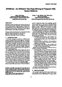
Figure 1: Our flash testing board The flash testing board can test two chips simultaneously and, combined with an FPGA board and a current meter, supports high-resolution timing and power measurements.
FLASH MEMORY
used to store bad block information, ECC, and other meta-data. NAND flash devices support three primary operations: erase, program, and read. Erase operates on entire blocks and sets all the bits in the block to 1. Program operations write entire pages at once and can only change 1s to 0s, so an erase operation (of the entire block) is required to arbitrarily modify the page’s contents. Read operations read an entire page in parallel. Table 1 reports the typical and maximum latencies and power usage for each of these operations. The time and power to transfer data across the pins and into or out of the internal buffer, for program and read operations respectively, are not included in these numbers. In addition to these primary commands, flash devices also support a variety of other operations, such as copyback-read and copyback-program [2]. These commands increase performance by avoiding unnecessary operations or by skipping bus transfers between the controller and the chip. Performance and power Currently, most flash devices transmit and receive data and commands over an 8- or 16-bit bus and can send and receive a new data word every 25-30ns (33-40Mhz). In theory, this interface could provide 33-80MB/s of bandwidth, but read and program latencies limit performance in practice. Unfortunately, the speed of this interface has not increased since 1995. Industrial efforts [1] are underway to remedy these problems and promise to raise peak bus bandwidth to between 133 and 400MB/s. Read, program, and erase operations all require different amounts of power. Datasheets give a maximum current draw of between 20mA and 30mA at 2.7-3.3V for a peak power of 50100mW. Reliability Flash memories can fail in a wide variety of ways. Most notoriously, the devices wear out with use. After many repetitions, the erase and program process can cause cells to become unreliable due to charge trapping in the gate oxide. The expected lifetime of one block in a flash device is 10,000 program/erase cycles for MLC and 100,000 for SLC. Furthermore, some devices retain data for only one year when programmed at this lifetime. Flash devices report erase and program failures, and manufactures recommend that the entire block be removed from service if any data within that block experience an error that cannot be corrected with ECC. To maximize the lifetime of a flash chip, flash systems use wear-leveling [9, 11, 18] to ensure that blocks are erased with equal frequency. Bits can also become corrupt while stored in flash memory due to “read disturb” and “program disturb”. Neither phenomenon causes permanent cell damage. Program disturb causes corruption
Flash memory has risen to prominence over the last decade due to the growing popularity of mobile devices with large storage requirements (iPods, digital cameras, etc.). Currently, 64Gb flash devices are available [7] with larger sizes on the way. Despite continued density scaling, the basic performance (read, program, and erase latencies) of flash devices has been roughly constant for over a decade. Density scaling may begin to wane as well, since flash faces significant challenges in further scaling [4]. In recent years, the architecture community has started to investigate flash’s role in systems for a range of applications. These include hard disk caches [12, 5], solid-state disks [6], transactionalized SSD [13], mobile sensor networks [10], and data-centric computing [8]. Our goal is to provide additional insights in flash’s behavior to enable further research in these and other directions.
2.1
Flash memory overview
Flash memory is a complex technology, and many factors impact its overall performance, reliability, and suitability for a particular application. Below we give a brief description of flash technology and terminology. Then, we describe the aspects of flash memory behavior that we quantify in this paper. These include the performance and power consumption of individual operations, and a range of recoverable and unrecoverable failure modes to which it is susceptible. In this section, the facts and figures we provide for flash devices are typical values taken from publicly available data sheets. Values for specific devices are in Table 2 and Section 3. Flash technology Flash memories store data as charge trapped on a floating gate between the control gate and the channel of a CMOS transistor. Each gate can store one or more bits of information depending on whether it is a single-level cell (SLC) or a multi-level cell (MLC). Commercially available devices store between 1 and 4 bits per cell [16, 17, 7]. Modern SLC and MLC flash devices achieve densities of 1 bit per 4F 2 and 1 bit per 1F 2 (for 4 bit-per-cell MLC devices) where F is the process feature size (currently 34nm [15]), allowing for very high-density flash arrays. Internally, a flash chip is broken into one or more planes or banks. Depending on the device, planes are largely independent of one another, contain local buffering for read and program data, and perform some operations in parallel. Each plane, in turn, contains a set of blocks, each made up of 64 (SLC) or 128 (MLC) pages. Each page contains between 2112 and 8448 bytes. This includes a 2-8KB primary data area as well as an “out of band” data area
25
Abbrev. A-SLC2 A-SLC4 A-SLC8 B-SLC2 B-SLC4 E-SLC8 B-MLC8 B-MLC32 C-MLC64 D-MLC32 E-MLC8
Manufacturer A A A B B E B B C D E
Chips Measured 3 3 3 3 3 3 3 3 3 3 3
Cell Type SLC SLC SLC SLC SLC SLC MLC MLC MLC MLC MLC
Cap. (GBit) 2 4 8 2 4 8 8 32 64 32 8
Tech. Node (nm)
50 72 72 50
OOB (Bytes) 64 64 64 64 64 64 64 128 256 128 128
Page Size (B) 2048 2048 2048 2048 2048 2048 2048 4096 8192 4096 4096
Pgs/ Blk 64 64 64 64 64 64 128 128 128 128 128
Blk/ Plane 1024 4096 4096 2048 2048 4096 4096 2048 4096 4096 1024
Planes/ Die 2 1 2 1 2 1 1 2 1 1 1
Dies 1 1 1 1 1 2 1 2 2 2 2
Peak Bandwidth (MB/s)
475.6
138.2
344.0
Read Program Erase
100
150.1
because program operations on one page subject all the pages in the block to weak programming voltages. The effect is greatest for the pages immediately adjacent to the cells being programmed. To mitigate program disturb, flash manufacturers require (MLC) or strongly suggest (SLC) that pages within a block be programmed in order. This ensures that once a bit is written, it will only be subjected to one strong program disturbance. Read disturb occurs because the voltages used to read data from a flash cell also have a weak programming effect on the other pages in the same block. As a result, data near pages that are frequently read can be degraded by millions of reads. To correct these and the other types of errors, flash systems must use ECC.
281.2
Table 2: Parameters for the flash devices used in this study We characterized eleven devices from five manufactures.
80 60 40 20
3.1
E−MLC8
D−MLC32
C−MLC64
B−MLC8
B−MLC32
E−SLC8
B−SLC4
Figure 2: Peak device bandwidth The peak bandwidth that each device can deliver during single-plane operation.
Data collection hardware
ing them from commercially available flash-based USB “thumb drives” otherwise. We also built a simple protocol analyzer to reverse engineer the command sets for each flash device, since the command sets vary slightly between manufacturers. We have elected not to reveal the manufacturers of our devices. We are not interested in calling on manufactures to account for the performance of their products. Rather, our goal is to understand the range of flash behavior so that we (and other researchers) can better understand flash memory’s strengths and weaknesses.
Figure 1 shows a photo of our flash characterization board. The custom-built daughter board attaches to a Xilinx XUP board. The daughter board holds two flash chip test sockets with independent power planes and facilities for measuring the current that each chip consumes. The FPGA on the XUP board implements a custom flash controller that provides support for timing measurements with 10ns resolution. The FPGA also hosts a full-blown Linux distribution. A user space application drives the flash test board and collects the results. For power measurements we use a high-resolution current probe (Agilent 1147A) attached to an mixed-signal oscilloscope. The probe can measure current changes at up to 50Mhz, and the triggering capabilities of the scope allow us to capture data for individual flash operations.
3.2
B−SLC2
To directly measure flash chip characteristics, we built a customized flash testing rig that gives us direct control of the devices’ pins and provides facilities for measuring power consumption and operation latency. This section describes that hardware, the flash devices we used, and the data we collected.
A−SLC8
A−SLC2
CHARACTERIZING FLASH MEMORY
A−SLC4
0
3.
3.3
Basic operation performance
We began by measuring the latency of the basic flash memory operations. Figure 3 shows the latencies for reads (a), programs (b), and erases (c). For each operation we measured the latency on 16 blocks on each of two chips for each chip model. The read latency varies little by manufacturer or chip (except for C-MLC64), and are in good agreement with values from publicly available datasheets. MLC chips have, on average, longer and enormously variable program latencies, which we discuss in more detail below. Erase latency exhibits a smaller gap, but manufacturer B enjoys an advantage for SLC and E for MLC. The first anomaly in our data is the variation in program time within each MLC block. All of the MLC devices we tested exhibited a regular and predictable variation in program latency between pages within a block. For instance, for B-MLC32 the first four pages and every other pair of pages in each block are 5.8 times faster on average than the other pages. The performance for these pages matches the “typical” values from the data sheet, but
Flash devices
Table 2 summarizes the flash devices we characterize in this study. They come from five manufacturers and cover a range of capacities at technology nodes including (among others) 50nm and 72nm. Flash manufactures are guarded about the details of their devices (many do not publicly release the data sheets for their devices) and some flash devices themselves can be difficult to obtain in the small quantities we needed. We overcame these problems by purchasing flash chips from distributors when possible and remov-
26
4000
1800
3600
1600
3200
1600
(a)
E−MLC8
D−MLC32
B−MLC32
C−MLC64
E−SLC8
A−SLC2
E−MLC8
D−MLC32
B−MLC32
C−MLC64
E−SLC8
0 B−MLC8
400
0 B−SLC4
800
B−MLC8
1200
200 B−SLC2
E−MLC8
D−MLC32
B−MLC32
C−MLC64
E−SLC8
B−MLC8
B−SLC4
B−SLC2
A−SLC8
A−SLC4
A−SLC2
0
2000
400
A−SLC8
20
600
A−SLC4
40
800
A−SLC2
60
2400
B−SLC4
1000
2800
B−SLC2
1200
80
A−SLC8
1400
100
A−SLC4
Erase Latency (us)
120
2000 Program Latency (us)
Read Latency (us)
140
(c)
(b)
Figure 3: Flash operation latencies Average flash operation latency for reads (a), programs (b), and erases (c) over ten program/erase cycles for 16 blocks on each chip. Error bars represent one standard deviation. 2000
the other pages take well over a millisecond to program. For CMLC64 every other page is fast. Figure 4 summarizes the results and shows that the fast MLC programs are nearly as fast as SLC programs, while the slow pages are very slow indeed. This effect is well-known to flash designers, and arises from the assignment of bits within one MLC cell to separate pages. MLC cells can be in one of four states, depending on how much charge is present on the floating gate, which allows each cell to store two bits. To program either bit, the chip applies a programming pulse, reads the value, applies another pulse, and so on until the cell reaches the desired state. Since the high-order bits have a larger target range, the pulses can be relatively powerful and only a few are required. For the low-order bit the pulses are weaker and the program requires more of them, resulting in longer latencies. Section 4 demonstrates how exploiting this difference can significantly improve flash drive responsiveness and efficiency. SLC chips show no corresponding variability. The second surprise in our investigation is that performance varies predictably as the devices begin to wear out. Figure 5 shows average program latency as a function of erase count for our SLC chips. The data show that program performance increases as the device wears out, resulting in nearly 50% faster program operations over the lifetime of an SLC device. MLC devices show much less variation: their performance increases by only 10-15%. This effect is due to charge trapping or breakdown of the gate oxide. As the oxide becomes a less effective insulator, it easier to move charge across it onto the gate. The same phenomenon is responsible for the eventual failure of the cell, since it also makes it easier for charge to leak off the floating gating. We discuss a potential application of this phenomenon in Section 4. Figure 2 summarizes the bandwidth that each device can deliver during single-plane operation. This value is a function of the operation latency, the page size, and the bus cycle time. For our experiments we used a 30ns cycle time for sending and receiving data to and from the chip. With a 20ns cycle time (the next faster clock available on our testing rig), none of the chips operated properly, although some are rated to 25ns. The motivation for MLC manufacturers to increase page size is clear: programming more bits in parallel allows them to nearly match SLC’s programming bandwidth, despite their greater program latency.
3.4
Fast 50% Slow 50%
Program Latency (us)
1800 1600 1400 1200 1000 800 600 400 200
E−MLC8
D−MLC32
C−MLC64
B−MLC32
B−MLC8
E−SLC8
B−SLC4
B−SLC2
A−SLC8
A−SLC4
A−SLC2
0
Figure 4: The programing speed anomaly Average programming speed for over ten program/erase cycles for 16 blocks on each chip. Programming speed varies dramatically between pages in MLC devices in a predictable pattern. SLC chips show no such variation. Error bars represent one standard deviation. average power for our chips by using a high-speed amp-meter to measure the current draw while the chips performed various operations. Table 3 summarizes the results. The table presents peak power, average power, idle power, and per-operation energy for each operation. The average power is measured for a sequence of operations running as quickly as our test setup can drive the chip. We calculate peak power by dividing the energy for a single operation (measured using our amp meter) by its latency. The table breaks out MLC energy by “fast” and “slow” pages and shows a disparity similar to the one we observed for program time. The pages that are fastest to program also consume dramatically less energy per operation (because program power is constant). Again, SLC chips show no page-to-page variation. The table also shows that SLC enjoys a large efficiency advantage over MLC for all three operations as well as idle power. The exception is E-MLC8, whose remarkably small erase latency provides an correspondingly small erase energy. Excluding the erase energy of E-MLC8, MLC consumes 2.05, 2.70, and 1.13 times more energy per bit for read, program, and erase operations, respectively. They also consume 1.83 times more idle power, on average.
Basic operation power consumption
A key advantage of flash memory over spinning disks is its low power consumption. Unfortunately, datasheet power numbers do not lead to good power modeling. We measured both peak and
27
Peak Read Power in mW (transfer) Peak Erase Power in mW Peak Program Power in mW (transfer) Ave Read Power (mW) Ave Erase Power (mW) Ave Program Power (mW) Idle Power (mW) Read Energy (nJ/bit) Program Energy (nJ/bit) Erase Energy (nJ/bit) Peak Read Power in mW (transfer) Peak Erase Power in mW Peak Program Power in mW (transfer) Ave Read Power (mW) Ave Erase Power (mW) Ave Program Power (mW) Idle Power (mW) Read Energy (nJ/bit) Fast Program Energy (nJ/bit) Slow Program Energy (nJ/bit) Erase Energy (nJ/bit)
A-SLC2 35.3 (19.2) 30.9 55.2 (43.2) 10.3 27.2 27.9 2.7 0.052 0.72 0.06 B-MLC8 54.0 (29.1) 42.4 58.9 (22.4) 18.1 45.5 46.5 12.7 0.15 1.09 3.31 0.070
A-SLC4 41.1 (18.3) 35.5 59.9 (39.2) 14.0 38.4 32.4 7.1 0.069 0.61 0.067 B-MLC32 75.9 (41.1) 70.6 94.7 (63.1) 31.1 53.0 52.5 8.5 0.11 0.96 3.30 0.056
A-SLC8 58.8 (33.1) 47.6 78.4 (59.9) 21.0 44.4 50.1 17.0 0.088 0.97 0.093 C-MLC64 112.0 (42.8) 111.8 132.2 (65.2) 41.5 105.0 77.0 27.3 0.19 0.66 2.86 0.038
B-SLC2 27.2 (9.3) 25.3 35.0 (13.6) 7.4 27.6 19.6 2.9 0.046 0.47 0.011 D-MLC32 66.3 (31.2) 57.0 82.3 (31.7) 28.3 56.2 55.6 11.2 0.093 0.79 2.84 0.051
B-SLC4 29.9 (8.2) 20.0 35.0 (8.4) 11.0 22.9 20.8 2.9 0.042 0.41 0.025 E-MLC8 13.4 (39.9) 21.3 118.4 (28.5) 21.3 23.5 40.9 10.2 0.002 0.46 2.07 0.0057
E-SLC8 19.1 (60.8) 25.5 56.0 (33.5) 18.8 20.8 37.5 13.3 0.0056 1.01 0.031
Table 3: Power and energy consumption for flash operations Peak values are taken from measuring consumption during a single operation with our high-resolution amp meter. The power measurements for operations and the associated data transfer are listed separately. Average values are taken over multiple operations on our test system. 400
Reliability Program Latency (us)
3.5
One of the most oft-cited concerns about flash memory is its reliability. Flash memories can corrupt data in three main ways. The most important mechanism, wear-out, causes physical damage to the cells and is not reversible. The two remaining mechanisms, program disturb and read disturb, do not cause physical damage and are fully reversible. Manufacturers recommend that systems use error correction codes and access pattern restrictions to recover from or prevent all three types of errors. The datasheets for flash chips provide a rating telling how many erase cycles a block can undergo before it is no longer reliable. For SLC chips this is typically 100,000 cycles, and for MLC it is typically 10,000. Our results show that these ratings tell only part of the story. To measure the effect of wear on reliability, we stress-tested flash chips by performing 10 erase-program-read cycles in which we wrote random data to each page, and then read the data to chack for errors. Then, we performed 990 erase-program operations, also with random data. We repeated this process until we had reached 1 million erases for SLC chips and 100,000 erases for MLC chips. Figures 6 and 7 show the error rate for each chip. The difference between SLC and MLC is stark. MLC devices show significant error rates from the very beginning. For most of the MLC models, the error rate increases sharply shortly after their rated lifetime, and some start to increase sharply even earlier. SLC devices, by contrast, show almost zero errors until they reach their rated lifetime and maintain reasonably low rates for up to six times their rated lifetime. Wear out also has an adverse effect on data “shelf life.” Although we have not quantified this effect, flash designers tell us that for recent flash devices the data shelf life can be as low as one year for the blocks that are close to their rated lifetime. Regardless, our data show that for such applications with less stringent shelf life requirements, the maximum number of erase/program cycles before SLC chips become unusable may be much higher.
A-SLC2 A-SLC4 A-SLC8 B-SLC2 B-SLC4 E-SLC8
350 300 250 200 150 100 50 0 0
50000
100000
150000
200000
Program/Erase cycles
Figure 5: Program performance over time For SLC devices, average program time drops by nearly 50% over the 100,000 program/erase cycles of the chip. MLC devices (not shown) show a much smaller, 10-15% decline. The data also show a marked difference in reliability among pages in MLC devices. Figure 9 plots the total error rate for four chips over their rated lifetime of 10,000 program/erase cycles. Interestingly, although roughly half the pages in a block are significantly more reliable than the others, and there seems to be a pattern within the block, there is not a consistent correlation between program speed and reliability. SLC devices show similar variation, but error rates do not become significant until long past their rated lifetime. Program disturb To quantify program disturb, we erased a block and repeatedly programmed half of one page to 0. After each program we measured the number of unintentionally programmed bits in the block. Figure 8 shows how the bit error rate increases with the number of reprograms. For SLC devices, we observed no program disturb for the first 100 iterations. At this point, several of the chips developed dis-
28
8e-05
Bit error rate
6e-05 5e-05 4e-05 3e-05
3e-07 1.4e-06 1.2e-06 1e-06 8e-07 6e-07 4e-07 2e-07 0
B-MLC32-1 B-MLC32-2 D-MLC32-1 D-MLC32-2 C-MLC64-1 C-MLC64-2 B-MLC8-1 B-MLC8-2 E-MLC8-1 E-MLC8-2
0
2000
A-SLC2 A-SLC4 2.5e-07 A-SLC8 B-SLC2 2e-07 B-SLC4 E-SLC8
Bit error rate
7e-05
4000
1.5e-07 1e-07
2e-05
5e-08
1e-05 0 0
3000
6000
9000
12000
0
15000
0
Program/Erase cycles
200000
300000
Program/Erase cycles
Figure 6: Wear out and error rate for MLC devices The error rate for MLC devices increases dramatically with wear, and is non-zero even for brand-new devices (inset). There is also large variation in the change in error rate between instances of the same chip (notably D-MLC32-1 and D-MLC32-2).
Figure 7: Wearout and error rate for SLC devices For SLC devices, the error rates are several orders of magnitude lower than for MLC even at three times their rated lifetimes. Only A-SLC4 shows a significant increase. 0.02
tinctive patterns of errors. B-SLC4, A-SLC2 and A-SLC4 had increasing errors on every other page with no errors on the reprogrammed page or the two adjacent pages. E-SLC8 developed errors only in the first few pages. B-SLC2 and A-SLC8 developed no clear pattern. Figure 10 shows a representative sample of these patterns. For MLC devices, the results were more immediate. For all of the MLC chips, performing just one repeat program of certain pages revealed two distinct patterns of errors. For C-MLC64, reprogramming pages 2n would disturb nearly all the bits in page 2n − 3, except for the first two pages (which caused no errors on other pages) and the last two pages (which caused errors on pages 123 and 125). Additionally, 32 bit errors occur on the reprogrammed block itself. For the other chips, reprogramming pages 4n or 4n + 1 disturbs nearly all the bits in pages 4n − 6 and 4n − 5 except for the first four pages (which cause no errors) and the last four pages (which cause errors on pages 118, 119, 122 and 123). Read disturb To measure the prevalence of read disturb, we wrote a test pattern to several blocks on the flash chip and then repeatedly read the pattern back, checking to see if any errors had appeared. Figure 11 graphs the results. Our data show that, in most cases, the effects of read disturb began to appear between 250 thousand and 4.8 million repeated reads.
4.
100000
E-SLC8 B-MLC32 C-MLC64 D-MLC32 E-MLC8
0.018 0.016 Bit error rate
0.014 0.012 0.01 0.008 0.006 0.004 0.002 0 0
200
400
600
800
1000
Number of Reprograms
Figure 8: Program Disturb Most MLC devices experience a sharp increase in error rates near a certain number of reprograms.
4.1
A variation-aware FTL
The data in Section 3 demonstrated two sources of variation in program time. The first was the wide variation in program speed and energy consumption between the “fast” and “slow” pages in MLC devices. The second was the change in SLC program latency as the chips aged. We have developed a flash translation layer (FTL) called Mango to exploit the first variation to improve performance and/or power efficiency. We used the FTL described in [6] as the baseline FTL. The FTL provides a disk-like, block-based interface while distributing erase and program operations evenly across the flash memory to ensure uniform wear-out. The FTL maintains a map between logical block addresses (LBAs) and physical flash addresses (PFAs). The FTL maintains a “write point” at which all program operations occur. With each new write request, the FTL writes the new data at the current write point and updates the map so that the LBA in the write request points to the data that were just written. It then advances the write point. When the write point reaches the end of a block, the FTL must locate a new, erased block for a new write point. It keeps a pool of
APPLICATIONS
The ultimate goal of this work is to understand the performance of flash memories so that we can identify new ways to exploit their performance and overcome their limitations. The following sections demonstrate how we can apply the understanding that Section 3 provides to accomplish this. We explore two applications. The first is a new flash translation layer (FTL) that takes advantage of the fast/slow page phenomenon to increase responsiveness and decrease power consumption. The second is the application of a different data encoding scheme to increase flash’s effective lifetime. These applications demonstrate that understanding flash’s characteristics in detail can lead to significant system-level improvements.
29
Error Rate
B-MLC8
DMLC32-1
4e-07
4e-07
3e-07
3e-07
2e-07
2e-07
1e-07
1e-07
0
0 0
20
40
60
80
100
120
0
20
40
Error Rate
C-MLC64
60
80
100
120
80
100
120
D-MLC32-2
4e-07
4e-07
3e-07
3e-07
2e-07
2e-07
1e-07
1e-07
0
0 0
20
40
60
80
100
120
0
20
40
Page # within a block
60
Page # within a block
Figure 9: Per-page error rates for MLC devices MLC chips show large variation in error rates among pages in a single block. The y-axis measures the total raw error rate over the chips’ rated lifetime. The two chips at right are supposedly identical parts, but show very different error rates.
Error Rate
B-SLC4
A-SLC2
0.5
0.2
0.4
0.16
0.3
0.12
0.2
0.08
0.1
0.04
0
0 0
10
20
30
40
50
60
0
10
20
Error Rate
E-SLC8
30
40
50
60
40
50
60
B-SLC2
0.6 0.5 0.4 0.3 0.2 0.1 0
0.6 0.5 0.4 0.3 0.2 0.1 0 0
10
20
30
40
50
60
0
10
Page # within a block
20
30
Page # within a block
Figure 10: Program Disturb for SLC devices after 10,000 reprograms of page 32 Varied error patterns emerge when a page is repeatedly reprogrammed. The reprogrammed page consistently shows no errors.
Error Rate
E-MLC8
E-SLC8
0.00012 0.0001 8e-05 6e-05 4e-05 2e-05 0
0.00012 0.0001 8e-05 6e-05 4e-05 2e-05 0 0
2e+06
4e+06
6e+06
8e+06
1e+07
0
2e+06
A-SLC8
6e+06
8e+06
1e+07
8e+06
1e+07
A-SLC4
5e-06 Error Rate
4e+06
4e-05 3.5e-05 3e-05 2.5e-05 2e-05 1.5e-05 1e-05 5e-06 0
4e-06 3e-06 2e-06 1e-06 0 0
2e+06
4e+06
6e+06
8e+06
1e+07
Number of Reads
0
2e+06
4e+06
6e+06
Number of Reads
Figure 11: Read disturb up to 10 Million re-reads Repeatedly reading a page without refreshing the data causes a steadily increasing number of errors beginning at between 250 thousand and 4.8 million reads.
30
"�� "�� "�� "�� ��! ��� ��� ��� ���
2.0
2.0
Baseline Mango
1.8
1.8
1.6 1.4 1.2 1.0 0.8 0.6
1.4 1.2 1.0 0.8 0.6
0.4
0.4
0.2
0.2
0.0
0.0 Build DeskDevFinancial Average
����� �� ��� � � ���� �������
Baseline Mango
1.6 Normalized Wear
���������� #�������
������#��$� #���#��$�
"�!
Normalized Energy Consumption
������������� �� ������
���
Build DeskDevFinancial Average
"��������� ������&������ "����"����� ������&�"�����
"�! "�� "�� "�� "�� ��! ��� ��� ��� ���
���
����������� ��& �������� ��& ������������� ����������
"�! "�� "�� "�� "�� ��! ���
2.0 1.8 1.4 1.2 1.0 0.8 0.6
���
0.4
���
0.2
���
0.0 �!��� ��� �"��������� �"�����
� ��� ������! �������� �!�����
Baseline Mango
1.6 Normalized Wear
�������%����������������
���
�������%��� ����&�����!�� ���
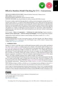
Figure 12: Mango results for the swap scenario Mango is able to significantly increase responsiveness for swap requests while only marginally increasing energy consumption and increasing wear by only 3%.
Build DeskDevFinancial Average
Figure 13: Mango results for the Netbook scenario Mango is able to significantly reduce the energy drain on the battery without significantly increasing energy while plugged in. It also realizes a slight performance increase, while increasing wear by 55%.
Name
Description
Build Financial [3] DesktopDev
Compile Linux kernel Live OLTP trace 24 hour software development desktop trace Virtual memory for desktop applications
SwapSpace
Mean Req. KB Read Write 3.7 4.0 2.3 3.7 17.0 4.0
7.8
4.0
% Reads 12.14 15.40 65.81
84.07
Table 4: Workloads for evaluating Mango The traces cover a wide range of application types.
two write points (using techniques described in [8]), one in an old, fast block and one in a young, slow block. We present results here for the MLC case. There are several dangers in this scheme. The first is increased wear for MLC devices because skipping half of the pages in each block means that we will need to erase blocks more frequently. The second danger is that ignoring pages will increase the frequency of garbage collection and ultimately increase latency for disk-bound applications. Finally, there is a limitation on how many pages we can skip. Skipped pages appear as invalid pages, and at any time there must be enough valid pages to account for the full, advertised capacity of the SSD. The result is that in some cases, the FTL can be forced to use slow pages during garbage collection. We evaluate our new FTL in two different scenarios: • Swap This scenario uses high-priority accesses for write requests for paging out virtual memory pages. We interleaved requests from the SwapSpace (see Table 4) trace with requests from other traces so that swap requests accounted for between 5 and 20% of the total requests. We measure the average latency for swap and non-swap requests separately. Garbage collection occurs in “slow” mode, unless it is required to service a high-priority request.
erased blocks for this purpose. If the pool falls below a “low water mark,” the FTL will perform a garbage collection in which it finds a block with some invalid data (i.e., data for which a newer version exists elsewhere in the array), completes the current operation and continues cleaning in the background. The FTL repeats this process until the pool reaches a “medium water mark.” When the number of empty blocks reaches the “high water mark,” the FTL stops background cleaning to avoid unnecessary erases. Mango exploits the variation in program time between the fast and slow pages by skipping slow pages for improved performance or power/energy efficiency for some operations. Mango adds a priority to incoming IO requests. For highpriority writes, the FTL will do its best to use fast pages. The FTL also provides a fast garbage collection mode that uses fast pages for garbage collecting write operations as well. Since the fast pages are also lower energy, high priority accesses are also low energy. To find a fast page, Mango uses the next fast page at the current write point for MLC devices. For SLC devices, it could maintain
• Netbook This scenario models a mobile device in which energy saving is key. When the device is running from its battery, all operations are tagged as high priority and the FTL is always in fast mode. When the device is running off of wall power, all operations are low priority and garbage collection occurs in slow mode. To model this scenario, we switch from battery to wall power at irregular intervals so that half of the trace is processed in each mode.
31
5
Normal WOM
2.5
Lifetime Improvement
2 1.5 1 0.5 0
Normal WOM
4 3 2 1
Figure 14: Effective program energy Because WOM codes decrease the number of erases per logical bit programmed, using them reduces programming energy by 9.5% on average.
Logical bits 00 01 10 11
First generation 111 110 101 011
E−MLC8
D−MLC32
C−MLC64
B−MLC8
E−MLC8
D−MLC32
B−MLC32
C−MLC64
E−SLC8
B−MLC8
B−SLC4
B−SLC2
A−SLC8
A−SLC4
A−SLC2
0 B−MLC32
Write Energy (nJ/logical bit)
3
Figure 15: Effective device lifetime Measured in logical bytes written before the device reaches the fatal error rate, WOM codes allows up to 5.2 times longer lifetime. Figure 13 shows the results for the netbook scenario. Here, we are most concerned about overall energy consumption, and Mango reduces energy consumption compared to the baseline by 3% on average while increasing wear by 55%. This increase is larger than for the swap scenario because a larger fraction of accesses were high priority.
Second generation 000 001 010 100
4.2
Flash-aware data encoding
Flash devices require the use of error correction codes to detect and recover from errors caused by wear, program-disturb, and read-disturb effects. Their performance, as well as their lifetime, can also be improved by using alternative data encoding schemes. The data in Section 3 provide us with the means to evaluate the impact of different encoding schemes on flash longevity. To demonstrate this, we have implemented and evaluated the performance of a simple write-once-memory (WOM) coding scheme for flash memory [14]. WOM codes were originally developed for storage devices punch cards and early digital optical disks, for example - in which a stored ’1’ could not be changed to a ’0’. This property would nominally prevent the user from writing more than once to any given bit of the storage medium. WOM codes provided a method to overcome this limitation, allowing a trade-off between the number of writes and the recorded data density (the number of logical bits stored in a physical bit location on the medium). Table 5 illustrates a simple WOM code that we have implemented. It uses three physical bits to represent two logical bits and allows two logical sets of bits to be written. Each sequence of two bits has two representations, one for the first program and one for the second. These are the first and second generation code words. The key to the code is that, with one exception, the 1s in each second generation code word are a superset of the 1s in all of the first generation code words. As a result, overwriting a first generation word with a second generation word always results in the second generation code word being stored. The exception is that the first and second generation code words are complements, so that the second generation pattern cannot be programmed. This leads to ambiguity in decoding, which the code resolves by reading the data before programming it and only reprogramming logical bits that have changed. In the context of flash memory, this encoding scheme allows us to write data to a block twice before erasing it. The data in
Table 5: The write-only memory code Write-only memory codes (WOM codes) allow multiple logical value to be written even if physical bits can only transition once. In each scenario we use a set of traces summarized in Table 4. The traces are from several sources and represent a wide range of application behaviors. The traces include operation arrival times, and we use that to schedule arrival times at the SSD. We implemented Mango in a flash memory simulator using the performance and power measurements from Section 3.3 to determine the latency for each operation (including garbage collection time if the operation needed to wait for it) and the overall energy consumption for the trace. The simulator collects statistics on the distribution of high and low priority accesses due to external IO requests and internal garbage collection operations. It also measures the fraction of slow pages that the FTL skipped during the trace and the total number of erases performed to gauge the amount of wear caused by the trace. The simulator models an SSD comprised of a single flash chip. For this study we used the data for chip C-MLC64 from Section 3, since the power and performance for the other MLC devices were comparable, we would expect similar performance and energy results. Figure 12 summarizes the results for the swap scenario and compares the responsiveness and power consumption of Mango with the baseline FTL. The data show that Mango achieves its goal of reducing swap latency: On average swap write requests complete 1.5 times more quickly with Mango than with the baseline. As we expected, the downside of increasing priority on some requests is increased overall wear. In this case, wear increased by an average of 3% across the traces.
32
REFERENCES
Section 3 showed that, for MLC devices, program disturb is only a problem for programing half of the pages in a block. Those pages are unsuitable for WOM codes. The other pages, however, can accept multiple programs with no ill effects. We refer to these pages as “WOM safe.” For SLC devices, program disturb is not a problem for the first few iterations on any page, therefore all page are WOM safe. The writing procedure is as follows. Initially, we program unencoded data into the non-WOM safe pages and first-generation WOM-encoded data into the WOM-safe pages. On the second programming pass, we program second-generation WOM-encoded data into just the WOM-safe pages. WOM-enconding is 66% efficient, so the two writes to the WOM-safe pages combined with a single write to unsafe pages gives a 1.16 times increase in the number of bytes that can be written to a block per erase operation for MLC. For SLC, there is a factor of 1.33 increase. This leads to two favorable trade-offs. First, WOM codes allow the chip to expend less energy to program a given amount of data. This is because the energy to erase is not required as frequently with respect to writes. Figure 14 displays these energy savings for each chip. The second measurable advantage of using WOM codes is a commensurate increase in useful device lifetime. We measure this as the amount of logical data written to the device before begins to experience the fatal error rate. This is the error rate at the recommended lifetime of the device under normal operation (without reprogramming or WOM-encoding). Figure 15 shows this increase in effective lifetime. SLC chips are not graphed because the WOM-encoded chips showed no errors even after programming 1.33 times more data than the baseline. We would expect a 17% (MLC) or 33% (SLC) increase in the number of bytes programmed for every erase, but several of the chips far exceed this expectation. There are several possible explanations. For example, reprogramming bits to the same value may reinforce the data or the WOM codes may have some other error-reducing properties. These are questions we are still exploring.
5.
[1] Onfi: Open nand flash interface. http://onfi.org/specifications. [2] Onfi: Open nand flash interface specification 2.0. http://onfi.org/wpcontent/uploads/2009/02/onfi_2_0_gold.pdf. [3] Umass trace repository. http://traces.cs.umass.edu/index.php/Storage/Storage. [4] International technology roadmap for semiconductors: Emerging research devices, 2007. [5] M. Baker, S. Asami, E. Deprit, J. Ouseterhout, and M. Seltzer. Non-volatile memory for fast, reliable file systems. In ASPLOS-V: Proceedings of the fifth international conference on Architectural support for programming languages and operating systems, pages 10–22, New York, NY, USA, 1992. ACM. [6] A. Birrell, M. Isard, C. Thacker, and T. Wobber. A design for high-performance flash disks. Technical Report MSR-TR-2005-176, Microsoft Research, December 2005. [7] e. a. C. Trinh. A 5.6mb/s 64gb 4b/cell nand flash memory in 43nm cmos. In Solid-State Circuits Conference. IEEE, 2009. [8] A. M. Caulfield, L. M. Grupp, and S. Swanson. Gordon: using flash memory to build fast, power-efficient clusters for data-intensive applications. SIGPLAN Not., 44(3):217–228, 2009. [9] L.-P. Chang. On efficient wear leveling for large-scale flash-memory storage systems. In SAC ’07: Proceedings of the 2007 ACM symposium on Applied computing, pages 1126–1130, New York, NY, USA, 2007. ACM. [10] P. Juang, H. Oki, Y. Wang, M. Martonosi, L. S. Peh, and D. Rubenstein. Energy-efficient computing for wildlife tracking: design tradeoffs and early experiences with zebranet. In ASPLOS-X: Proceedings of the 10th international conference on Architectural support for programming languages and operating systems, pages 96–107, New York, NY, USA, 2002. ACM. [11] D. Jung, Y.-H. Chae, H. Jo, J.-S. Kim, and J. Lee. A group-based wear-leveling algorithm for large-capacity flash memory storage systems. In CASES ’07: Proceedings of the 2007 international conference on Compilers, architecture, and synthesis for embedded systems, pages 160–164, New York, NY, USA, 2007. ACM. [12] T. Kgil, D. Roberts, and T. Mudge. Improving nand flash based disk caches. In ISCA ’08: Proceedings of the 35th International Symposium on Computer Architecture, pages 327–338, Washington, DC, USA, 2008. IEEE Computer Society. [13] V. Prabhakaran, T. L. Rodeheffer, and L. Zhou. Transactional flash. USENIX Symposium on Operating Systems Design and Implementation, 2008. [14] R. Rivest and A. Shamir. How to reuse a write-once memory. Information and control, 55:1–19, December 1982. [15] e. a. R.W. Zeng. A 172mm2 32gb mlc nand flash memory in 34nm cmos. In Solid-State Circuits Conference. IEEE, 2009. [16] e. a. S. Chang. A 48nm 32gb 8-level nand flash memory with 5.5mb/s program throughput. In Solid-State Circuits Conference. IEEE, 2009. [17] e. a. T. Futatsuyama. A 113mm2 32gb 3b/cell nand flash memory. In Solid-State Circuits Conference. IEEE, 2009. [18] D. Woodhouse. Jffs2: The journalling flash file system, version 2. http://sources.redhat.com/jffs2/.
CONCLUSION
The devices we characterized in this study exhibited variation both within a block and over time in terms of power consumption, latency, and error rates. Our data also show that the values manufacturers provide in publicly available datasheets often tell only part of the story, and that actual performance can be significantly worse and highly variable. Our application case studies demonstrate that by looking beyond the datasheets manufacturers provide, we can make significant improvements to flash-based storage devices. Exploiting two of the effects we measured enabled us to significantly decrease latency for critical IO requests and extend the effective lifetimes of chips.
ACKNOWLEDGEMENTS This work was funded by NSF Awards 0643880 and 0811794 and with support from the Center for Magnetic Recording Research at the University of California, San Diego.
33