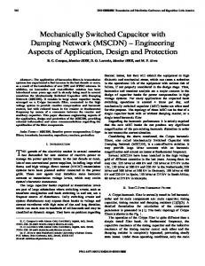
Class E Resonant Rectifier with a Series Capacitor. Marian K. Kazimierczuk, Senior Member, IEEE, Bogdan Tomescu, Member, ZEEE, and Alexandru IvaScu.
IEEE TRANSACTIONS ON CIRCUITS AND SYSTEMS-I
FUNDAMENTAL THEORY AND APPLICATIONS,VOL. 41, NO. 12, DECEMBER 1994
885
Class E Resonant Rectifier with a Series Capacitor Marian K. Kazimierczuk, Senior Member, IEEE, Bogdan Tomescu, Member, ZEEE, and Alexandru IvaScu
circuit is sinusoidal input voltage U . Consequently, the current through the capacitor C and the inductor L is a portion of a sinusoid. This current shapes the voltage across the capacitor and the inductor in accordance with the equation ic = C d v c / d t and V L = L d i L / d t , respectively. At wot = 0, the derivative of the inductor voltage d v L / d t is zero because the derivative of the inductor current is constant at turn-off. Then the inductor voltage V L gradually decreases, crosses zero, becomes negative, reaches its peak value, and increases to VO.The diode voltage waveform V D is similar to the inductor voltage VL, but is shifted downwards by a dc voltage VO. I. INTRODUCTION When the diode voltage reaches its threshold voltage (0.7 V LASS E inverters can be successfully used together with for a silicon pn junction diode), the diode turns on. It can be Class E rectifiers [1]-[9] in resonant dc-dc converters, seen that the diode turns off and on at low d v D / d t , reducing yielding higher density high-power supplies. Basically, there switching losses and noise. are two groups of Class E rectifiers: low d v l d t and low dildt When the diode is ON, the inductor is shunted by the output rectifiers. The primary advantage of these circuits are soft dc voltage VO;hence, the inductor current Z L rises linearly. switching, low switching losses, and low noise levels. The aim The capacitor voltage wc is a fraction of the sinusoidal input of this paper is to present an analysis of a new Class E resonant voltage shifted downwards by a dc voltage Vo. Therefore, the low dwldt rectifier, design equations, and experimental results. capacitor current is a portion of a cosinusoid with a step change The rectifier can be used in resonant dc-to-dc converters. at turn-on as nothing limits the derivative of the capacitor current d i c l d t . The diode current io, being the difference between the capacitor current and the inductor current, has the 11. CIRCUUDESCRIPTION A circuit of the new Class E resonant voltage-driven low same step change at turn-on. Its average value equals the load d w l d t rectifier with a series capacitor is shown in Fig. l(a). current IO.Once the diode current io reaches zero, the turnIt consists of a resonant capacitor C , a resonant inductor off transition of the diode begins. In the case of the pn junction L, a diode, and a first-order low pass output filter C ~ - R L .diode, the reverse recovery should be considered. In the Class Resistor RL represents a dc load. The rectifier is driven E rectifier, the reverse-recovery current is low because d i D / d t by a sinusoidal voltage source U . The ac source v and the before turn-off is low. During the storage time, this current is rectifier can be coupled by an isolation transformer to provide a portion of a sine wave and the voltage is about 0.7 V. After the desired ac-to-dc voltage transfer. Although the leakage the storage time, the diode current decreases to zero and the inductance and the diode capacitance are not incorporated into diode voltage is held low by the V L - VOvoltage, reducing the the rectifier topology, the circuit has good performance at high turn-off power loss due to the reverse recovery. In the Class E frequencies. A dc-to-dc converter can be obtained by replacing rectifier, the diode ON duty cycle D can be in the range from the sinusoidal input voltage v by a dc-to-ac inverter with a zero to 1. The diode current contains a relatively low amount parallel-resonant circuit. Fig. 1(b) and (c) depicts equivalent of harmonics, reducing the EMI/RFI level.
Abstract-An analysis and experimental results are given for a Class E resonant low dvldt rectifier with a series resonant capacitor. The circuit contains two resonant components: a capacitor and an inductor. It is driven by a sinusoidal voltage source whose amplitudemust be controlled to obtain a constant-voltageoutput. The rectifier exhibits a peculiar behavior because its equivalent input reactance changes discontinuously from inductive to capacitive when the load varies from infinity to zero. Design equations are derived using Fourier series techniques. The theory is compared with experimental results obtained for the rectifier operating at 1 MHz ac input and 5 V dc output.
C
circuits of the rectifier for the intervals when the diode is OFF and ON, respectively. The principle of operation of the rectifier is explained by current and voltage waveforms, which are shown in Fig. l(d). When the diode is OFF, the capacitor C and the inductor L form a series-resonant circuit. The voltage across the resonant Manuscript received August 6, 1993; revised March 4, 1994. This work was supported by the National Science Foundation under Grant ECS-8922695. This paper was recommended by Associate Editor David Haigh. M. K. Kazimierczuk is with the Department of Electrical Engineering, Wright State University, Dayton, OH 45435 USA. B. Tomescu is with Space SystemsLoral, Palo Alto, CA 94303 USA. A. Ivqcu is with Electronics Research Institute, 72321 Bucharest 30, Romania. B E E Log Number 9406541.
nI.
ANALYSIS
A. Assumptions The analysis of the rectifier begins with the following assumptions: 1) The diode is ideal. 2) The filter capacitance C f is large enough that the ripple on the dc output voltage is very small and, therefore, the C ~ - R circuit L can be replaced by a dc voltage sink. 3) The rectifier is driven by an ideal sinusoidal voltage source.
1057-7122/94$04.00 0 1994 IEEE
886
IEEE TRANSACTIONS ON CIRCUITS AND SYSTEMS-I: FUNDAMENTAL THEORY AND APPLICATIONS, VOL. 41, NO. 12, DECEMBER 1994
2
0
6
4
8
10
Q (b)
Fig. 2. Voltage transfer function M versus diode ON duty ratio D and normalized load resistance Q. (a) M as a function of D . (b) M as a function of Q.
B. Characteristics of the Rectijier The subsequent analysis uses the following definitions: the angular resonant frequency
1
WO
=-
m
the characteristic impedance of the resonant circuit
-
the normalized load resistance
the ac-to-dc voltage transfer function
-Y--7
md
(4 Fig. 1. Class E zero-voltage-switching low d v l d t rectifier. (a) Circuit. (b) Model of the rectifier when the diode is OFF.(c) Model of the rectifier when the diode is ON. (d) Waveforms.
4) The operating frequency f is equal to the resonant frequency fo = 1 / ( 2 ~ m ) .
M=
2. Vm
(4)
The input voltage is sinusoidal in accordance with assumption 3) and is given by
w = Vmsin(w0t + 4).
(5)
The waveforms of the diode current io and the diode voltage W D normalized with respect to the dc output current
KAZIMIERCZUK et ~ l . CLASS : E RESONANT RECTIFIER WITH A SERIES CAPACITOR
IO and the dc output voltage VO are, respectively, iD IO
$[cos(wot
("
+ 4 ) - cos 4
-M(wot - 27r)],
1
for 0
< wot 5 2 4 1 - 0 )
for 27r(l- D) < wot
5 27r (6)
+
cos(w0t 4 ) -cos+sinwot] +coswot - 1, for 0 < wot 5 % ( I - 0 ) for 2 4 1 - 0 ) < wot 5 27r. (7) -[wot
k
These waveforms are shown in Fig. l(d). The initial phase 4 and the diode duty cycle D are related by (8), shown at the bottom of this page. As D increases from 0 to 1, 4 increases from 0 to 180". The ac-to-ac voltage transfer function is given in (9), also shown at the bottom of this page. Plots of M versus D and Q are depicted in Fig. 2. The transfer function M decreases from 00 to zero as D is increased from zero to 1. This occurs when Q is decreased from 00 to zero. Note that M is almost a linear function of Q. The relationship among Q , D , M , and 4 is
.2
0
.6
.4
(a)
Y
\
e 3
\
e. 0
6
4
(l-cos27rD)sin+ 27r
+ (T - D)cos4 + 7rD2M. (10)
As Q is increased from zero to 00,D decreases from 1 to zero. Since the input voltage is sinusoidal, the power content of higher harmonics is zero. Therefore, it is sufficient to consider the rectifier's input impedance 2; for the fundamental. This impedance can be represented as a parallel combination of an input resistance R; and an input reactance X ; . The input resistance Ri at the fundamental frequency f normalized with respect to the load resistance RL is
Hence, one obtains the input resistance R; normalized with respect to 20 = w0L
(b)
Fig. 3. R, / RL and R, / W O L (or W O CR,) as functions of the diode ON duty cycle D and the normalized load resistance Q. (a) R, / RL and R, / W O L (or woCR,) versus D. (b) R , / R L and R,/woL (or woCR,) versus Q.
to capacitive as load varies. This change is discontinuous. The input reactance is inductive, given by Xi = w0Li for Q > 2.066 (in which case, D < 0.325) and capacitive, given by X ; = -l/(woCi) for Q 5 2.066 (in which case, D 2 0.325). Thus, for the two intervals of D (or Q), one obtains (13) and (14) found at the bottom of the next page. Ratios of L ; / L and Ci/C as functions of Q and D are shown in Fig. 4(a) and (b), respectively. The peak value of the diode current IDMoccurs at the end of the OFF interval wot = 27r(l - 0 ) for D < 0.34 (i.e., M > 1) and at the maximum of the waveform given by (6) for D 2 0.34 (i.e., M 5 1). The peak diode current is 2~
IDM Fig. 3 shows plots of &/RL and Ri/Zo as functions of D and Q. The input reactance X i changes from inductive
tan4 =
M=
I11
10
8
Q
M =
1
D
+
2 '1,
[ 7 r + ~ sin ?rDsin 7rD-q5
$[cos(arcsinM ) +M(arcsin M
-
for0 < D
cos 4
+ 4)1,
for 0.34
5 0.34
< D 5 1. (15)
+
cos2 27rD 2 4 1 - 2 0 ) sin 27rD - 4[1+ 7 r 2 D ( 1- D)] cos 27rD 3 [l - cos27rD 47r2D(1 - D)]sin27rD - 2 ~ ( 1 D)(1 - cos27rD) '
+
. r r ( l - ~ ) s i n 2 7 r ~ s i n 4 [++ s i n 2 ~ ~ + 7 r- (Dl) C O S ~ ~ ~ D ] C O S + 1 - COS 2nD
(9)
IEEE TRANSACTIONS ON CIRCUITS AND SYSTEMS-I:
FUNDAMENTAL THEORY AND APPLICATIONS, VOL. 41, NO. 12, DECEMBER 1994
4
-
0
2
4
6
8
.2
Q
.6
.8
1
D
(4 lo
.2
.4
10
(a)
0
IDM/I~
_____...__...... ...
2
.6
.4
.8
4 L
1
D (b) Fig. 4. L , / L (or C,/C) versus the diode ON duty ratio. D and the normalized load resistance Q. (a) L , / L (or C,/C) versus Q. (b) L , / L (or C , / C ) versus D.
Fig. 5. Normalized peak values of diode current I D M / Z O and diodereverse voltage VDMIVO as functions of D and &. (a) z D M / z O and VDM/VOVerSUs D.(b) z D M / z O and V D M / V O versus Q.
Ratio IDM/IO is plotted versus D and Q in Fig. 5(a) and (b), normalized output-power capability is respectively. It can be seen that I D M / I Oincreases from 2 to 00 as Q increases from zero to 00, or as D decreases from 1 to zero, respectively. The peak value of the diode reverse voltage VDMcan be The maximum value of cp occurs at D = 0.5 and equals found by differentiating the diode voltage waveform in (7) 0.0999. Various parameters of the rectifier are given in Table I. and setting the result to zero. Only numerical results can be obtained. VDM/VOagainst D and Q is shown in Fig. 5(a) IV. DESIGNEXAMPLE and (b), respectively. As D increases from zero to 1, or as Q decreases from 00 to zero, VDM/VOincreases from 2 to Design a transformerless version of the Class E rectifier CO. Note that the absolute value of I D Mdecreases with Q at a of Fig. l(a) to meet the following specifications: Vo = 5 V, fixed value of Vi.On one hand, IO = VO/RLdecreases while I o = 0 to 0.1 A, and f = 1 MHz. RL increases. On the other hand, I D M / I Oincreases while RL The dc load resistance RL varies from its minimum value increases. However, the rate of increase of I D M / I Ois smaller R L = V0/Iom, ~ ~ ~= 5/0.1 = 50 R to 00. The dc output than the rate of decrease of IO.Therefore, the maximum values power varies from its maximum value PO = VOIOmiLX= of IDM occurs at the minimum load resistance R L ~The ~ ~5 .x 0.1 = 0.5 W to zero. Assume D = 0.5 at full load
,
I,
889
KAZIMIERCZUK er al.: CLASS E RESONANT RECTIFIER WITH A SERIES CAPACITOR
33
y I r -Il '----
v0=5v
- - - bneasured
f = l MH?
-
Calculated
iD
20
0
t
0
E
>
10
C 1
50 100 200 500 lk 2k
20
5k
'.
m
RL(Q) Fig. 6 . Measured and calculated plots of the amplitude V, of the input voltage as a function of the load resistance RL at f = 1 MHz. TABLE I PARAMETERS OF CLASSE RECTIFIER
iD
~ ~
~
Q
D
M
Q
R.JwaL,w.CR,
RJRL
IDMJIO VDRMJVO L S L , C S C
~
0 10 0.20 0.25 0.30 0.35 0.40 0 45 0.50 0.55 0 60 0.65 0.70 0.75 0.80 0.90
23.9793 15.8860 31.4243 47.5835 3.7761 7.2214 59.0029 2.2772 42424 70.0365 14485 26117 80.6156 0.9448 1.6379 90.7019 0.6207 1.0283 100.2842 0.4055 06385 109 3723 0 2605 0.3884 117.9889 0.1629 0.2293 126.1638 0.0979 0.1301 133 9301 00557 0.0699 0.0349 141.3220 0.0294 148.3743 0.0139 00158 155 1234 OW56 0.0061 167 8770 00003 0.0004
0.0020 0.0623 0.0351 0.2532 0.0964 0.4091 0.6224 0 2383 0.9174 0.5601 1.3343 1.2976 1.9416 3 0407 2.8613 7.3669 183536 4.3234 6.7915 52.2192 11.2822 161.3710 20.2764 580.2204 40.7502 2584 6138 96.5825 15813.4550 I 476.2380 4174485 25
19.6171 8.6233 6.0265 4.1170 4 6159 3.6355 3 1047 2 7777 2.5599 2.4062 2 2928 2.2065 2.1397 2.0881 2.0219
2.0911 2.3125 2 4550 2.6184 2.go68 3.0266 3.2872 3.6012 3.9873 4.4726 5.0999 5 9399 7.1198 8.8936 17.7783
0.2083 0.7378 1.5602 6.3202 0.1854 0.4359 0.6193 0.7521 0.8460 0.9100 0.9514 0.9764
0 0 VD
0.9901
0.9966 0.9999
istance R L , ~ =~ 50 R because the power-output capability es on the maximum value at D = 0.5. Hence, from Table L = R ~ , i ~ / ( 0 . 3 8 8 4 ~ 0=) 50/(0.3884 x 2 7 ~x lo6) = 5pH. From (l), C = l/(Lw;) = 1/20.5 x x (2 x 7r < lo6)' = 1.236 nF. From Table I, the amplitude of the input voltage can be found as V, = V o / M = 5/0.2605 = 19.19 V. the maximum values of the diode current and voltage occur at all full load resistance R L ~Using ~ ~Table . I, I , I D M = 2.77710,~~= 2.777 x 0.1 = 277.7 mA and VDM= 3.601Vo = 3.601 x 5 = 18 V.
re ta I, 2(
iD
0 0 VD
V. EXPERIMENTAL RESULTS
The circuit of the Class E rectifier of Fig. I(a) designed in the proceeding section was built using R L = 50 R, C = 1.2 nF, L = 20.5 pH, C j = 2 x 470 nF (two ceramic capacitors in parallel) and an 11DQ03 Schottky diode. The circuit was driven by a power sinusoidal generator at f = 1 MHz. A dc output of Vo = 5 V was obtained at V, = 19.2 V. Fig. 6 shows measured and calculated plots of the input voltage V, as a function of the load resistance RL at Vo = 5 V and f = 1 MHz. The amplitude V, decreased with increasing load RL. The discrepancy between the calculated and measured plots can be attributed to parasitic components, especially the diode offset voltage. Fig. 7 shows experimental waveforms of the diode current i~ and the diode voltage V D at Vo = 5 V and f = 1 MHz for R L = 50,100 and 500s1.
(C)
Fig. 7. Experimental waveforms of the diode current io and thediode voltage un. (a) RL = 50 11 (full power). (b) RI, = 100 R ( 50% of full power). (c) RL = 500 0 (10% of full power). Vertical: 0.2 A and 10 V/div.; horizontal: 200 ns/div.
Fig. 8 shows waveforms of the capacitor current ic and the , with the diode voltage I I D , for full inductor current i ~ together power. The efficiency of the rectifier was 91% at 10 = 0.1 A. VI. CONCLUSION A new Class E resonant low dvldt rectifier was analyzed, design equations were derived, and experimental results were
890
IEEE TRANSACTIONS ON CIRCUITS AND SYSTEMS-I:
FUNDAMENTAL THEORY AND APPLICATIONS, VOL. 41, NO. 12, DECEMBER 1994
[7] M. K. Kazimierczuk and K. Puczko, ‘‘Class E low d v / d t synchronous rectifier with controlled duty ratio and output voltage,” IEEE Trans. Circuits Syst., vol. 38, pp. 1165-1 172, Oct. 1991. [XI A. Ivascu, M. K. Kazimierczuk, and S . Birca-Galateanu, “Class E resonant low d u / d t rectifier,” IEEE Trans. Circuits Syst., vol. vol. 39, pp. 604-613, Aug. 1992. [9] -, “Class E resonant low d ? / d t rectifier,” IEE Proc. P a n G, Circuits, Devices and Syst., vol. 140, Dec. 1993, pp. 417423.
(b) Fig. 8. Experimental waveforms of the resonant capacitor current i ~ .and the inductor current i ~ along , with the diode voltage 77~3 at R L = 50 C l (full power). (a) Waveforms of 7, and P D . (b) Waveforms of i L and P D . Vertical: 0.2 A and IO V/div.; horizontal: 200 ns/div.
given. Although the transformer leakage inductance and the diode capacitance are not incorporated into the rectifier circuit, the rectifier proves to have good performance at high frequencies. The diode ON duty cycle can take any value between zero and 1 and is independent of the filter capacitance. Since the diode turns on at low dvldt and turns off at zero d w l d t , switching losses, noise, and the reverse recovery effect are low. The rectifier acts like an impedance inverter for the entire range of D from zero to 1 and therefore one can connect this circuit as a load of a Class E amplifier.
Marian K. Kazimierczuk (M’91-SM’91) received the M.S., Ph.D., and D.Sci. degrees in electronics engineenng from the Department of Electronics, Technical University of Warsaw, Warsaw, Poland, in 1971, and 1978, and 1984, respectively. He was a teaching and research assistant from 1972 to 1978 and Assistant Professor from 1978 to 1984 with the Department of Electronics, Institute of Radio Electronics, Technical University of Warsaw, Poland. In 1984, he was a project engineer for Design Automation, Inc., Lexington, MA. In 1984 and 1985, he was a Visiting Professor with the Department of Electrical Engineering, Virginia Polytechnic Institute and State University, VA. Since 1985, he has been with the Department of Electrical Engineering, Wright State University, Dayton, OH, where he is currently a Professor. His research interests are in resonant and PWM dc/dc power converters, dc/ac inverters, high-frequency rectifiers, electronic ballast, magnetics, power semiconductor devices, and high-frequency high-efficiency power tuned amplifiers and lighting systems. He has published more than 130 technical papers, more than 60 of which have appeared in IEEE Transactions and Journals. Dr. Kazimierczuk received the IEEE Harrell V Noble Award in 1991 for his contributions to the fields of aerospace, industnal, and power electronics He is also a recipient of the 1991 Presidential Award for Faculty Excellence in Research and the 1993 Teaching Award from Wright State University. ON CRCUITS AND He serves as an Associate Editor of IEEE TRANSACTIONS SYSTEMS and as an Associate Editor for the Journal of Circuits, Systems and Computers.
Bogdan Tomescu (M’91) was born in Bucharest, Romania, in 1963. He received the MSEE degree from the Politechnic Institute of Bucharest in 1987. Shortly afterward he joined the Bucharest Electrotechnics Research Institute, and in 1990 he was appointed to the Chair of Applied Electronics at the Electronics Engineenng Department of the Politechnic Institute of Bucharest as an Assistant Professor Since 1993 he is with Space SystemsLoral, Palo Alto, CA. His research interests include power electronics and control systems, particularly SMPS, modeling and simulation of dc-dc topologies and analog and digital circuit design.
REFERENCES [ I ] M. K. Kazimierczuk and J. Jbiwik, “Class E resonant rectifiers,” in Proc. 31st Midwest Symp. Circuits and Sysr., St. Louis, MO, August 10-12, 1988, pp. 138-141. [2] -, “Class E zero-voltage-switching rectifier with a series capacitor,” IEEE Trans. Circuits Syst., vol. 36, pp. 926-298, June 1989. [3] M. K. Kazimierczuk, ‘‘Class E low d i , n / d t rectifiers,” Proc. Inst. Eng., Pr. B, Electric Power Appl., vol. 136, Nov. 1989, pp. 257-262 [4] M. K. Kazimierczuk and J. Jbiwik, “Class E zero-voltage-switching and zero-current-switching rectifiers,” IEEE Trans. Circuits Syst., vol. 37, pp. 4 3 W 4 4 , Mar. 1990. [5] M. K. Kazimierczuk, “Analysis of Class E zero-voltage-switching rectifier,” IEEE Trans. Circuits Syst., vol. 37, pp. 747-755, June 1990. [6] M. K. Kazimierczuk and J. Jbiwik, “Analysis and design of Class E zero-current switching rectifier,” IEEE Trans. Circuits Syst., vol. 37, pp. 1000-1009, Aug. 1990.
Alexandru IvaScu received the M.S. and Ph.D. degrees in electronics and communications engineering from the Department of Applied Electronics, Polytechnic Institute of Bucharest, Bucharest, Romania, in 1971 and 1990, respectively. Since 1971, he has been with Electronic Research Institute, Research and Development Department for Professional Communications Equipment, Bucharest, Romania, where he is involved in designing and development of prototypes of communications equipment. His research interests are in VHF communications equipment, high-frequency amplifiers, PWM dc/dc power converters, and high-frequency rectifiers.